三星移动硬盘M3中文版使用手册(2)CHS_Samsung Drive Manager User's Manual Ver 2.7 (1)
三星 SCH-E339 用户指南说明书

8
从主屏幕启动或取消静音
模式 ( 按住 )
/cn
中国印刷 GH68-38046A 中文 12/2012. 版本 1.0
电池充电
安装存储卡
设备接受最大容量为 32 GB 的存储卡。 根据存储卡的生 产商和类型,有些存储卡可能与您的设备不兼容。
连接到电源插座
1. 将充电器较小的一端插入设备的多功能插孔,较大的 一端插入标准电源插座。
如欲在信息中附加文件,按下 <选项> → 添加多媒体 并选择文件。 5. 按下 发送。
查看信息
按下收件箱并选择要阅读的信息。
管理联系人
将姓名,电话号码和个人信息等数据保存在设备内 存,UIM 卡中。
<功能表> → 电话本
要更改存储位置,请按 <功能表> → 电话本 → <选项> → 设定 → 存储新联系人到并选择存储 位置。
然后再次按下 [ ] 拨打号码。 • 要使用通讯录拨打电话,请按 <功能表> → 电话本,
选择联系人并按 [ ]。 • 如欲接听来电,按下 [ ]。
发送和查看信息
<功能表> → 信息
发送信息
1. 按下写信息。 2. 按下添加打开通讯录。 3. 选择联系人,然后按下添加。
或者输入联系人的号码。 4. 向下滚动并输入文本消息。 请参阅“输入文本”。
访问功能表
如欲访问设备的功能表或选项,
按导航按钮 确认按钮 <功能表> <返回>
[]
滚动到各个功能表。 启动一个功能表或应用程序。 打开功能表屏幕。 返回上一个屏幕。 关闭功能表或应用程序,然后返回主 屏幕。
• 当访问需要输入 PIN2 码的功能表时,必须输 入随 UIM 卡提供的 PIN2 码。 有关详细信息, 请联系服务提供商。
三星 CK3 手持计算机 accessories 说明书
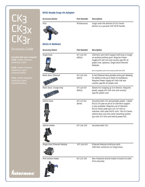
850-819-001 (AA23)
Snap-on Vocollect audio adapter for wired head set support
Not compatible with CK3X / CK3R
Batteries & Chargers
Accessory Name Standard Capacity Battery Pack
318-034-003 One (1) standard rechargeable 18.5
ห้องสมุดไป่ตู้
(AB18)
watt hours (5100 mAh) battery pack
CK3X ships with (1)
Extended Capacity ‘Smart’ Battery Pack 318-046-011 (1001AB01)
850-823-001 (1007AA01)
CK3 Snap-on audio adapter. Provides quick disconnect audio jack for use with wired headset.
Not compatible with CK3X / CK3R
850-817-001 (AA23)
Docks & Modules
Accessory Name Single Dock
Multi-Dock, Ethernet Multi-Dock, Charge Only
Part Number
871-228-101 (AD20)
Description
USB Host and Client Support with bay to charge an auxiliary battery pack. Requires Power Supply 851-061-502 and country specific AC power cord. Optional: Single Dock Ethernet Modules.
三星 SyncMaster 2033SN 2233SN LCD 显示器 说明书
SyncMaster 2033SN/2233SNLCD 显示器用户手册安全说明符号注请务必遵守这些安全说明,以确保人身安全和防止财产损失。
请务必仔细阅读这些说明,并以正确的方法使用本产品。
警告/注意否则可能导致人身伤亡。
否则可能导致人身伤害或财产损失。
标记惯例禁止很重要,任何时候都要阅读并了解。
请勿拆卸将电源插头从插座上拔下请勿触摸接地以防止触电电源长时间不使用显示器时,请将您的计算机设置为 DPM。
如果使用屏幕保护程序,请将其设置为活动画面模式。
此处提供的图片仅供参考,不适用于所有情况(或国家/地区)。
“消除残影”功能说明的快捷方式请勿使用破损的电源线或电源插头以及破损或松动的电源插座。
•否则可能导致触电或起火。
将电源插头拔出或插入电源插座时,请勿用湿手触碰电源插头。
•否则可能导致触电。
确保将电源线连接到接地的电源插座。
•否则可能导致触电或人身伤害。
确保电源插头牢固正确地插入电源插座。
•否则可能导致起火。
请勿强行弯折或拉扯电源插头,也不要将任何重物压在其上。
•否则可能导致起火。
请勿将多台设备连接到同一个电源插座。
•则可能因过热导致起火。
请勿在使用本产品时断开电源线连接。
•否则可能会由于触电而损坏本产品。
要断开设备的电源,必须将插头从电源插座拔出,因此电源插头应易于操作。
•否则可能引起火灾或触电。
仅可使用本公司提供的电源线。
请勿使用其他产品随附的电源线。
•否则可能导致起火或触电。
安装如果要在多尘、高温或低温、湿度高或含化学物质的环境安装显示器,以及在需要 24 小时不间断运行的机场或火车站等地方安装显示器,请务必与授权服务中心联系。
否则,显示器可能会严重损坏。
搬动显示器时小心不要使产品坠落。
•这可能会导致产品损坏或人身伤害。
请确保至少由两个人搬移本产品。
•否则可能将其跌落,而导致人身伤害甚或损坏本产品。
在将本产品安装到柜子中或架子上时,请确保本产品底部的前端没有突出来。
•否则,产品可能坠落或造成人身伤害。
三星 S3C84H5 F84H5 8-BIT COMOS 说明书

S3C84H5/F84H58-BIT COMOSRevision 1.00April 2010用户手册2010 Samsung Electronics Co., Ltd. All rights reserved.Important NoticeThe information in this publication has been carefully checked and is believed to be entirely accurate at the time of publication. Samsung assumes no responsibility, however, for possible errors or omissions, or for any consequences resulting from the use of the information contained herein.Samsung reserves the right to make changes in its products or product specifications with the intent to improve function or design at any time and without notice and is not required to update this documentation to reflect such changes.This publication does not convey to a purchaser of semiconductor devices described herein any license under the patent rights of Samsung or others. Samsung makes no warranty, representation, or guarantee regarding the suitability of its products for any particular purpose, nor does Samsung assume any liability arising out of the application or use of any product or circuit and specifically disclaims any and all liability, including without limitation any consequential or incidental damages. "Typical" parameters can and do vary in different applications. All operating parameters, including "Typicals" must be validated for each customer application by the customer's technical experts. Samsung products are not designed, intended, or authorized for use as components in systems intended for surgical implant into the body, for other applications intended to support or sustain life, or for any other application in which the failure of the Samsung product could create a situation where personal injury or death may occur.Should the Buyer purchase or use a Samsung product for any such unintended or unauthorized application, the Buyer shall indemnify and hold Samsung and its officers, employees, subsidiaries, affiliates, and distributors harmless against all claims, costs, damages, expenses, and reasonable attorney fees arising out of, either directly or indirectly, any claim of personal injury or death that may be associated with such unintended or unauthorized use, even if such claim alleges that Samsung was negligent regarding the design or manufacture of said product.S3C84H5/F84H5 8-BIT COMOS用户手册, Revision 1.00Copyright 2010 Samsung Electronics Co., Ltd.All rights reserved. No part of this publication may be reproduced, stored in a retrieval system, or transmitted in any form or by any means, electric or mechanical, by photocopying, recording, or otherwise, without the prior written consent of Samsung Electronics.Samsung Electronics Co., Ltd.San #24 Nongseo-Dong, Giheung-GuYongin-City, Gyeonggi-Do, Korea 446-711TEL : (82)-(31)-209-3865FAX : (82)-(31)-209-6494Home Page: Printed in the Republic of KoreaRevision History修订版本号修订日期修订内容作者第一版HM, CHENG1.00 2010年4月 -Table of Contents1产品概述.......................................................................................................1-11.1 S3C8-系列 MCU......................................................................................................................................1-11.2 S3C84H5/F84H5 MCU............................................................................................................................1-11.3 特性.........................................................................................................................................................1-21.3.1 CPU..................................................................................................................................................1-21.3.2 存储器..............................................................................................................................................1-21.3.3 时钟源..............................................................................................................................................1-21.3.4 指令集..............................................................................................................................................1-21.3.5 指令执行时间...................................................................................................................................1-21.3.6 中断..................................................................................................................................................1-21.3.7 I/O Ports............................................................................................................................................1-21.3.8 Timer/Counters.................................................................................................................................1-21.3.9 Watch Timer.....................................................................................................................................1-21.3.10 A/D转换器.......................................................................................................................................1-31.3.11 异步 UART....................................................................................................................................1-31.3.12 PWM 模块......................................................................................................................................1-31.3.13 SIO..................................................................................................................................................1-31.3.14 内置RESET电路(LVR)...................................................................................................................1-31.3.15 震荡频率.........................................................................................................................................1-31.3.16 工作温度范围.................................................................................................................................1-31.3.17 工作电压范围.................................................................................................................................1-31.3.18 现有封装形式.................................................................................................................................1-31.4 内部模块框图...........................................................................................................................................1-41.5 管脚分布图..............................................................................................................................................1-51.6 管脚分布图..............................................................................................................................................1-51.7 管脚分布图..............................................................................................................................................1-61.8 管脚特性描述...........................................................................................................................................1-71.9 管脚电路................................................................................................................................................1-10 2地址空间.......................................................................................................2-12.1 概述.........................................................................................................................................................2-12.2 程序存储空间(ROM)................................................................................................................................2-22.2.1 Smart Option.....................................................................................................................................2-32.3 寄存器结构..............................................................................................................................................2-42.3.1 寄存器页面指针(PP).........................................................................................................................2-62.3.2 寄存器SET 1....................................................................................................................................2-72.3.3 寄存器SET 2....................................................................................................................................2-72.3.4 主寄存器空间...................................................................................................................................2-82.3.5 工作寄存器.......................................................................................................................................2-92.3.6 使用寄存器指针..............................................................................................................................2-102.4 寄存器寻址............................................................................................................................................2-122.4.1 通用工作寄存器区(C0H-CFH)........................................................................................................2-142.4.2 4 位工作寄存器寻址方式................................................................................................................2-152.4.3 8 位工作寄存器寻址方式................................................................................................................2-172.5 系统和用户栈.........................................................................................................................................2-192.5.1 栈操作............................................................................................................................................2-192.5.2 用户自定义栈.................................................................................................................................2-192.5.3 栈指针(SPL, SPH)..........................................................................................................................2-19 3寻址模式.......................................................................................................3-13.1 概述.........................................................................................................................................................3-13.1.1 寄存器寻址模式(R)...........................................................................................................................3-23.1.2 间接寄存器寻址模式(IR)..................................................................................................................3-33.1.2.1 间接寄存器寻址模式(续).........................................................................................................3-43.1.2.2 间接寄存器寻址模式(续).........................................................................................................3-53.1.2.3 间接寄存器寻址模式(续).........................................................................................................3-63.1.3 偏址寻址模式(X)...............................................................................................................................3-73.1.4 直接寻址模式(DA)..........................................................................................................................3-103.1.4.1 直接寻址模式(续)..................................................................................................................3-113.1.5 间接寻址模式(IA)............................................................................................................................3-123.1.6 相对地址寻址模式(RA)...................................................................................................................3-133.1.7 立即数寻址模式(IM).......................................................................................................................3-14 4控制寄存器...................................................................................................4-14.1 概述.........................................................................................................................................................4-14.2 Register Description.................................................................................................................................4-14.2.1 Register Map....................................................................................................................................4-14.2.1.1 ADCON - A/D 转换控制寄存器: F7H Set1, Bank0...............................................................4-54.2.1.2 BTCON - Basic Timer 控制寄存器 : D3H Set1......................................................................4-64.2.1.3 CLKCON - 系统时钟控制寄存器 : D4H Set 1........................................................................4-74.2.1.4 FLAGS - 系统标志寄存器: D5H Set 1...................................................................................4-84.2.1.5 IMR - 中断屏蔽寄存器: DDH Set 1.......................................................................................4-94.2.1.6 IPH - 指令指针(高字节) : DAH Set 1....................................................................................4-104.2.1.7 IPL - 指令指针(低字节) : DBH Set 1.....................................................................................4-104.2.1.8 IPR - 中断优先级寄存器: FFH Set 1, Bank 0......................................................................4-114.2.1.9 IRQ - 中断请求寄存器: DCH Set 1.....................................................................................4-124.2.1.10 OSCCON - 时钟控制寄存器 : F2H Set 1, Bank0............................................................4-134.2.1.11 P0CON - Port 0 控制寄存器(高字节) : E6H Set 1, Bank 0..............................................4-144.2.1.12 P1CONH - Port 0 控制寄存器(高字节) : E8H Set 1, Bank 0..............................................4-154.2.1.13 P1CONL - Port 1 控制寄存器(低字节) : E9H Set 1, Bank 0...............................................4-164.2.1.14 P1INTPND - Port 1 中断标志位寄存器: EAH Set 1, Bank0..............................................4-174.2.1.15 P1INT - Port 1 中断使能: EBH Set 1, Bank 0...................................................................4-184.2.1.16 P2CONH - Port 2 控制寄存器(高字节) : ECH Set 1, Bank0...............................................4-194.2.1.17 P2CONL - Port 2 控制寄存器(低字节) : EDH Set 1, Bank0...............................................4-204.2.1.18 P2PUR - Port 2 上拉电阻控制寄存器: FAH Set 1, Bank0................................................4-214.2.1.19 P3CONL - Port 3控制寄存器(低字节) : EFH Set 1, Bank0..................................................4-224.2.1.20 PP - 寄存器页指针: DFH Set 1.........................................................................................4-234.2.1.21 PWMCON - PWM 控制寄存器: F5H Set 1, Bank 1..........................................................4-244.2.1.22 RP0 - 寄存器指针0 : D6H Set 1........................................................................................4-254.2.1.23 RP1 - Register Pointer 1 : D7H Set 1.................................................................................4-254.2.1.24 SIOCON - SIO 控制寄存器: F2H Set 1, Bank1................................................................4-264.2.1.25 SIOPS - SIO 预分频寄存器: F0H Set 1, Bank1................................................................4-274.2.1.26 SPH - 堆栈指针(高字节) : D8H Set 1.................................................................................4-274.2.1.27 SPL - 堆栈指针(低字节) : D9H Set 1..................................................................................4-274.2.1.28 STPCON - STOP 控制寄存器: D1H Set 1,Bank0..........................................................4-284.2.1.29 SYM - System Mode Register : DEH Set 1.........................................................................4-284.2.1.30 T0CON - Timer 1(0) 控制寄存器: E8H Set 1, Bank 1.......................................................4-294.2.1.31 T1CON - Timer 1(1) 控制寄存器: E9H Set 1, Bank 1.......................................................4-304.2.1.32 TACON - Timer A 控制寄存器: E1H Set 1, Bank 1..........................................................4-314.2.1.33 TBCON - Timer B 控制寄存器: D0H Set 1.........................................................................4-324.2.1.34 TINTPND - Timer A, Timer 1中断标志位寄存器: E0H Set 1, Bank1.................................4-334.2.1.35 UARTCON - UART 控制寄存器: F6H Set 1, Bank 0........................................................4-344.2.1.36 UARTPND - UART 标志位和奇偶控制位: F4H Set 1, Bank 0............................................4-354.2.1.37 WTCON - Watch Timer 控制寄存器: F8H Set 1, Bank1...................................................4-36 5中断结构.......................................................................................................5-15.1 概述.........................................................................................................................................................5-15.1.1 中断级(Levels).................................................................................................................................5-15.1.2 中断向量(Vectors)............................................................................................................................5-15.1.3 中断源(Sources)...............................................................................................................................5-15.1.4 中断类型...........................................................................................................................................5-25.1.5 S3C84H5/F84H5中断结构................................................................................................................5-35.1.5.1 中断向量地址..........................................................................................................................5-45.1.5.2 使能/禁止中断的指令(EI, DI)..................................................................................................5-65.1.6 系统级中断控制寄存器.....................................................................................................................5-65.1.7 中断处理控制要点............................................................................................................................5-75.1.8 外围中断控制寄存器.........................................................................................................................5-85.1.9 系统模式控制寄存器(SYM)..............................................................................................................5-95.1.10 中断屏蔽寄存器(IMR)...................................................................................................................5-105.1.11 中断优先级控制寄存器(IPR)........................................................................................................5-115.1.12 中断请求寄存器(IRQ)...................................................................................................................5-135.1.13 中断标志位类型............................................................................................................................5-145.1.13.1 概述....................................................................................................................................5-145.1.13.2 硬件自动清零的标志位.......................................................................................................5-145.1.13.3 需在中断服务程序里手动清零的标志位..............................................................................5-145.1.14 中断响应的步骤............................................................................................................................5-155.1.15 中断服务程序...............................................................................................................................5-155.1.16 中断向量地址的生成....................................................................................................................5-165.1.17 中断嵌套.......................................................................................................................................5-16 6指令集..........................................................................................................6-16.1 概述.........................................................................................................................................................6-16.1.1 数据类型...........................................................................................................................................6-16.1.2 寄存器访问.......................................................................................................................................6-16.1.3 寻址模式...........................................................................................................................................6-16.2 标志寄存器(FLAGS)................................................................................................................................6-56.2.1 标志位描述.......................................................................................................................................6-66.2.1.1 C 进(借) 位标志(FLAGS.7)....................................................................................................6-66.2.1.2 Z 零标志位(FLAGS.6).............................................................................................................6-66.2.1.3 S 符号标志位(FLAGS.5).........................................................................................................6-66.2.1.4 V 溢出标志(FLAGS.4)............................................................................................................6-66.2.1.5 D 十进制调整标志(FLAGS.3).................................................................................................6-66.2.1.6 H 半字节进(借) 位标志(FLAGS.2).........................................................................................6-66.2.1.7 FIS 快速中断状态标志(FLAGS.1)...........................................................................................6-66.2.1.8 BA 寄存器块地址标志(FLAGS.0)...........................................................................................6-66.2.2 指令集符号.......................................................................................................................................6-7 6.3 条件码....................................................................................................................................................6-116.3.1 指令集描述.....................................................................................................................................6-126.3.1.1 ADC - 带进位加法(Add with Carry)......................................................................................6-136.3.1.2 ADD - 加法(Add)...................................................................................................................6-146.3.1.3 AND - 逻辑与(Logical AND).................................................................................................6-156.3.1.4 BAND - 位与(Bit AND)..........................................................................................................6-166.3.1.5 BCP - 位比较(Bit Compare).................................................................................................6-176.3.1.6 BITC - 位反(Bit Complement)...............................................................................................6-186.3.1.7 BITR - 位清零(Bit Reset)......................................................................................................6-196.3.1.8 BITS - 位置1(Bit Set)............................................................................................................6-206.3.1.9 BOR - 位或(Bit OR)..............................................................................................................6-216.3.1.10 BTJRF - 位测试,若为假相对跳转(Bit Test, Jump Relative on False)...............................6-226.3.1.11 BTJRT - 位测试,若为真,相对跳转(Bit Test, Jump Relative on True)............................6-236.3.1.12 BXOR - 位异或(Bit XOR)....................................................................................................6-246.3.1.13 CALL - 程序调用(Call Procedure)......................................................................................6-256.3.1.14 CCF - 进位标志位取反(Complement Carry Flag)...............................................................6-266.3.1.15 CLR - 清零(Clear)...............................................................................................................6-276.3.1.16 COM - 取反(Complement)..................................................................................................6-286.3.1.17 CP - 比较(Compare)...........................................................................................................6-296.3.1.18 CPIJE - 比较,增加一,若相等跳转(Compare, Increment, and Jump on Equal)..............6-306.3.1.19 CPIJNE - 比较,增加一,不等跳转(Compare, Increment, Jump on Non-Equal)..............6-316.3.1.20 DA - 十进制调整(Decimal Adjust).......................................................................................6-326.3.1.21 DEC - 字节减1(Decrement)................................................................................................6-346.3.1.22 DECW - 字减1(Decrement Word)......................................................................................6-356.3.1.23 DI - 屏蔽全局中断(Disable Interrupts)................................................................................6-366.3.1.24 DIV - 无符号除法(Unsigned Divide)...................................................................................6-376.3.1.25 DJNZ - 减1,如果非零,跳转(Decrement and Jump if Non-Zero)....................................6-386.3.1.26 EI - 使能全局中断(Enable Interrupts).................................................................................6-396.3.1.27 ENTER - 进入(Enter)..........................................................................................................6-406.3.1.28 EXIT - 退出(Exit).................................................................................................................6-416.3.1.29 IDLE - 空闲指令(Idle Operation).........................................................................................6-426.3.1.30 INC - 加1(Increment)..........................................................................................................6-436.3.1.31 INCW - 字加1(Increment Word).........................................................................................6-446.3.1.32 IRET - 中断返回(Interrupt Return)......................................................................................6-456.3.1.33 JP - 跳转(Jump)..................................................................................................................6-466.3.1.34 JR - 相对跳转指令(Jump Relative).....................................................................................6-476.3.1.35 LD - 传送数据(Load)...........................................................................................................6-486.3.1.36 LDB - 传送位数据(Load Bit)...............................................................................................6-506.3.1.37 LDC/LDE - 传送程序/外部数据存储器数据(Load Memory)................................................6-516.3.1.38 LDCD/LDED - 传送数据之后地址减1(Load Memory and Decrement)...............................6-536.3.1.39 LDCI/LDEI - 传送数据后地址加1(Load Memory and Increment).......................................6-546.3.1.40 LDCPD/LDEPD - 传送数据前地址减1(Load Memory with Pre-Decrement)......................6-556.3.1.41 LDCPI/LDEPI - 传送数据前地址加1(Load Memory with Pre-Increment)...........................6-56。
第三代极速柔性磁盘系列用户指南说明书

Handling PrecautionsAllow the drive to reach room temperature before installing it in the computer.Do not open the E S D bag until youÕre ready to install the drive. Handle the drive by its sides. Do not touch the circuit board (electronics). Do not connect/disconnect any drive cables while your computer is turned on.Do not drop, jar, or bump the drive.1PreIn s tallatio nT hank yo u fo r se le c ting a Maxto r hard d rive sto rag e p ro d uc t.Maxto r's g o al is to p ro vid e yo u w ith the m o st up -to -d ate p ro d uc t p o ssib le ,and w e are c o nstantly e nhanc ing o ur so ftw are and d o c um e ntatio n to b e tte r m e e t yo ur ne e d s .Ple ase visit o ur w e b -site at to vie w the late st that Maxto r has to o ffe r!System /OS Requirem ents¥ A full version of your operating system (OS) is required for a new hard drive installation(see kit package for details)Tools for InstallationThe following tools are needed to install your new M axtor hard drive:¥Small Phillips head screw driver ¥Small pair of pliers or tweezers ¥Your computer user manual ¥Operating system softwareBackup Your DataM axtor highly recommends that you make a backup copy of your files before installing the new M axtor hard drive.Please refer to your computer user manual for more information.2D r ive J um p e r S e t u p Configure the Drive J um persIf specific jumper options are needed for your system configuration, refer to the illustrations and definitions provided in this section.SCSI ID J umper SettingsM axtor SCSI drives typically ship from the factory with jumpers set to SCSI ID 6, and termination power jumped.SCSI ID 7 is usually reserved for the SCSI host adapter.3D rive InstallInstalling Drive Inside of Y our Com puter SystemM ake sure your com puter is pow ered dow n before installing the drive.The following illustrations are of typical computer systems and hard drive mounting styles.Your computer may have a different mounting style. Please refer to your computer user manual for more information.B e sure to secure the drive to the device bay with all four screws.The drive should be oriented with its printed circuit board facing down.Installing 5.25-inch Mounting BracketsIf the hard drive will be installed in a 5.25-inch device bay, attach mounting brackets (available separately) to the hard drive as shown in the figure below.Mounting ScrewsMounting ScrewsMounting BracketNote:M axtor LVD SCSI drives do not support on-board termination. M axtor recommends the use of Active LVD terminators and 68-pin twisted pair cabling.S CS I hos t adapter manufacturers us ually s upply proper cabling and termination with the purchase of an LVD S CS I hos t adapter.A ttention:The R ear J umper O ption Connector is an O E M specific con-nector. M ost installations will never use the jumper options on this connector. Always configure the drive using the jumpers at the Front J umper O ption Connector .Other J umper SettingsTP - Termination Pow er (12 Pin O ption Connector)Pins 11-12 T ermination power ensures that there is a sufficient power level along the entire SCSI bus. It is recommended that the final device on the SCSI bus have the Termination Power jumper installed. All devices in between the host and final device typically have no jumper on Termination Power.Note that Termination Power is not the same as on-board termination, which this drive does not support.S S - S tagger S pinPins 13-14 For most configurations this option is not utilized.M ost current SCSI host adapters offer a Start Unit command enable or disable, which supersedes the functionality of the SS jumper setting. W hen the Delay Spin (DS) jumper isenabled on the drive, the Start Unit command from the SCSI host adapter will send Start Unit commands to all devices on the bus at pre-determined intervals. This can help prevent power supply overload when running several devices on the SCSI bus.W P - W rite ProtectionPins 11-12 B y factory default, the drive is shipped with no jumper on these pins, and the drive can be written to unless protected by application software. W ith the pins jumped, the drive can be used as a read-only device. This feature prevents accidental overwrites and is useful for frequently accessed archives and reference files.Force S E Ð Force S ingle Ended O perationPins 17-18 By factory default, the drive is shipped with no jumper on these pins. W ith most system configurations, it is not necessary to use this jumper. LVD drives are multi-mode capable. They will automatically detect the presence of a sin-gle-ended bus and revert to single-ended mode.DS - Delay S pin Disable Delay S pin: No jumper across pins 15-16 (factory default). Disabling Delay Spin allows the drive to spin up when the system is powered up.Enable Delay S pin: J umper across pins 15-16 This setting will prevent the drive from spinning up until it receives a Start Unit command from a SCSI host adapter. M ost SCSI host adapters have the Start Unit command enabled by default in the host adapter BIOS. Enabling Delay Spin is only necessary when you are starting multiple devices at power on.S CS I IDPin numbers 1-8 are typically referred to in pairs as A0 (pins 1and 2), A1 (3,4), A2 (5,6), A3 (7,8). The jumper pairs will allow configuration of SCSI ID's 0 to 15. All SCSI devices must have an individual ID on the SCSI bus (there is no M aster/Slave set-ting). SCSI ID 7 is usually reserved for the SCSI host adapter.Fault LED and B usy O ut J umpersTypical installations do not require the use of the Fault LED and Busy Out jumpers. The Busy Out signal is usually supplied through the PCI bus to the PC motherboard's Busy indicator LED. If connecting the Busy Out jumper for a drive installed in an external case, please refer to the wiring documentation sup-plied by the manufacturer of the case. Connection of the Fault LED is not recommended in internal or external installations.Computer with available 3.5-inch device bayComputer with available 5.25-inch device bayD I e v i r D O t i B D I 1t i B D I 2t i B D t i B D I 0D I F F O F F O F F F O 1D I N O F F O F F F O 2D I F F O N O F F F O 3D I N O N O F F F O 4D I F F O F F O N F O 5D I N O F F O N F O 6D I F F O N O N F O 7D I T SO H I S C S R O F D E V R E S E R 8D I F F O F F O F F O N O 9D I N O F F O F F O N O 01D I F F O N O F F O N O 11D I N O N O F F O N O 21D I F F O F F O N O N O 31D I N O F F O N O N O 41D I F F O N O N O N O 51D I NO NO NO NO Pin 2Pin 1Pin 17Pin 18SCSI ID 3SCSI ID 2SCSI ID 1SCSI ID 0BUSY LED -/+WRT PROTECT STAGGER SPIN DELAY SPINSINGLE ENDEDFAULT LED GROUND GROUND BUSY LED GROUND TERM POWERSCSI ID 3SCSI ID 2SCSI ID 1SCSI ID 0NOT USED+5 VPin 1Pin 2Pin 11Pin 124 Pin PowerConnector12 Pin Option Connector68 Pin SCSIConnectorPin 168-pin Connector68-pin Drive ConnectorDC Power ConnectorUltra LVD/SE CablePower Supply Cable(3-Pin or 4-Pin)Bevel4Cable Hook-up Attach the SCSI and Power CablesIf the M axtor SCSI drive is the only device attached to the SCSI adapter card, attach the drive at the end of the Ultra LV D/SE cable, farthest from the SCSI adapter card. This connector has a beveled edge and will only fit one way. Then attach an external active LVD/SE SCSI terminator.Please refer to the SCSI adapter card user guide for additional recommendations on data cable place-ment and SCSI termination requirements.Attach a power cable to the power connector on the hard drive. This connector is keyed and willonly fit one way. Check all other cable connections before you turn on the computer.Caution:Do not force or rock the connectors into their sockets on the hard drive. Push them in straight until they are seated firmly.5P a r t it io n i n g F o r m a t t i n gMaxtor hard drives can accept nearly all operating systems. Some operating sys-tems have volume size limitations that may require you to partition your drive into multiple volumes. Please refer to your system or SCSI adapter card user guide for information about formatting and partitioning the drive.General Guidelines¥ DOS /W indow s 9X /M E:Use FDISK.EXE to partition and FORM to format the drive.¥ W indow s N T/2000:Boot your system from the installa-tion floppy disks provided with the OS to partition and format the drive.If you do not have the original installa-tion floppies, you can create them using your W indows installation CD.¥ W indow s X P:Boot your system from the W indows XP installation CD to partition and for-mat the drive. If your system is not capable of booting from a CD, you can download bootable W indows XP installation floppies from M icrosoft's website at ¥ Macintosh:Most non-Apple branded hard drives can be formatted using the Drive Setup utility included in Mac OS 8.6 and above. Mac OS versions before 8.6 will require a third-party hard drive utility such as FW B Hard Disk Toolkit () or Intech Hard Disk SpeedTools() to partition and initialize the drive. Please visit the FW B or Intech website for details on these non-Maxtor software products.www.maxtor.c om6P r o d u c t R e g i st r a t io nTake Advantage of the Benefits!By registering your new M axtor prod-uct,youll have the option to receive product updates, special offers, and other valuable information about other data storage solutions from M axtor.S imply point your web browser to:w w go to theproduct registration page, and com-plete the short questionnaire.Changes are periodically made to the information herein Ð which will be incorporated in revised editions of the publication. M axtor may make changes or improvements in the product(s) described in this publication at any time and without notice.Copyright © 2001 M axtor Corporation. All rights reserved. Printed in the U.S.A. 12/01. M axtor ¨is a regis-tered trademark of M axtor Corporation. Other brands or products are trademarks or registered trademarks of their respective holders.Active LVD TerminatorConnect to SCSI Host Adapter CardUltra LVD/SE CableStandard Cabling for Single SCSI Drive in System(Ultra LVD/ SE cable connections)Cable Connections for SCSI Drive。
三星移动硬盘M3中文版使用手册(2)CHS_Samsung Drive Manager User's Manual Ver 2.7 (1)

Samsung Drive Manager常见问题安装问题:我已连接 Samsung 外接硬盘,但系统没有任何反应。
回答:检查 USB 缆线连接。
如果已正确连接 Samsung 外接硬盘,其 LED 应会点亮。
回答:如果硬盘发出滴答声,表明电力不足。
如果当前USB 端口无法识别硬盘,请尝试将它连接到其他 USB 端口。
问题:我无法安装 Samsung Drive Manager。
回答:请检查使用Samsung 外接硬盘的最低系统要求。
有关更多信息,请参阅用户手册第 1 章中的“系统规格”。
问题:我在Windows Vista 上执行Samsung Drive Manager 时,“用户帐户控制”窗口始终显示。
如何才能让“用户帐户控制”窗口不显示?回答:需要提升权限才能使用Samsung Drive Manager 直接或间接访问外接硬盘。
如果未获得“用户帐户控制”访问权限,则会限制使用Samsung Drive Manager。
要让“用户帐户控制”窗口不显示,请选择“控制面板”上的“用户帐户”,然后设置“关闭用户帐户控制”。
Samsung AutoBackup问题:我应该备份哪些东西?回答:一般来说,应该备份使用其他软件生成的数据文件。
不建议备份程序文件,因为如果计算机出现问题,您必须重新安装这些程序。
建议您备份可以恢复的数据文件。
问题:我应该多长时间备份一次数据?回答:如果您没有定期备份,建议您备份重要的文件、个人数据(如照片)以及无法重新创建或难于创建的文件。
问题:某些文件已更改,但系统未执行实时备份。
回答:如果更改的文件未设置为备份源,则Samsung AutoBackup 无法执行实时备份。
请确保已将希望实时备份的文件类型设置为实时备份。
回答:另一个原因是,OS 系统文件或文件夹包含在备份源中。
Samsung AutoBackup 无法备份此类由系统使用的文件。
请确保 OS 系统文件夹或文件未包含在备份源中。
三星AMOLED驱动芯片中文版说明书
表 5 所示为其他端口。 Symbol I/O 功能描述 DUMMYR[3:1] 电阻测量管脚,正常情况下悬空。 DUMMYL[3:1] DUMMY 无用管脚,悬空即可。 V0/V63 O 伽玛电压镜像管脚。 VDD3DUM O 内部与 VDD3 接在一起。
VSSDUM FUSE_EN RTEST EN_EXCLK EN_CLK TEST_MODE[1:0] TEST_IN[6:0] TE TEST_OUT[2:0]
表 2 系统接口
表3为 Symbol MDP MDN MSP MSN GPIO[9:0] (DB[17:8]) S_CSB(DB [7])
MDDI 管脚作用。 I/O 功能描述 I/O MDDI 数据输入/输出正端,如果 MDDI 不用,该端口悬空。 I/O MDDI 数据输入/输出负端,如果 MDDI 不用,该端口悬空。 I MDDI 数据选通输入正端,如果 MDDI 不用,该端口悬空。 I MDDI 数据选通输入负端,如果 MDDI 不用,该端口悬空。 I/O 总体输入输出,如果在 MDDI 中没有用 GPIO 的话,这些管 脚应该置地。 O 子屏幕驱动 IC 片选信号。 低电平时说明子屏幕驱动 IC 可用,高电平时说明子屏幕驱动
表 1 电源接口
如表 2 所示为系统接口。 Symbol I/O 功能描述 S_PB I 选择 CPU 接口模式,低电平时为并行接口,高电平时为串行 接口。 MDDI_E I 选择 MDDI 接口,低电平时 MDDI 接口不可用,高电平时 N MDDI 接口可用。 ID_MIB I 选择 CPU 种类, 低电平为 intel 80 系列 CPU, 高电平为 motorola 68 系列 CPU,如果 S_PB 是高电平,该端口为 ID 设置端口。 CSB I 片选信号,低电平芯片可用,高电平芯片不可用。 RS I 寄存器选择管脚。 低电平时,指令/状态,高电平时为指令参数/RAM 数据。 不用时需与 VDD3 接在一起。 RW_WR I 管脚作用 CPU 种类 管脚说明 B/SCL RW 68 系列 读写选择,低电平写,高电平读。 WRB 80 系列 写选通作用,在上升沿捕获数据。 SCL 串行接口 时钟同步信号。 E_RDB I 管脚作用 CPU 种类 管脚说明 E 68 系列 读写操作使能端。 RDB 80 系列 读选通作用,低电平时读出数据。 选择串行模式时,将此端口接在 VDD3 上。 SDI I 串行接口的数据输入接口,在 SCL 上升沿捕捉到输入数据,
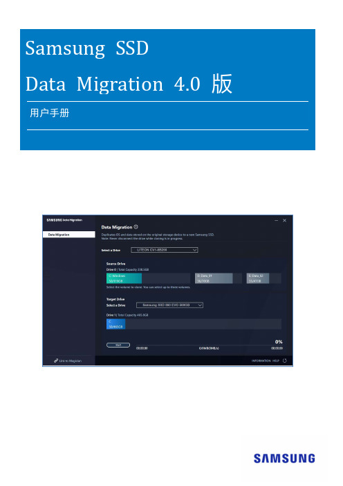
三星电子 Samsung SSD Data Migration 软件用户手册说明书
用户手册版权所有 ©2020三星电子株式会社本用户手册的版权归三星电子所有。
未经授权严格禁止对本资料或其任何部分进行复制、使用或披露,这些行为均违反了版权法。
三星电子保留更改产品、信息和规格的权利,恕不另行通知。
本出版物中提供的材料和信息在出版时被认为是准确且可靠的,但三星电子不保证此处提供的任何材料或信息(无论明示还是暗示)的准确性、完整性或可靠性。
商标和服务标志Samsung徽标是三星电子的商标。
Adobe和 Adobe Acrobat是 Adobe Systems Incorporated的注册商标。
所有其他公司和产品名称可能是其各自公司的商标。
简介Samsung Data Migration软件的设计目的是帮助您迅速、简单、安全地将所有数据从现有的存储设备(如 HD D)迁移到新的 Samsung SSD中。
通过 Samsung Data Migration软件,您可以轻松地将您当前的操作系统、应用程序软件和用户数据迁移到新的 Samsung SSD中。
Samsung Data Migration软件是由 Clonix Co.,Ltd.专为 Samsung Solid State Drive(SSD)的所有者开发和分发的。
注意事项1.在使用本软件克隆源驱动器(如 HDD)的内容时,目标驱动器 (Samsung SSD)上的所有数据将被删除且无法恢复。
因此,如果您希望保留存储在目标驱动器上的任何数据,请提前备份。
2.三星电子对使用本软件造成目标驱动器上的任何数据丢失的情况不承担任何责任,也不负责提供数据恢复服务。
即使克隆失败,源驱动器上存储的数据也不会受到影响。
3.如果您要使用本软件将源驱动器克隆到目标驱动器 (Samsung NVMe TM SSD),请确保首先安装 Samsung NV Me TM驱动程序。
改进功能1.新的型号支持2.克隆兼容性改进系统需求限制1.本软件仅支持用户手册中列出的 Windows操作系统。
- 1、下载文档前请自行甄别文档内容的完整性,平台不提供额外的编辑、内容补充、找答案等附加服务。
- 2、"仅部分预览"的文档,不可在线预览部分如存在完整性等问题,可反馈申请退款(可完整预览的文档不适用该条件!)。
- 3、如文档侵犯您的权益,请联系客服反馈,我们会尽快为您处理(人工客服工作时间:9:00-18:30)。
Samsung Drive Manager
常见问题
安装
问题:我已连接 Samsung 外接硬盘,但系统没有任何反应。
回答:检查 USB 缆线连接。
如果已正确连接 Samsung 外接硬盘,其 LED 应会点亮。
回答:如果硬盘发出滴答声,表明电力不足。
如果当前USB 端口无法识别硬盘,请尝试将它连接到其他 USB 端口。
问题:我无法安装 Samsung Drive Manager。
回答:请检查使用Samsung 外接硬盘的最低系统要求。
有关更多信息,请参阅用户手册第 1 章中的“系统规格”。
问题:我在Windows Vista 上执行Samsung Drive Manager 时,“用户帐户控制”窗口始终显示。
如何才能让“用户帐户控制”窗口不显示?
回答:需要提升权限才能使用Samsung Drive Manager 直接或间接访问外接硬盘。
如果未获得“用户帐户控制”访问权限,则会限制使用
Samsung Drive Manager。
要让“用户帐户控制”窗口不显示,请选择“控制面板”上的“用户帐户”,然后设置“关闭用户帐户控制”。
Samsung AutoBackup
问题:我应该备份哪些东西?
回答:一般来说,应该备份使用其他软件生成的数据文件。
不建议备份程序文件,因为如果计算机出现问题,您必须重新安装这些程序。
建议您备份可以恢复的数据文件。
问题:我应该多长时间备份一次数据?
回答:如果您没有定期备份,建议您备份重要的文件、个人数据(如照片)以及无法重新创建或难于创建的文件。
问题:某些文件已更改,但系统未执行实时备份。
回答:如果更改的文件未设置为备份源,则Samsung AutoBackup 无法执行实时备份。
请确保已将希望实时备份的文件类型设置为实时备份。
回答:另一个原因是,OS 系统文件或文件夹包含在备份源中。
Samsung AutoBackup 无法备份此类由系统使用的文件。
请确保 OS 系统文件夹或文件未包含在备份源中。
问题:我在Windows Vista 或Windows 7 上使用Samsung AutoBackup 时,不会显示备份数据及备份日志。
回答:此问题是由 Windows Vista 版本中的用户帐户控制功能引起的。
已在 Windows XP 上格式化为 NTFS 的 HDD,
在Windows Vista 或Windows 7 上格式化时将不会被授予验证用户的权限。
如果将没有此权限的 HDD 连接到 Windows Vista 或 Windows 7 并使用,则无法正常更新备份数据。
※ FAT32 不会受此问题影响。
问题:我的 Samsung 外接硬盘有足够的空间,但是无法备份超过 2GB 或 4GB 的文件。
回答:可以备份的最大文件大小视Samsung 外接硬盘的文件系统而定。
表 1:文件系统
回答:要备份超过2GB 的文件,您必须将文件系统更改为FAT32 或 NTFS。
要备份超过 4GB 的文件,您必须将文件系统更改为 NTFS。
注意:如果更改文件系统,则 SAMSUNG 外接硬盘上存储的所有数据都会被删除。
在更改文件系统之前,将所有重要数据备
份到其他硬盘。
问题:我已格式化计算机并重新安装了Windows。
如何才能恢复在其他设备上备份的数据?
回答:安装Samsung Drive Manager 并执行Samsung AutoBackup,然后在“作业列表”上选择要恢复的数据。
您可以通过此方式使用备份数据(有关更多信息,请参阅用户手册的第 2 章)。
问题:备份失败后,我在查看备份日志时,发现多项备份失败记录。
回答:备份时无法访问OS 系统文件。
您无法备份OS 系统文件。
在将 Windows 文件夹或“Program Files”文件夹设置为备份源时,通常会出现此问题。
为避免此问题,请勿将整个根文件夹设置为备份源。
仅将用户文件夹设置为备份源。
回答:避免此问题的另一种方法是,将备份失败的文件排除在备份源之外,然后重新执行备份。
问题:我已格式化Samsung 外接硬盘,其中存储的Samsung 软件被删除。
回答:您可以从Samsung 客户支持网站(/sec) 下载Samsung 外接硬盘随附的Samsung 软件。
问题:我备份了安装某种产品时安装的程序。
该产品出现问题时,我删除了程序并恢复了备份的文件,但无法执行该产品。
此备份和恢复过程有什么问题?
回答:所有软件程序都需要在特定环境中执行。
在计算机上安装某个程序时,环境会随程序文件一起安装;在执行该程序时,
系统会检测安装的环境。
由于Samsung AutoBackup 未备份此类环境,因此即使在备份和恢复此类程序后,也无法执行该程序。
问题:运行Samsung AutoBackup 时,我无法使用“安全移除硬件”功能移除Samsung 外接硬盘。
回答:Samsung 外接硬盘在使用时无法安全地移除。
请在关闭Samsung AutoBackup 后再试一次。
问题:文件传输时间太长。
回答:如果您的计算机不支持USB 2.0 或 3.0,或者将Samsung 外接硬盘连接到除USB 2.0 或3.0 端口以外的端口,则会降低文件传输速度。
请将Samsung 外接硬盘连接到支持 USB 2.0 或更高版本的端口。
问题:我无法在 Macintosh 计算机上复制文件。
回答:这可能是文件系统兼容性问题。
如果您的 Samsung 外接硬盘格式化为 NTFS,则只能在 Macintosh 系统上读取保存的数据。
问题:我在备份设备上查看备份文件时,看到一条消息说明“该文件不是正确的格式”和非法文件。
回答:如果已在备份设置中选择加密备份,系统会对文件进行加密和备份。
打开加密文件时,会出现错误,或显示一条消息说明“该文件不是正确的格式”。
必须先恢复加密文件,然后才能打开该文件。
问题:在启用“加密”选项的情况下,我执行了备份。
但仅加密了选定文件。
回答:仅对启用“加密”后备份的文件进行加密和备份,而不会对启用“加密”前备份的文件进行加密。
这意味着已加密的文件和未加密的文件可以存在于相同备份设备上。
问题:是否可以将包含备份数据的 Samsung 外接硬盘连接到其他计算机并恢复备份数据?如果可以,应该怎么做?
回答:要恢复和使用从其他计算机备份的数据,请将Samsung 外接硬盘连接到计算机并安装Samsung Drive Manager,然后执行Samsung Auto Backup 并选择要恢复的备份文件。
问题:如何才能检查备份、恢复或删除操作的结果?
回答:在备份、恢复或删除操作完成后,您可以在Samsung AutoBackup 屏幕的作业菜单上显示的“日志”中查看结果。
Samsung SecretZone
问题:如何才能保护我的安全驱动器不被其他用户访问?
回答:在Samsung SecretZone 上选择要保护的图像,然后选择“断开连接”。
在管理员选择“连接”后,其他用户才能查看安全驱动器。
问题:在重新安装 OS 后,如何才能重新使用安全驱动器?
回答:要在重新安装OS 后重新使用安全驱动器,请重新安装Samsung Drive Manager,连接Samsung 外接硬盘,选择要在Samsung SecretZone 中使用的安全驱动器,然后单击“连接”。
问题:安全驱动器最大大小是多少?
回答:安全驱动器大小可以和 Samsung 外接硬盘上的可用空间一样大。
问题:忘记密码应该怎么办?
回答: Samsung SecretZone 是一种安全程序,如果没有正确的密码,则不能使用安全驱动器。
请确保您为安全驱动器设置的密码容易记住。
问题:运行Samsung SecretZone 时,我无法使用“安全移除硬件”功能移除Samsung 外接硬盘。
回答:断开当前正在运行的所有安全驱动器,关闭Samusng SecretZone,然后安全地移除 Samsung 外接硬盘。
问题:在安全驱动器上启用“自动连接”后,驱动器未连接。
回答:视 PC 规格而定,连接 Samsung 外接硬盘可能需要一些时间。
请稍等片刻,直到建立连接。
问题:断开安全驱动器的连接时显示错误消息。
回答:如果在复制或保存大文件或多个文件后立即断开安全驱动器的连接,可能会出现错误。
如果出现错误,请在30 秒到 1 分钟后再试一次。
Samsung Secure Manager
问题:我是否可以在未安装Samsung Drive Manager 的情况下解锁 Samsung 安全硬盘?
回答:连接Samsung 安全硬盘,执行“我的电脑”中显示的CD 驱动器中的Secure Unlocker_win.exe,然后输入解锁密码。
A. 您必须在 Macintosh 上执行 Secure Unlock_mac.app。
问题:什么是恢复出厂设置功能?
回答:恢复出厂设置功能可删除安全硬盘上保存的所有数据,并可恢复默认安全设置。