SOT-89-3L三极管封装尺寸
BCX53贴片三极管 SOT-89三极管封装BCX53参数

CLASSIFICATION OF hFE(2)
RANK
BCX51 BCX52 BCX53
RANGE
63–250
BCX51-10 BCX52-10 BCX53-10
63–160
BCX51-16 BCX52-16 BCX53-16
100–250
C,Sep,2012
Typical Characteristics
Parameter
Collector-base breakdown voltage
Collector-emitter breakdown voltage
Emitter-base breakdown voltage Collector cut-off current Emitter cut-off current
4.600
1.550 REF.
2.300
2.600
3.940
4.250
1.500 TYP.
3.000 TYP.
0.900
1.200
Dimensions In Inches
Min.
Max.
0.055
0.063
0.013
0.020
0.016
0.023
0.014
0.017
0.173
0.181
0.061 REF.
FE
C
T =100 oC a
T =25 oC a
10 -1
-400
β=10
-300
-10
-100
COLLECTOR CURRENT I (mA) C
V —— I
CEsat
C
-1000
-200 -100
2SC2881贴片三极管 SOT-89封装三极管2SC2881参数
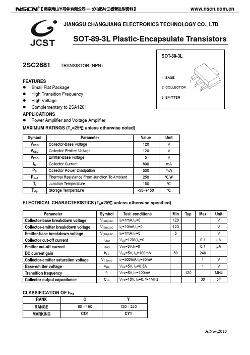
A,Nov,2010JIANGSU CHANGJIANG ELECTRONICS TECHNOLOGY CO., LTDSOT-89-3L Plastic-Encapsulate Transistors2SC2881 TRANSISTOR (NPN) FEATURES z Small Flat Package z High Transition Frequency z High Voltagez Complementary to 2SA1201 APPLICATIONSz Power Amplifier and Voltage AmplifierMAXIMUM RATINGS (T a =25℃ unless otherwise noted)ELECTRICAL CHARACTERISTICS (T a =25℃ unless otherwise specified)ParameterSymbol Test conditions Min Typ Max Unit Collector-base breakdown voltageV (BR)CBO I C =1mA,I E =0 120 V Collector-emitter breakdown voltageV (BR)CEO I C =10mA,I B =0 120 V Emitter-base breakdown voltageV (BR)EBO I E =1mA,I C =0 5 V Collector cut-off currentI CBO V CB =120V,I E =0 0.1 µA Emitter cut-off currentI EBO V EB =5V,I C =0 0.1 µA DC current gainh FE V CE =5V, I C =100mA 80 240 Collector-emitter saturation voltageV CE(sat) I C =500mA,I B =50mA1 V Base-emitter voltageV BE V CE =5V, I C =0.5A 1 V Transition frequencyf T V CE =5V,I C =100mA 120 MHz Collector output capacitanceC ob V CB =10V, I E =0, f=1MHz 30 pFCLASSIFICATION OF h FERANKO Y RANGE80–160 120–240 MARKINGCO1 CY1Symbol Parameter Value Unit V CBOCollector-Base Voltage 120 V V CEOCollector-Emitter Voltage 120 V V EBOEmitter-Base Voltage 5 V I CCollector Current 800 mA P CCollector Power Dissipation 500 mW R θJAThermal Resistance From Junction To Ambient 250 ℃/W T jJunction Temperature 150 ℃ T stg Storage Temperature -55~+150 ℃ 【南京南山半导体有限公司 — 长电贴片三极管选型资料】【Label on the Inner Box Label on the Outer BoxQA LabelSeal the boxwith the tapeSeal the boxwith the tapeStamp “EMPTY”on the empty boxInner Box: 210 mm× 208mm×203 m m Outer Box: 440 mm× 440mm× 230mmThe top gasket1000×1 PCSLabel on the ReelThe bottom gasketThe file folderPlastic bag。
A44贴片三极管 SOT-89三极管封装A44参数

C ,Jun ,2013JIANGSU CHANGJIANG ELECTRONICS TECHNOLOGY CO., LTDSOT-89-3L Plastic-Encapsulate TransistorsA44 TRANSISTOR (NPN) FEATURES z Low Collector-Emitter Saturation Voltage z High Breakdown VoltageMARKING: A44MAXIMUM RATINGS (T a =25℃ unless otherwise noted)ELECTRICAL CHARACTERISTICS (Ta =25℃ unless otherwise specified)ParameterSymbol T est conditions Min Typ MaxUnit Collector-base breakdown voltageV (BR)CBO I C =100µA,I E =0 400 V Collector-emitter breakdown voltageV (BR)CEO *I C =1mA,I B =0 400 V Emitter-base breakdown voltageV (BR)EBO I E =10µA,I C =0 6 V Collector cut-off currentI CBO V CB =400V,I E =0 0.1 µA Emitter cut-off current I EBOV EB =4V,I C =0 0.1 µA h FE(1)* V CE =10V, I C =1mA 40h FE(2)* V CE =10V, I C =10mA 50200 h FE(3)* V CE =10V, I C =50mA 45DC current gain h FE(4)* V CE =10V, I C =100mA 40 I C =1mA,I B =0.1mA 0.4 VI C =10mA,I B =1mA 0.5 V Collector-emitter saturation voltageV CE(sat)* I C =50mA,I B =5mA 0.75 V Base-emitter saturation voltageV BE(sat)* I C =10mA,I B =1mA 0.75 V Collector output capacitanceC ob V CB =20V, I E =0, f=1MHz 7 pF Emitter input capacitance C ib V BE =0.5V, I C =0, f=1MHz 130 pF *Pulse test: pulse width ≤300μs, duty cycle ≤ 2.0%.I CCollector Current -Continuous 200mA P CCollector Power Dissipation 500 mW R θJAThermal Resistance f rom Junction t o Ambient 250℃/W T jJunction Temperature 150 ℃ T stg Storage Temperature -55~+150 ℃ I CMCollector Current -Pulsed 300 mA 【南京南山半导体有限公司 — 长电贴片三极管选型资料】【Label on the Inner Box Label on the Outer BoxQA LabelSeal the boxwith the tapeSeal the boxwith the tapeStamp “EMPTY”on the empty boxInner Box: 210 mm× 208mm×203 m m Outer Box: 440 mm× 440mm× 230mmThe top gasket1000×1 PCSLabel on the ReelThe bottom gasketThe file folderPlastic bag。
2SD1616A贴片三极管 SOT-89封装三极管2SD1616A参数
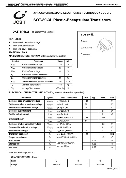
JIANGSU CHANGJIANG ELECTRONICS TECHNOLOGY CO., LTDSOT-89-3L Plastic-Encapsulate Transistors2SD1616ATRANSISTOR (NPN ) FEATURES MARKING:1616Az Low collector saturation voltage z High break down voltagez High total power dissipation MAXIMUM RATINGS (T a =25℃ unless otherwise noted) Symbol Parameter ValueUnit V CBOCollector-Base Voltage 120 V V CEOCollector-Emitter Voltage 60 V V EBOEmitter-Base Voltage 6 V I CCollector Current -Continuous 1 A P CCollector Power Dissipation 0.5 W R ӨJAThermal Resistance, junction to Ambient 250 ℃/W T jJunction Temperature 150 ℃ T stg Storage Temperature -55~+150℃ ELECTRICAL CHARACTERISTICS (Ta=25℃ unless otherwise specified)*pulse test: PW ≤350µs , δ≤2%. CLASSIFICATION of h FE1Rank L K URange 135-270 200-400 300-600 Parameter Symbol Test conditions M in T ypM ax Unit Collector-base breakdown voltageV (BR)CBO I C =10μA , I E =0 120 V Collector-emitter breakdown voltageV (BR)CEO I C =2mA , I B =0 60 V Emitter-base breakdown voltageV (BR)EBO I E =10μA, I C =0 6 V Collector cut-off currentI CBO V CB =60V, I E =0 0.1 μA Emitter cut-off currentI EBO V EB =6V, I C =0 0.1 μA h FE1 V CE =2V, I C =100mA 135 600 DC current gain*h FE2 V CE =2V, I C =1A 81 Collector-emitter saturation voltage *V CE(sat) I C = 1A, I B =50mA 0.3 V Base-emitter saturation voltage *V BE(sat) I C = 1A, I B =50mA 1.2 V Base-emitter voltage *V BE V CE = 2V, I C =50mA 0.6 0.7 V Transition frequencyf T V CE =2V, I C = 100mA 100 MHz Output capacitanceC ob V CB =10 V,I E = 0, f=1MHz 19 pF Turn on timet on 0.07 μs Storage timet S 0.95 μs Fall timet F Vcc=10V, I C =100mA, I B1=-I B2=10mA 0.07 μsSOT-89-3L 1. BASE 2. COLLETOR 3. EMITTER B,Feb,2013【南京南山半导体有限公司 — 长电贴片三极管选型资料】【Label on the Inner Box Label on the Outer BoxQA LabelSeal the boxwith the tapeSeal the boxwith the tapeStamp “EMPTY”on the empty boxInner Box: 210 mm× 208mm×203 m m Outer Box: 440 mm× 440mm× 230mmThe top gasket1000×1 PCSLabel on the ReelThe bottom gasketThe file folderPlastic bag。
2SA1013贴片三极管 SOT-89封装三极管2SA1013参数

The bottom gasket
The file folder
Label on the Reel Plastic bag 1000×1 PCS
The top gasket
Seal the box with the tape
Stamp “EMPTY” on the empty box
Seal the box with the tape
Dimensions In Inc 0.016 0.023 0.014 0.017 0.173 0.181 0.061 REF. 0.091 0.102 0.155 0.167 0.060 TYP. 0.118 TYP. 0.035 0.047
fT
CLASSIFICATION OF hFE Rank Range R 60-120 O 100-200 Y 160-320
A,Mar,2011
【 南京南山半导体有限公司 — 长电三极管选型资料】
Symbol A b b1 c D D1 E E1 e e1 L
Dimensions In Millimeters Min. Max. 1.400 1.600 0.320 0.520 0.400 0.580 0.350 0.440 4.400 4.600 1.550 REF. 2.300 2.600 3.940 4.250 1.500 TYP. 3.000 TYP. 0.900 1.200
QA Label
Label on the Inner Box Inner Box: 210 mm× 208 mm×203 mm
Label on the Outer Box Outer Box: 440 mm× 440 mm× 230 mm
1. BASE
KTC4379贴片三极管 SOT-89三极管封装KTC4379参数
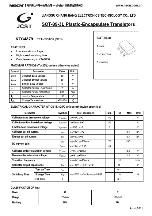
JIANGSU CHANGJIANG ELECTRONICS TECHNOLOGY CO., LTDSOT-89-3L Plastic-Encapsulate TransistorsKTC4379 TRANSISTOR (NPN) FEATURES z Low saturation voltagez High speed switching time z Complementary to KTA1666 MAXIMUM RATINGS (T a =25℃ unless otherwise noted)ELECTRICAL CHARACTERISTICS (T a =25℃ unless otherwise specified)ParameterSymbol Test conditions M in T yp Max Unit Collector-base breakdown voltageV (BR)CBO I C =1mA, I E =0 50 V Collector-emitter breakdown voltageV (BR)CEO I C =10mA, I B =0 50 V Emitter-base breakdown voltageV (BR)EBO I E =1mA, I C =0 5 V Collector cut-off currentI CBO V CB =50V, I E =0 0.1 μA Emitter cut-off currentI EBO V EB =5V, I C =0 0.1 μA h FE(1) V CE =2V, I C =500mA 70 240 DC current gainh FE(2) V CE =2V, I C = 1.5A 40 Collector-emitter saturation voltageV CE(sat) I C =1A, I B =50mA 0.5 V Base-emitter saturation voltageV BE(sat) I C =1A, I B =50mA 1.2 V Transition frequencyf T V CE =2V, I C =500mA 120 MHz Collector output capacitanceC ob V CB =10V, I E =0, f=1MHz 30 pF Turn on Timet on 0.1 Storage Timet stg 1.0 Switching Time Fall Time t f V CC =30V, I C =1A, I B1=-I B2=-0.05A 0.1μsCLASSIFICATION OF h FE(1)Rank OY Range 70-140 120-240 Marking UO UYSOT-89-3L 1. BASE 2. COLLECTOR 3. EMITTER A,Jun,2011【南京南山半导体有限公司 — 长电贴片三极管选型资料】【Label on the Inner Box Label on the Outer BoxQA LabelSeal the boxwith the tapeSeal the boxwith the tapeStamp “EMPTY”on the empty boxInner Box: 210 mm× 208mm×203 m m Outer Box: 440 mm× 440mm× 230mmThe top gasket1000×1 PCSLabel on the ReelThe bottom gasketThe file folderPlastic bag。
KTC4373贴片三极管 SOT-89三极管封装KTC4373参数
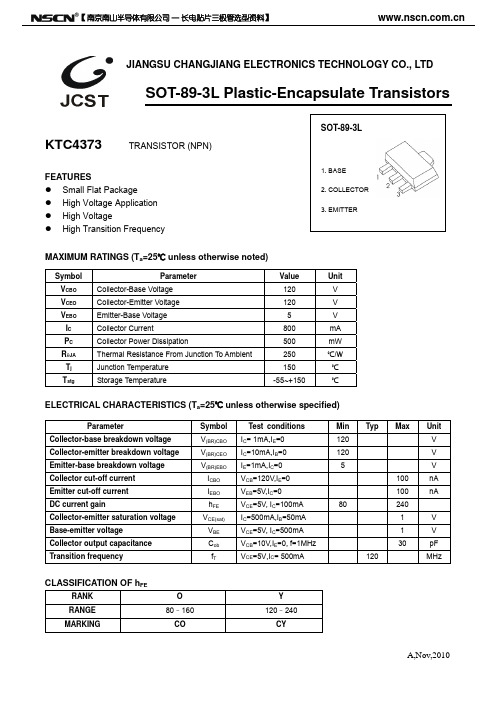
A,Nov,2010JIANGSU CHANGJIANG ELECTRONICS TECHNOLOGY CO., LTDSOT-89-3L Plastic-Encapsulate TransistorsKTC4373 TRANSISTOR (NPN) FEATURES z Small Flat Package z High Voltage Application z High Voltagez High Transition FrequencyMAXIMUM RATINGS (T a =25℃ unless otherwise noted)ELECTRICAL CHARACTERISTICS (T a =25℃ unless otherwise specified)ParameterSymbol Test conditions Min Typ Max Unit Collector-base breakdown voltageV (BR)CBO I C = 1mA,I E =0 120 V Collector-emitter breakdown voltageV (BR)CEO I C =10mA,I B =0 120 V Emitter-base breakdown voltageV (BR)EBO I E =1mA,I C =0 5 V Collector cut-off currentI CBO V CB =120V,I E =0 100 nA Emitter cut-off currentI EBO V EB =5V,I C =0 100 nA DC current gainh FE V CE =5V, I C =100mA 80 240 Collector-emitter saturation voltageV CE(sat)I C =500mA,I B =50mA 1 V Base-emitter voltageV BE V CE =5V, I C =500mA 1 V Collector output capacitanceC ob V CB =10V,I E =0, f=1MHz 30 pF Transition frequency f T V CE =5V,I C = 500mA 120 MHzCLASSIFICATION OF h FERANKO Y RANGE80–160 120–240 MARKINGCO CYSymbol Parameter Value Unit V CBOCollector-Base Voltage 120 V V CEOCollector-Emitter Voltage 120 V V EBOEmitter-Base Voltage 5 V I CCollector Current 800 mA P CCollector Power Dissipation 500 mW R θJAThermal Resistance From Junction To Ambient 250 ℃/W T jJunction Temperature 150 ℃ T stg Storage Temperature -55~+150 ℃ 【南京南山半导体有限公司 — 长电贴片三极管选型资料】【Label on the Inner Box Label on the Outer BoxQA LabelSeal the boxwith the tapeSeal the boxwith the tapeStamp “EMPTY”on the empty boxInner Box: 210 mm× 208mm×203 m m Outer Box: 440 mm× 440mm× 230mmThe top gasket1000×1 PCSLabel on the ReelThe bottom gasketThe file folderPlastic bag。
2SD2150贴片三极管 SOT-89三极管封装2SD2150参数
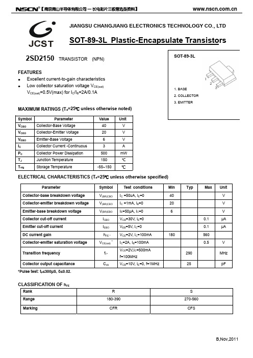
JIANGSU CHANGJIANG ELECTRONICS TECHNOLOGY CO., LTDSOT-89-3L Plastic-Encapsulate Transistors2SD2150 TRANSISTOR (NPN)FEATURES z Excellent current-to-gain characteristics zLow collector saturation voltage V CE(sat) V CE(sat)=0.5V(max) for I C /I B =2A/0.1A MAXIMUM RATINGS (T a =25℃ unless otherwise noted) ELECTRICAL CHARACTERISTICS (T a =25℃ unless otherwise specified) ParameterSymbol Test conditions M in Typ Max Unit Collector-base breakdown voltageV (BR)CBO I C =50uA, I E =0 40 V Collector-emitter breakdown voltageV (BR)CEO I C =1mA, I B =0 20 V Emitter-base breakdown voltageV (BR)EBO I E =50μA, I C =0 6 V Collector cut-off currentI CBO V CB =30V, I E =0 0.1 μA Emitter cut-off currentI EBO V EB =5V, I C =0 0.1 μA DC current gainh FE * V CE =2V, I C =100mA 180 560 Collector-emitter saturation voltageV CE(sat) * I C =2A, I B =100mA 0.5 V Transition frequencyf T* V CE =2V,I C =500mA f=100MHz 290 MHz Collector output capacitanceC ob V CB =10V, I E =0, f=1MHz 25 pF*Pulse test: t p ≤300μS, δ≤0.02.CLASSIFICATION OF h FERankR S Range180-390 270-560 Marking CFR CFSSOT-89-3L 1. BASE 2. COLLECTOR 3. EMITTER B,Nov,2011【南京南山半导体有限公司 — 长电贴片三极管选型资料】200400600800100012000.1110100100010100408012016020002550751001251503000BA S E -E M I T T E R S A T U R A T I O NV O L T AG EV BE sa t(m V)I h ——CO L L C E T O R C U R R E N T I C(m A )500T RAN SI T I ONFR EQ UEN C YfT(M H z )COLLECTOR CURRENT I C (mA) 2SD2150Static Characteristic C O L L E C T O R C U R R E N T I C(m A )Typical Characteristics AMBIENT TEMPERATURE T a ()℃ B,Nov,2011【Label on the Inner Box Label on the Outer BoxQA LabelSeal the boxwith the tapeSeal the boxwith the tapeStamp “EMPTY”on the empty boxInner Box: 210 mm× 208mm×203 m m Outer Box: 440 mm× 440mm× 230mmThe top gasket1000×1 PCSLabel on the ReelThe bottom gasketThe file folderPlastic bag。
- 1、下载文档前请自行甄别文档内容的完整性,平台不提供额外的编辑、内容补充、找答案等附加服务。
- 2、"仅部分预览"的文档,不可在线预览部分如存在完整性等问题,可反馈申请退款(可完整预览的文档不适用该条件!)。
- 3、如文档侵犯您的权益,请联系客服反馈,我们会尽快为您处理(人工客服工作时间:9:00-18:30)。
Min.Max.Min.Max.
A1.4001.6000.0550.063
b0.3200.5200.0130.020
b10.4000.5800.0160.023
c0.3500.4400.0140.017
D4.4004.6000.1730.181
D1
E2.3002.6000.0910.102
E13.9404.2500.1550.167
ee1L0.9001.2000.0350.0473.000 TYP.0.118 TYP.SymbolDimensions In MillimetersDimensions In Inches1.550 REF.0.061 REF.1.500 TYP.0.060 TYP.
www.nscn.com.cn
【
南京南山半导体有限公司 — 长电三极管选型资料
】
Label on the Inner Box Label on the Outer Box
QA Label
Seal the box
with the tape
Seal the box
with the tape
Stamp “EMPTY”
on the empty box
Inner Box:
210 mm× 208 mm×203 mmOuter Box: 440 mm× 440 mm× 230 mm
The top gasket
1000×1 PCS
Label on the Reel
The bottom gasket
The file folder
Plastic bag