SN74AVC16T245(16位双向传输电平转换器)
DSP常见问题解答
DSP常见问题解答如何选择外部时钟?DSP的内部指令周期较高,外部晶振的主频不够,因此DSP大多数片内均有PLL。
但每个系列不尽相同。
1)TMS320C2000系列:TMS320C20x:PLL可以÷2,×1,×2和×4,因此外部时钟可以为5MHz-40MHz。
TMS320F240:PLL可以÷2,×1,×1.5,×2,×2.5,×3,×4,×4.5,×5和×9,因此外部时钟可以为2.22MHz-40MHz。
TMS320F241/C242/F243:PLL可以×4,因此外部时钟为5MHz。
TMS320LF24xx:PLL可以由RC调节,因此外部时钟为4MHz-20MHz。
TMS320LF24xxA:PLL可以由RC调节,因此外部时钟为4MHz-20MHz。
2)TMS320C3x系列:TMS320C3x:没有PLL,因此外部主频为工作频率的2倍。
TMS320VC33:PLL可以÷2,×1,×5,因此外部主频可以为12MHz -100MHz。
3)TMS320C5000系列:TMS320VC54xx:PLL可以÷4,÷2,×1-32,因此外部主频可以为0.625MHz-50MHz。
TMS320VC55xx:PLL可以÷4,÷2,×1-32,因此外部主频可以为6.25MHz-300MHz。
4)TMS320C6000系列:TMS320C62xx:PLL可以×1,×4,×6,×7,×8,×9,×10和×11,因此外部主频可以为11.8MHz-300MHz。
TMS320C67xx:PLL可以×1和×4,因此外部主频可以为12.5MHz-230MHz。
74HC245电路

细的参数规格及各厂商型号替换,请以厂商数据手册为准。
生产工艺
TI 公司
ON 公司
工作电压(V)
输入电平兼容
输出电平兼容
74F
F
4.5~5.5
TTL
TTL
Bipolar 5V-Logic
LS
LS
4.75~5.25
TTL
TTL
ALS
4.5~5.5
TTL
TTL
CD4000 系列
MC1400 系列
3.0~18
DFT2,XV5T2
DTT1,DFT2
US
z 工业级温度范围: -40~85℃
07
Buffer OD
DFT2,XV5T2
DTT1,DFT2
US
08
2-Input AND
DFT2,XV5T2
US
14
Inverter-Schmitt
DFT2,XV5T2
DTT1,DFT2
US
数
优点
16
Buffer
DFT2,XV5T2
150
产品参数仅供参考,以厂家数据手册为准。批量价格,欢迎垂询。更多详情:
免费业务电话:800-880-8051 总机:027-8752 6752 传真:027-8752 6551
CMOS
CMOS
HC
HC
2.0~6.0
CMOS
CMOS
AHC
VHC
2.0~5.5
CMOS
CMOS
AHC1G
MC74VHC1G
2.0~6.0
CMOS
CMOS
CMOS 5V-Logic
HCT
HCT
4.5~5.5
74lvc245中文说明
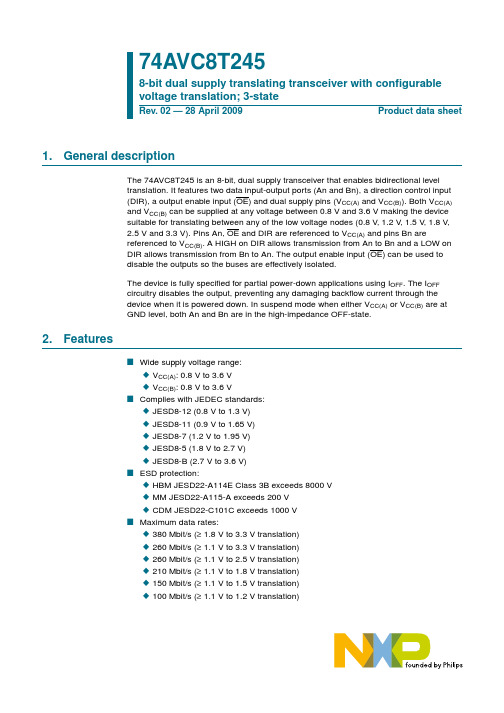
74LV245是低压硅栅CMOS器件,与74HC245和74HCT245针脚和功能兼容。
74LV245是八位元收发器,在发送和接收方向上都具有非反相3态总线兼容输出。
发送/接收(DIR)输入控制方向,而输出使能(OE)输入则可实现轻松级联。
针脚OE控制输出,因此总线可以得到有效隔离。
特性和优势
•宽工作电压范围:1.0 V至5.5 V
•最适合低压应用:1.0 V至3.6 V
•接受介于VCC = 2.7 V和VCC = 3.6 V之间的TTL输入电平
•VCC = 3.3 V且T amb = 25 °C时的典型输出地弹:< 0.8 V
•VCC = 3.3 V且T amb = 25 °C时的典型高电平输出电压(VOH)欠冲:> 2 V •ESD保护:
o HBM JESD22-A114E超过2000 V
o MM JESD22-A115-A超过200 V
•多种封装选择
•额定温度范围为-40 °C至+85 °C和-40 °C至+125 °C
外形图
显示功能框图
真值表
INPUTS INPUTS/OUTPUT OE DIR An Bn
H=高电压L=低电压X=无输入、Z=高阻态。
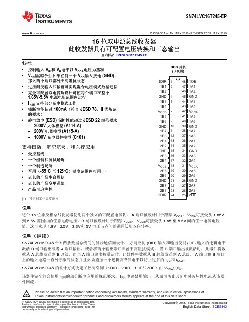
74AVC8T245 8位数据双向电平转换IC
Supply voltage
Input
VCC(A), VCC(B) 0.8 V to 3.6 V
OE[2] L
0.8 V to 3.6 V
L
0.8 V to 3.6 V
H
GND[3]
X
DIR[2] L H X X
Input/output[3] An[2] An = Bn input Z Z
[1] H = HIGH voltage level; L = LOW voltage level; X = don’t care; Z = high-impedance OFF-state. [2] The An, DIR and OE input circuit is referenced to VCC(A); The Bn input circuit is referenced to VCC(B). [3] If at least one of VCC(A) or VCC(B) is at GND level, the device goes into suspend mode.
NXP Semiconductors
74AVC8T245
8-bit dual supply translating transceiver; 3-state
I Suspend mode I Latch-up performance exceeds 100 mA per JESD 78 Class II I Inputs accept voltages up to 3.6 V I IOFF circuitry provides partial Power-down mode operation I Multiple package options I Specified from −40 °C to +85 °C and −40 °C to +125 °C
德尔福汽车仪表拆解报告+结构设计update

德尔福汽车仪表拆解报告1、汽车仪表后盖图后盖上可以看到电源及总线接口以及预留RGB串行化显示的接口。
2、卸掉后盖螺丝之后,可以看到PCB的正反面全貌,整体比较整洁,采用一块PCB 板,所有的元器件采用类似苹果产品的方法,去掉了丝印。
正面反面3、整机的ESD及结构设计无论是PCB还是外壳,我们可以看到,ESD设计非常好,主机板的放电回路无论是正面还是反面都通过8个螺丝孔与外壳充分的接触。
ESD放电螺丝孔金属垫片设计LED指示灯并非传统的通过排线引出PCB的设计,而是采用导光槽,LED光通过导光槽之后,均匀的投射到碳膜指示区域。
LED导光槽设计4、整机硬件架构分析1)CPU:Freescale i.mx51车规级芯片(MCIMX514AJM6C)主频:600MH z2) DDR: micron DDR2 256M3) eMMC: ST 16G4) Norflash: Spanion 256M5) 电源方案:B+电源方案:B+电源进入之后的方案较为简单,通过两个防反接的二极管之后,分别使用了2颗470UF的铝电解和一颗cooper的电感,具体参数如下。
DRA 系列磁性屏蔽磁鼓芯电感器,具有高功率密度和高效性,适用于汽车应用。
DRA 系列电感器设计带有铁氧体磁芯,可牢固安装,适用于高冲击和振动环境。
DRA 系列的应用包括:汽车电子(用于罩盖下,内部/外部);车载信息服务;直流到直流转换器;降压、升压、正向和谐振转换器;噪音过滤和滤波器扼流圈,165°C 最高工作温度。
第一级电源方案(12V降压到5V):一部分提供给MCU工作,另外一部分提供给其他的DC/DC电源作为输入电源TPS54362 车规级电源芯片。
3A,可耐压为60V,规格书开关频率为:200K~2.2MHz。
德尔福设置开关频率为500KHz,输入端都采用了470UF的nichicon的铝电解电容。
CPU及周边供电:使用了两颗车规级芯片TPS65023:3路DC/DC 系统供电3.3V,memory供电1.8V,CPU供电 1.2V3路DC/DC CPU供电2.775V,CPU供电1.05V,一路NC开关频率固定为2.25Mhz,在power save状态下,可以依据负载电流的不同而在750K到2.25MHz之间变化。
sn74lvc16t245-(适合国防与航空航天)
1 2 3 4 5 6 7 8 9 10 11 12 13 14 15 16 17 18 19 20 21 22 23 2448 47 46 45 44 43 42 41 40 39 38 37 36 35 34 33 32 31 30 29 28 27 26 251DIR 1B1 1B2 GND 1B3 1B4 V CCB 1B5 1B6 GND 1B7 1B8 2B1 2B2 GND 2B3 2B4 V CCB 2B5 2B6 GND 2B7 2B8 2DIR1OE1A11A2GND1A31A4V CCA1A51A6GND1A71A82A12A2GND2A32A4V CCA2A52A6GND2A72A82OESN74LVC16T245-EP ZHCSAQ3A–JANUARY2013–REVISED FEBRUARY201316位双电源总线收发器此收发器具有可配置电压转换和三态输出查询样品:SN74LVC16T245-EP特性DGG封装•控制输入V IH和V IL电平以V CCA电压为基准(顶视图)•V CC隔离特性-如果任何一个V CC输入接地(GND),那么两个端口都处于高阻抗状态•过压耐受输入和输出可实现混合电压模式数据通信•完全可配置双电源轨设计可使每个端口在整个1.65V-5.5V电源电压范围内运行•I关闭支持部分断电模式工作•锁断性能超过100mA(符合JESD78,II类规范的要求)•静电放电(ESD)保护性能超过JESD22规范要求–2000V人体模型(A114-A)–200V机器模型(A115-A)–1000V充电器件模型(C101)支持国防、航空航天、和医疗应用•受控基线•一个组装和测试场所•一个制造场所•军用(-55°C至125°C)温度范围内可用(1)•延长的产品生命周期•延长的产品变更通知•产品可追溯性(1)可定制工作温度范围说明这个16位非反相总线收发器使用两个独立的可配置电源轨。
75HC245规格书
1.General descriptionThe 74HC245; 74HCT245 is a high-speed Si-gate CMOS device and is pin compatible with Low-Power Schottky TTL (LSTTL).The 74HC245; 74HCT245 is an octal transceiver featuring non-inverting 3-state bus compatible outputs in both send and receive directions. The 74HC245; 74HCT245features an output enable input (OE) for easy cascading and a send/receive input (DIR)for direction control.OE controls the outputs so that the buses are effectively isolated.The 74HC245; 74HCT245 is similar to the 74HC640; 74HCT640 but has true (non-inverting) outputs.2.Featuress Octal bidirectional bus interface s Non-inverting 3-state outputs s Multiple package optionss Complies with JEDEC standard no. 7A sESD protection:x HBM EIA/JESD22-A114-B exceeds 2000V x MM EIA/JESD22-A115-A exceeds 200Vs Specified from −40°C to +85°C and from −40°C to +125°C3.Quick reference data74HC245; 74HCT245Octal bus tranceiver; 3-stateRev. 03 — 31 January 2005Product data sheetTable 1:Quick reference data GND =0V; T amb =25°C; t r =t f =6 ns.Symbol ParameterConditions Min Typ Max Unit Type 74HC245t PHL , t PLH propagation delay An to Bn or Bn to An C L =15pF;V CC =5V-7-ns C I input capacitance - 3.5-pF C I/O input/output capacitance -10-pF C PDpower dissipation capacitance per transceiverV I =GND to V CC[1]-30-pFType 74HCT245t PHL , t PLHpropagation delay An to Bn or Bn to AnC L =15pF;V CC =5V-10-ns[1]C PD is used to determine the dynamic power dissipation (P D in µW):P D =C PD ×V CC 2×f i ×N +∑ (C L ×V CC 2×f o ) where:f i =input frequency in MHz;f o =output frequency in MHz;C L =output load capacitance in pF;V CC =supply voltage in V;N =number of inputs switching;∑(C L ×V CC 2×f o )=sum of outputs.4.Ordering informationC I input capacitance - 3.5-pF C I/O input/output capacitance -10-pF C PDpower dissipation capacitance per transceiverV I =GND to V CC −1.5V[1]-30-pFTable 1:Quick reference data …continued GND =0V; T amb =25°C; t r =t f =6 ns.Symbol Parameter Conditions Min Typ Max Unit Table 2:Ordering informationType numberPackageTemperature range NameDescriptionVersion 74HC245N −40°C to +125°C DIP20plastic dual in-line package; 20leads (300 mil)SOT146-174HC245D −40°C to +125°C SO20plastic small outline package; 20leads;body width 7.5mmSOT163-174HC245PW −40°C to +125°C TSSOP20plastic thin shrink small outline package; 20leads;body width 4.4mmSOT360-174HC245DB −40°C to +125°C SSOP20plastic shrink small outline package; 20leads;body width 5.3mmSOT339-174HC245BQ−40°C to +125°CDHVQFN20plastic dual-in-line compatible thermal enhanced very thin quad flat package no leads;20terminals;body 2.5×4.5×0.85mm SOT764-174HCT245N −40°C to +125°C DIP20plastic dual in-line package; 20leads (300 mil)SOT146-174HCT245D −40°C to +125°C SO20plastic small outline package; 20leads;body width 7.5mmSOT163-174HCT245PW −40°C to +125°C TSSOP20plastic thin shrink small outline package; 20leads;body width 4.4mmSOT360-174HCT245DB −40°C to +125°C SSOP20plastic shrink small outline package; 20leads;body width 5.3mmSOT339-174HCT245BQ−40°C to +125°CDHVQFN20plastic dual-in-line compatible thermal enhanced very thin quad flat package no leads;20terminals;body 2.5×4.5×0.85mmSOT764-15.Functional diagramFig 1.Logic symbol Fig 2.IEC logic symbol21DIR1819B0B1B2B3B4B5B6B73174165156147138129A0A1A2A3A4A5A6A711OEmna1741731192116415514613712811918G33EN13EN22mna1756.Pinning information6.1Pinning6.2Pin description(1)The die substrate is attached to thispad using conductive die attachmaterial. It can not be used as supply pin or inputFig 3.Pin configuration DIP20, SO20,SSOP20 and TSSOP20Fig 4.Pin configuration DHVQFN20245DIR V CC A0OE A1B0A2B1A3B2A4B3A5B4A6B5A7B6GND B7001aac4311234567891012111413161518172019001aac432245GND (1)Transparent top viewB6A6A7B5A5B4A4B3A3B2A2B1A1B0A0OE G N D B 7D I RV C C9128137146155164173182191011120terminal 1index areaTable 3:Pin descriptionSymbol Pin Description DIR 1direction control A02data input/output A13data input/output A24data input/output A35data input/output A46data input/output A57data input/output A68data input/output A79data input/output GND 10ground (0V)B711data input/output B612data input/output B513data input/output B414data input/output B315data input/output B216data input/output7.Functional description7.1Function table[1]H =HIGH voltage level;L =LOW voltage level;X =don’t care;Z =high-impedance OFF-state.8.Limiting values[1]For DIP20 packages: above 70°C, P tot derates linearly with 12mW/K.For SO20 packages: above 70°C, P tot derates linearly with 8mW/K.For SSOP20 and TSSOP20 packages: above 60°C, P tot derates linearly with 5.5mW/K.For DHVQFN20 packages: above 60°C, P tot derates linearly with 4.5mW/K.B117data input/output B018data input/outputOE 19output enable input (active LOW)V CC20supply voltageTable 3:Pin description …continuedSymbol Pin Description Table 4:Function table [1]Input Input/outputOE DIR An Bn L L A = B input L H input B = A HXZZTable 5:Limiting valuesIn accordance with the Absolute Maximum Rating System (IEC 60134). Voltages are referenced to GND (ground = 0 V).Symbol Parameter ConditionsMin Max Unit V CC supply voltage −0.5+7V I IK input diode current V I <−0.5V or V I >V CC +0.5 V -±20mA I OK output diode current V O <−0.5V or V O >V CC +0.5V-±20mA I O output source or sink currentV O =−0.5V to V CC +0.5V-±35mA I CC , I GND V CC or GND current -±70mA T stg storage temperature −65+150°C P tottotal power dissipation [1]DIP20 package -750mW SO20, SSOP20,TSSOP20 andDHVQFN20 packages-500mW9.Recommended operating conditions10.Static characteristicsTable 6:Recommended operating conditions Symbol Parameter ConditionsMin Typ Max Unit Type 74HC245V CC supply voltage 2.0 5.0 6.0V V I input voltage 0-V CC V V O output voltage 0-V CC V t r , t finput rise and fall timesV CC = 2.0 V --1000ns V CC = 4.5 V - 6.0500ns V CC = 6.0 V--400ns T amb ambient temperature −40-+125°CType 74HCT245V CC supply voltage 4.5 5.0 5.5V V I input voltage 0-V CC V V O output voltage 0-V CC V t r , t f input rise and fall timesV CC = 4.5 V- 6.0500ns T ambambient temperature−40-+125°CTable 7:Static characteristics type 74HC245At recommended operating conditions; voltages are referenced to GND (ground =0V).Symbol ParameterConditions Min Typ Max Unit T amb =25°CV IHHIGH-level input voltageV CC =2.0V 1.5 1.2-V V CC =4.5V 3.15 2.4-V V CC =6.0V4.2 3.2-V V ILLOW-level input voltageV CC =2.0V -0.80.5V V CC =4.5V - 2.1 1.35V V CC =6.0V- 2.81.8VV OHHIGH-level output voltageV I =V IH or V ILI O =−20µA; V CC =2.0V 1.9 2.0-V I O =−20µA; V CC =4.5V 4.4 4.5-V I O =−20µA; V CC =6.0V 5.9 6.0-V I O =−6.0mA; V CC =4.5V 3.98 4.32-V I O =−7.8mA; V CC =6.0V5.485.81-VV OLLOW-level output voltageV I =V IH or V ILI O =20µA; V CC =2.0V -00.1V I O =20µA; V CC =4.5V -00.1V I O =20µA; V CC =6.0V -00.1V I O =6.0mA; V CC =4.5V -0.150.26V I O =7.8mA; V CC =6.0V-0.160.26V I LI input leakage current V I =V CC or GND; V CC =6.0V --±0.1µA I OZ OFF-state output current V I =V IH or V IL ; V O =V CC or GND;V CC =6.0V--±0.5µA I CC quiescent supply current V I =V CC or GND; I O =0A;V CC =6.0V--8.0µA C I input capacitance - 3.5-pF C I/O input/output capacitance -10-pF T amb =−40°C to +85°CV IHHIGH-level input voltageV CC =2.0V 1.5--V V CC =4.5V 3.15--V V CC =6.0V4.2--V V ILLOW-level input voltageV CC =2.0V --0.5V V CC =4.5V -- 1.35V V CC =6.0V-- 1.8V V OHHIGH-level output voltageV I =V IH or V ILI O =−20µA; V CC =2.0V 1.9--V I O =−20µA; V CC =4.5V 4.4--V I O =−20µA; V CC =6.0V 5.9--V I O =−6.0mA; V CC =4.5V 3.84--V I O =−7.8mA; V CC =6.0V5.34--V V OLLOW-level output voltageV I =V IH or V ILI O =20µA; V CC =2.0V --0.1V I O =20µA; V CC =4.5V --0.1V I O =20µA; V CC =6.0V --0.1V I O =6.0mA; V CC =4.5V --0.33V I O =7.8mA; V CC =6.0V--0.33V I LI input leakage current V I =V CC or GND; V CC =6.0V --±1.0µA I OZ OFF-state output current V I =V IH or V IL ; V O =V CC or GND;V CC =6.0V--±5.0µA I CCquiescent supply currentV I =V CC or GND; I O =0A;V CC =6.0V --80µAT amb =−40°C to +125°C V IHHIGH-level input voltageV CC =2.0V 1.5--V V CC =4.5V 3.15--V V CC =6.0V4.2--VTable 7:Static characteristics type 74HC245 …continuedAt recommended operating conditions; voltages are referenced to GND (ground =0V).Symbol ParameterConditions Min Typ Max UnitV IL LOW-level input voltage V CC=2.0V--0.5VV CC=4.5V-- 1.35VV CC=6.0V-- 1.8V V OH HIGH-level output voltage V I=V IH or V IL-I O=−20µA; V CC=2.0V 1.9--VI O=−20µA; V CC=4.5V 4.4--VI O=−20µA; V CC=6.0V 5.9--VI O=−6.0mA; V CC=4.5V 3.7--VI O=−7.8mA; V CC=6.0V 5.2--V V OL LOW-level output voltage V I=V IH or V IL-I O=20µA; V CC=2.0V--0.1VI O=20µA; V CC=4.5V--0.1VI O=20µA; V CC=6.0V--0.1VI O=6.0mA; V CC=4.5V--0.4VI O=7.8mA; V CC=6.0V--0.4V I LI input leakage current V I=V CC or GND; V CC=6.0V--±1.0µA I OZ OFF-state output current V I=V IH or V IL; V O=V CC or GND;V CC=6.0V--±10.0µAI CC quiescent supply current V I=V CC or GND; I O=0A;V CC=6.0V --160µATable 7:Static characteristics type 74HC245 …continuedAt recommended operating conditions; voltages are referenced to GND (ground=0V).Symbol Parameter Conditions Min Typ Max Unit Table 8:Static characteristics type 74HCT245At recommended operating conditions; voltages are referenced to GND (ground=0V).Symbol Parameter Conditions Min Typ Max Unit T amb=25°CV IH HIGH-level input voltage V CC=4.5V to 5.5V 2.0 1.6-VV IL LOW-level input voltage V CC=4.5V to 5.5V- 1.20.8VV OH HIGH-level output voltage V I=V IH or V IL; V CC=4.5VI O=−20µA 4.4 4.5-VI O=−6mA 3.98 4.32-VV OL LOW-level output voltage V I=V IH or V IL; V CC=4.5VI O=20µA-00.1VI O=6.0mA-0.150.26VI LI input leakage current V I=V CC or GND; V CC=5.5V--±0.1µA I OZ OFF-state output current V I=V IH or V IL; V CC=5.5V;V O=V CC or GND per input pin;other inputs at V CC or GND;I O=0A--±0.5µAI CC quiescent supply current V I=V CC or GND; I O=0A;V CC=5.5V--8.0µA∆I CC additional quiescent supplycurrent per input pin V I=V CC−2.1V; other inputs at V I=V CC or GND;V CC=4.5V to5.5V; I O=0AAn or Bn inputs-40144µAOE input-150540µADIR input-90324µA C I input capacitance- 3.5-pF C I/O input/output capacitance-10-pF T amb=−40°C to +85°CV IH HIGH-level input voltage V CC=4.5V to 5.5V 2.0--V V IL LOW-level input voltage V CC=4.5V to 5.5V--0.8V V OH HIGH-level output voltage V I=V IH or V IL; V CC=4.5VI O=−20µA 4.4--VI O=−6mA 3.84--V V OL LOW-level output voltage V I=V IH or V IL; V CC=4.5VI O=20µA--0.1VI O=6.0mA--0.33V I LI input leakage current V I=V CC or GND; V CC=5.5V--±1.0µA I OZ OFF-state output current V I=V IH or V IL; V CC=5.5V;V O=V CC or GND per input pin;other inputs at V CC or GND;I O=0A--±5.0µAI CC quiescent supply current V I=V CC or GND; I O=0A;V CC=5.5V--80µA∆I CC additional quiescent supplycurrent per input pin V I=V CC−2.1V; other inputs at V I=V CC or GND;V CC=4.5V to5.5V; I O=0AAn or Bn inputs--180µAOE input--675µADIR input--405µA T amb=−40°C to +125°CV IH HIGH-level input voltage V CC=4.5V to 5.5V 2.0--V V IL LOW-level input voltage V CC=4.5V to 5.5V--0.8V V OH HIGH-level output voltage V I=V IH or V IL; V CC=4.5VI O=−20µA 4.4--VI O=−6mA 3.7--V V OL LOW-level output voltage V I=V IH or V IL; V CC=4.5VI O=20µA--0.1VI O=6.0mA--0.4V I LI input leakage current V I=V CC or GND; V CC=5.5V--±1.0µAI OZ OFF-state output current V I=V IH or V IL; V CC=5.5V;V O=V CC or GND per input pin;other inputs at V CC or GND;I O=0A --±10µATable 8:Static characteristics type 74HCT245 …continuedAt recommended operating conditions; voltages are referenced to GND (ground=0V).Symbol Parameter Conditions Min Typ Max Unit11.Dynamic characteristicsI CC quiescent supply current V I =V CC or GND; I O =0A;V CC =5.5V--160µA∆I CCadditional quiescent supply current per input pin V I =V CC −2.1V; other inputs at V I =V CC or GND;V CC =4.5V to 5.5V; I O =0AAn or Bn inputs --196µA OE input --735µA DIR input--441µATable 8:Static characteristics type 74HCT245 …continuedAt recommended operating conditions; voltages are referenced to GND (ground =0V).Symbol ParameterConditionsMin Typ Max Unit Table 9:Dynamic characteristics type 74HC245GND =0V; test circuit see Figure 7.Symbol ParameterConditionsMinTypMaxUnitT amb = 25°Ct PHL , t PLHpropagation delay An to Bn or Bn to An see Figure 5V CC = 2.0 V-2590ns V CC = 4.5 V-918ns V CC = 5.0 V; C L =15pF -7-ns V CC = 6.0 V-715ns t PZH , t PZL3-state output enable time OE to An or OE to Bnsee Figure 6V CC = 2.0 V -30150ns V CC = 4.5 V -1130ns V CC = 6.0 V-926ns t PHZ , t PLZ3-state output disable time OE to An or OE to Bnsee Figure 6V CC = 2.0 V -41150ns V CC = 4.5 V -1530ns V CC = 6.0 V-1226ns t THL , t TLHoutput transition timesee Figure 5V CC = 2.0 V -1460ns V CC = 4.5 V -512ns V CC = 6.0 V-410ns C PDpower dissipation capacitance per transceiverV I =GND to V CC[1]-30-pFT amb =−40°C to +85°C t PHL , t PLHpropagation delay An to Bn or Bn to An see Figure 5V CC = 2.0 V--115ns V CC = 4.5 V --23ns V CC = 6.0 V--20ns[1]C PD is used to determine the dynamic power dissipation (P D in µW):P D =C PD ×V CC 2×f i ×N +∑ (C L ×V CC 2×f o ) where:f i =input frequency in MHz;f o =output frequency in MHz;C L =output load capacitance in pF;V CC =supply voltage in V;N =number of inputs switching;∑(C L ×V CC 2×f o )=sum of outputs.t PZH , t PZL3-state output enable time OE to An or OE to Bnsee Figure 6V CC = 2.0 V --190ns V CC = 4.5 V --38ns V CC = 6.0 V--33ns t PHZ , t PLZ3-state output disable time OE to An or OE to Bnsee Figure 6V CC = 2.0 V --190ns V CC = 4.5 V --38ns V CC = 6.0 V--33ns t THL , t TLHoutput transition timesee Figure 5V CC = 2.0 V --75ns V CC = 4.5 V --15ns V CC = 6.0 V--13nsT amb =−40°C to +125°C t PHL , t PLHpropagation delay An to Bn or Bn to An see Figure 5V CC = 2.0 V--135ns V CC = 4.5 V --27ns V CC = 6.0 V--23ns t PZH , t PZL3-state output enable time OE to An or OE to Bnsee Figure 6V CC = 2.0 V --225ns V CC = 4.5 V --45ns V CC = 6.0 V--38ns t PHZ , t PLZ3-state output disable time OE to An or OE to Bnsee Figure 6V CC = 2.0 V --225ns V CC = 4.5 V --45ns V CC = 6.0 V--38ns t THL , t TLHoutput transition timesee Figure 5V CC = 2.0 V --90ns V CC = 4.5 V --18ns V CC = 6.0 V--15nsTable 9:Dynamic characteristics type 74HC245 …continued GND =0V; test circuit see Figure 7.Symbol ParameterConditions Min Typ Max Unit[1]C PD is used to determine the dynamic power dissipation (P D in µW):P D =C PD ×V CC 2×f i ×N +∑ (C L ×V CC 2×f o ) where:f i =input frequency in MHz;f o =output frequency in MHz;C L =output load capacitance in pF;V CC =supply voltage in V;N =number of inputs switching;∑(C L ×V CC 2×f o )=sum of outputs.Table 10:Dynamic characteristics type 74HCT245GND =0V; test circuit see Figure 7.Symbol ParameterConditionsMinTypMaxUnitT amb = 25°Ct PHL , t PLHpropagation delay An to Bn or Bn to An see Figure 5V CC = 4.5 V-1222ns V CC = 5.0 V; C L =15pF-10-ns t PZH , t PZL 3-state output enable time OE to An or OE to BnV CC = 4.5 V; see Figure 6-1630ns t PHZ , t PLZ 3-state output disable time OE to An or OE to Bn V CC = 4.5 V; see Figure 6-1630ns t THL , t TLH output transition timeV CC = 4.5 V; see Figure 5-512ns C PDpower dissipation capacitance per transceiverV I =GND to V CC −1.5V[1]-30-pFT amb =−40°C to +85°C t PHL , t PLH propagation delay An to Bn or Bn to AnV CC = 4.5 V; see Figure 5--28ns t PZH , t PZL 3-state output enable time OE to An or OE to BnV CC = 4.5 V; see Figure 6--38ns t PHZ , t PLZ 3-state output disable time OE to An or OE to Bn V CC = 4.5 V; see Figure 6--38ns t THL , t TLH output transition timeV CC = 4.5 V; see Figure 5--15ns T amb =−40°C to +125°Ct PHL , t PLH propagation delay An to Bn or Bn to AnV CC = 4.5 V; see Figure 5--33ns t PZH , t PZL 3-state output enable time OE to An or OE to BnV CC = 4.5 V; see Figure 6--45ns t PHZ , t PLZ 3-state output disable time OE to An or OE to Bn V CC = 4.5 V; see Figure 6--45ns t THL , t TLHoutput transition timeV CC = 4.5 V; see Figure 5--18ns12.WaveformsMeasurement points are given in Table 11.V OL and V OH are typical voltage output drop that occur with the output load.Fig 5.Input (An, Bn) to output (Bn, An) propagation delays and output transition timesMeasurement points are given in Table 11.V OL and V OH are typical voltage output drop that occur with the output load.Fig 6.3-state output enable and disable times Table 11:Measurement pointsType Input Output V M V M 74HC2450.5V CC 0.5V CC 74HCT2451.3V1.3V001aac433t PLH t PHLV M V M90 %10 %V M V MBn, An outputAn, Bn inputV IGNDV OHV OLt TLHt THL001aac479t PLZt PHZoutputs disabledoutputs enabled90 %10 %outputs enabledOE inputV IV CCV OLV OHGND GNDV Mt PZLt PZHV MV Moutput LOW-to-OFF OFF-to-LOWoutput HIGH-to-OFF OFF-to-HIGHt rt f90 %10 %Test data is given in T able 12.Definitions test circuit:R T = Termination resistance should be equal to output impedance Z o of the pulse generator.C L = Load capacitance including jig and probe capacitance.R L = Load resistor.Fig 7.Load circuitry for switching times Table 12:Test dataType Input Test V I t r , t f t PHL , t PLH t PZH , t PHZ t PZL , t PLZ 74HC245V CC 6ns open GND V CC 74HCT2453V6nsopenGNDV CCmgk563D.U.T V CCV CCV IV OR TR L = 1 k ΩC L 50 pFopenPULSE GENERATOR13.Package outlineFig 8.Package outline SOT146-1 (DIP20)UNIT Amax.12b 1c DEe M H L REFERENCESOUTLINE VERSION EUROPEAN PROJECTIONISSUE DATE IECJEDEC JEITA mm inchesDIMENSIONS (inch dimensions are derived from the original mm dimensions)SOT146-199-12-2703-02-13A min. A max.b Z max.w M E e 11.731.300.530.380.360.2326.9226.54 6.406.22 3.603.050.2542.547.628.257.8010.0 8.324.20.51 3.20.0680.0510.0210.0150.0140.0091.0601.0450.250.240.140.120.010.10.30.320.310.390.330.0780.170.020.13SC-603MS-001M Hc(e )1M EALs e a t i n g p l a n eA 1w Mb 1eDA 2Z2011110bEpin 1 index0510 mmscaleNote1. Plastic or metal protrusions of 0.25 mm (0.01 inch) maximum per side are not included.(1)(1)(1)DIP20: plastic dual in-line package; 20 leads (300 mil)SOT146-1Fig 9.Package outline SOT163-1 (SO20)UNIT A max.A 1A 2A 3b p c D (1)E (1)(1)e H E L L p Q Zy w v θREFERENCESOUTLINEVERSION EUROPEAN PROJECTIONISSUE DATE IEC JEDEC JEITAmm inches 2.650.30.12.452.250.490.360.320.2313.012.67.67.4 1.2710.6510.001.11.00.90.48oo 0.250.1DIMENSIONS (inch dimensions are derived from the original mm dimensions)Note1. Plastic or metal protrusions of 0.15 mm (0.006 inch) maximum per side are not included.1.10.4SOT163-11020w Mb pdetail XZ e111D y0.25 075E04MS-013pin 1 index0.10.0120.0040.0960.0890.0190.0140.0130.0090.510.490.300.290.051.40.0550.4190.3940.0430.0390.0350.0160.010.250.010.0040.0430.0160.010510 mmscaleXθAA 1A 2H EL p QE cLv M A(A )3ASO20: plastic small outline package; 20 leads; body width 7.5 mm SOT163-199-12-2703-02-19Fig 10.Package outline SOT339-1 (SSOP20)UNIT A 1A 2A 3b p c D (1)E (1)e H E L L p Q (1)Z y w v θ REFERENCESOUTLINE VERSION EUROPEAN PROJECTIONISSUE DATE IECJEDEC JEITAmm0.210.051.801.650.380.250.200.097.47.05.45.20.657.97.60.90.70.90.580oo 0.131.250.20.1DIMENSIONS (mm are the original dimensions)Note1. Plastic or metal protrusions of 0.2 mm maximum per side are not included.1.030.63SOT339-1MO-15099-12-2703-02-19Xw MθAA 1A 2b pD H EL p Qdetail XE Z ecLv M A(A )3A1102011y0.25pin 1 index0 2.5 5 mmscaleSSOP20: plastic shrink small outline package; 20 leads; body width 5.3 mm SOT339-1Amax.2Fig 11.Package outline SOT360-1 (TSSOP20)UNIT A 1A 2A 3b p c D (1)E (2)(1)e H E L L p Q Z y w v θ REFERENCESOUTLINE VERSION EUROPEAN PROJECTIONISSUE DATE IECJEDEC JEITAmm0.150.050.950.800.300.190.20.16.66.44.54.30.656.66.20.40.30.50.280oo 0.130.10.21DIMENSIONS (mm are the original dimensions)Notes1. Plastic or metal protrusions of 0.15 mm maximum per side are not included.2. Plastic interlead protrusions of 0.25 mm maximum per side are not included.0.750.50SOT360-1MO-15399-12-2703-02-19w Mb pD Ze0.251102011pin 1 indexθAA 1A 2L p Qdetail XL(A )3H EE cv M AXAy0 2.5 5 mmscaleTSSOP20: plastic thin shrink small outline package; 20 leads; body width 4.4 mm SOT360-1Amax.1.1Fig 12.Package outline SOT764-1 (DHVQFN20)terminal 1index area0.51A 1E h b UNIT y e 0.2c REFERENCESOUTLINE VERSION EUROPEAN PROJECTIONISSUE DATE IEC JEDEC JEITA mm 4.64.4D h 3.152.85y 12.62.41.150.85e 13.50.300.180.050.000.050.1DIMENSIONS (mm are the original dimensions) SOT764-1MO-241- - -- - -0.50.3L 0.1v 0.05w 02.5 5 mmscaleSOT764-1DHVQFN20: plastic dual in-line compatible thermal enhanced very thin quad flat package; no leads;20 terminals; body 2.5 x 4.5 x 0.85 mmA (1)max.AA 1cdetail Xyy 1Ce LE hD he e 1b2919121110120XD EC B Aterminal 1index areaA C CB v M w M E (1)Note1. Plastic or metal protrusions of 0.075 mm maximum per side are not included.D (1)02-10-1703-01-2714.Revision history Table 13:Revision historyDocument ID Releasedate Data sheet status ChangenoticeDoc. number Supersedes74HC_HCT245_320050131Product data sheet-9397 750 1450274HC_HCT245_CNV_2 Modifications:•The format of this data sheet is redesigned to comply with the new presentation andinformation standard of Philips Semiconductors•Section 4 “Ordering information”,Section 6 “Pinning information” and Section 13 “Packageoutline” are modified to include the DHVQFN20 package.74HC_HCT245_CNV_219930930Product specification---9397 750 14502© Koninklijke Philips Electronics N.V . 2005. All rights reserved.Product data sheet Rev. 03 — 31 January 200521 of 2215.Data sheet status[1]Please consult the most recently issued data sheet before initiating or completing a design.[2]The product status of the device(s) described in this data sheet may have changed since this data sheet was published. The latest information is available on the Internet at URL .[3]For data sheets describing multiple type numbers, the highest-level product status determines the data sheet status.16.DefinitionsShort-form specification —The data in a short-form specification is extracted from a full data sheet with the same type number and title. For detailed information see the relevant data sheet or data handbook.Limiting values definition — Limiting values given are in accordance with the Absolute Maximum Rating System (IEC 60134). Stress above one or more of the limiting values may cause permanent damage to the device.These are stress ratings only and operation of the device at these or at any other conditions above those given in the Characteristics sections of the specification is not implied. Exposure to limiting values for extended periods may affect device reliability.Application information — Applications that are described herein for any of these products are for illustrative purposes only. Philips Semiconductors make no representation or warranty that such applications will be suitable for the specified use without further testing or modification.17.DisclaimersLife support —These products are not designed for use in life support appliances, devices, or systems where malfunction of these products can reasonably be expected to result in personal injury. Philips Semiconductors customers using or selling these products for use in such applications do so at their own risk and agree to fully indemnify Philips Semiconductors for any damages resulting from such application.Right to make changes —Philips Semiconductors reserves the right to make changes in the products - including circuits, standard cells, and/or software - described or contained herein in order to improve design and/or performance. When the product is in full production (status ‘Production’),relevant changes will be communicated via a Customer Product/Process Change Notification (CPCN). Philips Semiconductors assumes noresponsibility or liability for the use of any of these products, conveys no license or title under any patent, copyright, or mask work right to theseproducts,and makes no representations or warranties that these products are free from patent,copyright,or mask work right infringement,unless otherwise specified.18.Contact informationFor additional information, please visit: For sales office addresses, send an email to: sales.addresses@Level Data sheet status [1]Product status [2][3]DefinitionI Objective data Development This data sheet contains data from the objective specification for product development. Philips Semiconductors reserves the right to change the specification in any manner without notice.IIPreliminary dataQualificationThis data sheet contains data from the preliminary specification.Supplementary data will be published at a later date.Philips Semiconductors reserves the right to change the specification without notice,in order to improve the design and supply the best possible product.III Product data ProductionThis data sheet contains data from the product specification. Philips Semiconductors reserves the right to make changes at any time in order to improve the design,manufacturing and supply.Relevant changes will be communicated via a Customer Product/Process Change Notification (CPCN).。
74AVC4T245 4位数据双向电平转换IC
terminal 1 index area
1DIR 2 2DIR 3 1A1 4 1A2 5 2A1 6 2A2 7
GND(1)
15 1OE 14 2OE 13 1B1 12 1B2 11 2B1 10 2B2
GND 8 GND 9
001aak284
Transparent top view
(1) The die substrate is attached to this pad using conductive die attach material. It cannot be used as a supply pin or input.
2B2, 2B1 10, 11
1B2, 1B1 12, 13
2OE, 1OE 14, 15
VCC(B)
16
Description supply voltage A (nAn, nOE and nDIR inputs are referenced to VCC(A)) direction control data input or output data input or output ground (0 V) data input or output data input or output output enable input (active LOW) supply voltage B (nBn inputs are referenced to VCC(B))
Fig 5. Pin configuration SOT763-1 (DHVQFN16)
5.2 Pin description
Table 2. Pin description
Symbol
Pin
VCC(A)
- 1、下载文档前请自行甄别文档内容的完整性,平台不提供额外的编辑、内容补充、找答案等附加服务。
- 2、"仅部分预览"的文档,不可在线预览部分如存在完整性等问题,可反馈申请退款(可完整预览的文档不适用该条件!)。
- 3、如文档侵犯您的权益,请联系客服反馈,我们会尽快为您处理(人工客服工作时间:9:00-18:30)。
θJA
Package thermal impedance(4)
Tstg Storage temperature range
I/O ports (A port) I/O ports (B port) Control inputs A port B port A port B port VI < 0 VO < 0
Absolute Maximum Ratings(1)
over operating free-air temperature range (unless otherwise noted)
VCCA VCCB
Supply voltage range
VI
Input voltage range(2)
VO
Voltage range applied to any output in the high-impedance or power-off state(2)
PRODUCTION DATA information is current as of publication date. Products conform to specifications per the terms of the Texas Instruments standard warranty. Production processing does not necessarily include testing of all parameters.
VO
Voltage range applied to any output in the high or low state(2)(3)
IIK
Input clamp current
IOK
Output clamp current
IO
Continuous output current
Continuous current through each VCCA, VCCB, and GND
SN74AVC16T245 16-BIT DUAL-SUPPLY BUS TRANSCEIVER WITH CONFIGURABLE VOLTAGE TRANSLATION AND 3-STATE OUTPUTS
SCES551C – FEBRUARY 2004 – REVISED AUGUST 2005
Copyright © 2004–2005, Texas Instruments Incorporated
SN74AVC16T245 16-BIT DUAL-SUPPLY BUS TRANSCEIVER WITH CONFIGURABLE VOLTAGE TRANSLATION AND 3-STATE OUTPUTS
The SN74AVC16T245 is designed so that the control pins (1DIR, 2DIR, 1OE, and 2OE) are supplied by VCCA.
ORDERING INFORMATION
TA
PACKAGE (1)
ORDERABLE PART NUMBER
FEATURES
• Control Inputs VIH/VIL Levels Are Referenced to VCCA Voltage
• VCC Isolation Feature – If Either VCC Input Is at GND, Both Ports Are in the High-Impedance State
The VCC isolation feature ensures that if either VCC input is at GND, both ports are in the high-impedance state.
To ensure the high-impedance state during power up or power down, OE should be tied to VCC through a pullup resistor; the minimum value of the resistor is determined by the current-sinking capability of the driver.
The SN74AVC16T245 is designed for asynchronous communication between data buses. The device transmits data from the A bus to the B bus or from the B bus to the A bus, depending on the logic level at the direction-control (DIR) input. The output-enable (OE) input can be used to disable the outputs so the buses effectively are isolated.
SCES551C – FEBRUARY 2004 – REVISED AUGUST 2005
LOGIC DIAGRAM (POSITIVE LOGIC)
24 2DIR
48 1OE
25 2OE
36 2A1
2 1B1
13 2B1
To Seven Other Channels
To Seven Other Channels
GQL OR ZQL PACKAGE (TOP VIEW)
123456
A B C D E F G H J K
TERMINAL ASSIGNMENTS(2)
1
2
A
1DIR
NC
B
1B2
1B1
C
1B4
1B3
D
1B6
1B5
E
1B8
1B7
F
2B1
2B2
G
2B3
2B4
H
2B5
2B6
J
2B7
2B8
K
2DIR
NC
(2) NC – No internal connection
TOP-SIDE MARKING AVC16T245 WF245
WF245
(1) Package drawings, standard packing quantities, thermal data, symbolization, and PCB design guidelines are available at /sc/package.
– 8000-V Human-Body Model (A114-A)
– 200-V Machine Model (A115-A)
– 1000-V Charged-Device Model (C101)
DESCRIPTION/ORDERING INFORMATION
This 16-bit noninverting bus transceiver uses two separate configurable power-supply rails. The SN74AVC16T245 is optimized to operate with VCCA/VCCB set at 1.4 V to 3.6 V. It is operational with VCCA/VCCB as low as 1.2 V. The A port is designed to track VCCA. VCCA accepts any supply voltage from 1.2 V to 3.6 V. The B port is designed to track VCCB. VCCB accepts any supply voltage from 1.2 V to 3.6 V. This allows for universal low-voltage bidirectional translation between any of the 1.2-V, 1.5-V, 1.8-V, 2.5-V, and 3.3-V voltage nodes.
• Ioff Supports Partial-Power-Down Mode Operation
• I/Os Are 4.6-V Tolerant
• Latch-Up Performance Exceeds 100 mA Per JESD 78, Class II
• ESD Protection Exceeds JESD 22
48 1OE 47 1A1 46 1A2 45 GND 44 1A3 43 1A4 42 VCCA 41 1A5 40 1A6 39 GND 38 1A7 37 1A8 36 2A1 35 2A2 34 GND 33 2A3 32 2A4 31 VCCA 30 2A5 29 2A6 28 GND 27 2A7 26 2A8 25 2OE
DGG OR DGV PACKAGE (TOP VIEW)
1DIR 1 1B1 2 1B2 3 GND 4 1B3 5 1B4 6 VCCB 7 1B5 8 1B6 9 GND 10 1B7 11 1B8 12 2B1 13 2B2 14 GND 15 2B3 16 2B4 17 VCCB 18 2B5 19 2B6 20 GND 21 2B7 22 2B8 23 2DIR 24
INPUTS
OE DIR
L
L
L
H
H
X
OPERATION
B data to A bus A data to B bus
Isolation
2
1DIR 1
1A1 47
SN74AVC16T245 16-BIT DUAL-SUPPLY BUS TRANSCEIVER WITH CONFIGURABLE VOLTAGE TRANSLATION AND 3-STATE OUTPUTS