CS8326S-上大科技中文数据手册
S-80826资料
易网
SUPER-SMALL PACKAGE HIGH-PRECISION VOLTAGE DETECTOR
S-808 Series
The S-808 Series is a high-precision voltage detector developed using CMOS process. The detection voltage is fixed internally, with an accuracy of ±2.0%. Two output types, Nch open-drain and CMOS output, are available.
Pin Assignment
(1) SC-82AB Top view 4 3 1 2 3 4 1 2
1 2 3
(2)
TO-92
(3)
SOT-89-3 Top view
(4) SOT-23-5 Top view 5 4 1 2 3 OUT VDD VSS 1 2 3 4 5 OUT VDD VSS NC NC
High-precision detection voltage
±2.0%
Power monitor for microcomputers and reset
CPUs
Low operating voltage
0.7 to 5.0 V Products with detection voltage of 1.4‚uor less 0.95 to 10.0 V Products with a detection voltage of 1.5‚uor more
Block Diagram
(1) Nch open-drain active low output (2) CMOS active low output
AD8232 中文产品数据手册
One Technology Way, P.O. Box 9106, Norwood, MA 02062-9106, U.S.A. Tel: 781.329.4700 Fax: 781.461.3113 ©2012 Analog Devices, Inc. All rights reserved.
6
A1 OPAMP+
7
REFOUT
8
OPAMP–
9
OUT
10
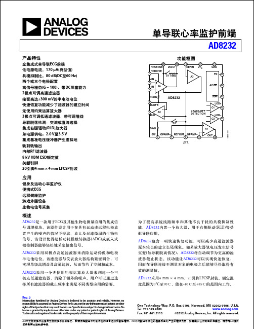
图1.
应用
健身及运动心率监护仪 便携式ECG 远程健康监护 游戏外围设备 生物电信号采集
概述
AD8232是一款用于ECG及其他生物电测量应用的集成信 号调理模块。该器件设计用于在具有运动或远程电极放 置产生的噪声的情况下提取、放大及过滤微弱的生物电 信号。该设计使得超低功耗模数转换器(ADC)或嵌入式 微控制器能够轻松地采集输出信号。 AD8232采用双极点高通滤波器来消除运动伪像和电极 半电池电位。该滤波器与仪表放大器结构紧密耦合,可 实现单级高增益及高通滤波,从而节约了空间和成本。 AD8232采用一个无使用约束运算放大器来创建一个三 极点低通滤波器,消除了额外的噪声。用户可以通过选 择所有滤波器的截止频率来满足不同类型应用的需要。
Rev. 0
为了提高系统线路频率和其他不良干扰的共模抑制性 能,AD8232内置一个放大器,用于右侧驱动(RLD)等受 驱导联应用。 AD8232包含一项快速恢复功能,可以减少高通滤波器 原本较长的建立长尾现象。如果放大器轨电压发生信号 突变(如导联脱离情况),AD8232将自动调节为更高的滤 波器截止状态。该功能让AD8232可以实现快速恢复, 因而在导联连接至测量对象的电极之后能够尽快取得有 效的测量值。 AD8232采用4 mm × 4 mm、20引脚LFCSP封装。额定温 度范围为0°C至70℃,能在-40℃至+85℃的范围内工作。
CS8323S_ch_v1.0
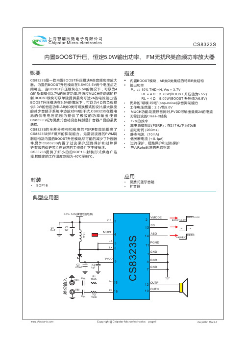
效率输出晶体管的开关工作方式决定了D 类放大器的高效率。
在D类放大器中,输出晶体管就像是一个电流调整开关,切换过程中消耗的额外功率基本可以忽略不计。
输出级相关的功率损耗主要是由MOSFET 导通电阻与电源电流产生的I R 。
升压启动后CS8323S 的效率可达72%。
CS8323S 无需滤波器的PWM 调制结构减少了外部元件数目,PCB 面积和系统成本,并且简化了设计。
芯片内置了过流保护,过热保护和欠压保护功能,这些功能保证了芯片在异常的工作条件下关断芯片,有效地保护了芯片不被损坏,当异常条件消除后,C S8323S 有自恢复功能可以让芯片重新工作。
2无需滤波器CS8323S 采用无需滤波器的PWM 调制方式,省去了传统D 类放大器的LC 滤波器,提高了效率,为便携式设备的音频子系统提供了一个更小面积,更低成本的实现方案。
Pop & Click 抑制CS8323S 内置专有的时序控制电路,实现全面的Pop & Click 抑制,可以有效地消除系统在上电,下点,Wake up 和Shutdown 操作时可能会出现的瞬态噪声。
保护电路CS8323S 在应用的过程中,当芯片发生输出管脚和电源或地短路,或者输出之间的短路故障时,过流保护电路会关断芯片以防止芯片被损坏。
短路故障消除后,CS8323S 自动恢复工作。
当芯片温度过高时,芯片也会被关断。
温度下降后,CS8323S 可以继续正常工作。
当电源电压过低CS 8323S EMI SpectrumA M P L I T U D E (dB u V /m )FREQUENCY(MHZ) Oct,2012Rev.1.0Oct,2012Rev.1.0。
汤姆逊 摄像机基站 控制面板 OCP 400 中文操作手册
Für diese Unterlage behalten wir uns alle Rechte vor (Gemäß DIN 34). Technische Änderungen im Zuge der Weiterentwicklung vorbehalten.
未经明确授权,严禁复制本文档、将 本文档转给他人、使用或传播本文中 的内容。违者必须赔偿损失。如果授 予专利或者实用模型或设计,我们保 留所有权利。在未来发展过程中有责 任进行技术改造。
摄像机设置 .............................................................. 12
摄像机调整 .............................................................. 14 调整白平衡 ............................................................... 14 光圈控制 .................................................................. 14 调整摄像机视频参数 ................................................ 14
用户指南
OCP 400
操作控制面板
3922 496 49931
版本 02
符合性声明
我们,Thomson Broadcast Solutions B.V., Kapittelweg 10, 4827 HG Breda, The Netherlands(荷兰),声明本 产品符合下列标准,并对此负责:
EN60065:安全性 EN55103-1:EMC(辐射) EN55103-2:EMC(抗扰度)
智浦欣微2015产品选型手册

CS8633D QFN8*8- 6.5V-18.5 4X15W 四通道(支 Po@10%THD+N,VDD=12.5V
家庭音箱
64L
V(DC 适配 持 BTL)
RL=8Ω 9.5W/CH,
2.0/2.1
器)
Po at 10% THD+N,VDD=14V
RL=4Ω,24W/CH
CS8655E ESOP16 6.5V-18.5 内 置 20 倍 增 益 , Po@10%THD+N,VDD=17V
( 双 节 锂 电 机驱动
Po@THD+N=10% VDD=8.5V
音箱
池)
RL=8Ω 5.0W(每通道)RL=4Ω9.0W
Po@THD+N=10% VDD=5V
RL=8Ω 1.8W RL=4Ω 3.2W
AB 类模式
Po@THD+N=10% VDD=8.5V
RL=8Ω 4W RL=4Ω 8W
Po@THD+N=10% VDD=5V
家庭音箱系统,
V(DC 适配 2X18W 立体声
RL=8Ω 2X18W,
LCD TV
器)
Po@10%THD+N,VDD=10V
RL=4Ω,2X10W
AB/D 可转换类
Part NO
CS8139S
封装
SOP8
工作电压
简介
功率
适用产品
2.5V-5.5V 5.0W,单声道,单 输出功率(D 类工作模式):
器)
Po@10%THD+N VDD=18V,
RL=8Ω 20W/CH(典型值),
Po@10%THD+N,VDD=24V
RL=8Ω 25W(典型值)
HIOKI 3286-20 钳式功率计 说明书
检查3286-20本体和附件
本体
3286-20 钳式功率计
附件
9245 便携盒
1
9635 电压测试线
1
手持带
1
LR6碱性干电池
1
操作手册
1
选件
9635-01 电压线
9636 RS-232C 电缆
9636-01 RS-232C 组件
9442 打印机
电话:010-51662244
-4-
网址:
电话:010-51662244
-8-
网址:
北京金三航科技发展有限公司
钳形电力谐波分析仪 3286-20 说明书
第一章 概述
1.1 产品概述
3286 钳形电力测试仪采用单片微处理器,可提供多种测试功能。在任何需要进行测试的单相或 三相回路测试点,使用 3286 可以测试电压、电流、功率、功率因数、相位角、有功或频率,并 能检测带电线路的相序。 使用选件 9636 RS232C 电缆,可将仪器连接到 9442 打印机(需另购),DATA OUTPUT(数据输出) 功能可将数据输出到打印机。
一次更新设置。(请参考2.10测量条件保存功能)
请求 我们已经努力使本手册尽量完善,但很可能仍有某些阐述不清或错误的部分,希望您能通
过我们的代理商或直接转告给我们,在此先表示感谢。
货运点检
您收到仪器后,请首先检查确认仪器在运输过程中没有损坏。特别是检查一下附件、面板开关 和接口。 若有仪器损坏或无法正常操作现象发生,请联系您的经销商或日置公司。
电话:010-51662244
-6-
网址:
北京金三航科技发展有限公司
钳形电力谐波分析仪 3286-20 说明书
·为了避免短路和潜在的生命危险,决不能将钳口夹在对地额定电压超过 600V 的电路或裸线上。 ·钳口只能连接到断路器的次级,这样断路器才可以防止因短路而发生的意外事故;决不能连 接到断路器的初级,因为一但发生短路的意外事故将无法得到保护。 ·先将电压线连接到仪器,再给被测线路通电。遵守以下事项以避免电击和短路:
S-8327资料
元器件交易网ContentsFeatures (1)Applications (1)Block Diagram (1)Selection Guide (2)Pin Assignment (3)Absolute Maximum Ratings (3)Electrical Characteristics (4)Test Circuits (9)Operation (10)External parts selection for DC-DC converter (13)Standard Circuits (17)Precautions (19)Application Circuits (20)Dimensions (25)Markings (25)Taping (26)Temperature Characteristics (29)Voltage Characteristics (31)Ripple Characteristics (32)Transient Responses (33)Operation Start Voltage and Operation HoldingVoltage Characteristics for Output Current (35)Input Voltage Characteristics for Input Current (35)Reference Data (36)Frequently Asked Question s (45)Seiko Instruments Inc.1S-8323/8327 SeriesSMALL PACKAGE PWM CONTROL STEP-UP SWITCHING REGULATORThe S-8323/8327 Series is a CMOS PWM-control step-up switching regulator which mainly consists of a reference voltage source, anoscillation circuit, a power MOS FET (for S-8323 Series) , and an error amplifier. The new PWM control circuit automatically changes the duty ratio from 0% to 83% according to the current load, offering products of a wide range, high efficiency. A step-up switching regulator isconstructed by externally connecting only a coil, a capacitor and a diode to the S-8323 Series. This feature, along with its small package and low current consumption, makes the S-8323 Series ideal for the power supply of portable equipment. For applications requiring a high output current, products used with an external transistor (S-8327 Series) are also available.FeaturesApplicationsLow voltage operation: 0.9 V (I OUT = 1mA)Power supplies for portable equipment such as Low current consumption :pagers, handy calculators, and remote controllers During operation: 17.2µA (typ.)Constant voltage power supplies for cameras,(V OUT = 3 V, 50 kHz)video equipment, and communications equipment During shutdown : 0.5µA (max.)Power supply for microcomputersDuty ratio:Built-in PWM control circuitExternal parts:coil, diode, and capacitor only(a transistor is needed for the S-8327 Series.) Output voltage: accuracy of ±2.4% Soft start function: 6 msec (typ.) Shutdown functionExternal transistor type is available (S-8327 Series) SOT-23-5 small plastic package SOT-23-3 small plastic packageSOT-89-3 miniature power molded plastic package Step-down and voltage-inverting type are available.Block Diagram(1) S-8323 Series(2) S-8327 SeriesFigure 1 Block Diagram(ON / OFF)EXT(ON / OFF)V SSV OUTCONTPWM control circuit-+VREFV SSV OUTPWM control circuit-+VREFSoft start circuitSoft start circuitSMALL PACKAGE PWM CONTROL STEP-UP SWITCHING REGULATORS-8323/8327 Series2Seiko Instruments Inc.Selection Guide1. Product NameS -832 X X XX XX - XXX -T2Tape SpecificationProduct name (abbreviation)Package name (abbreviation)MA: SOT-23-3 (without shutdown function)MC: SOT-23-5 (with shutdown function, V DD /Vout separate product)UA: SOT-89-3 (without shutdown function)Output voltage x 10Product categoryA: Normal product, fosc=50 kHz (S-8323 only)B: Normal product, fosc=100 kHz (S-8327 only)C: For pagers, fosc=30 kHz (S-8323 only)D : V DD /Vout separate product, fosc=50 kHz (S-8323 only)E : V DD /Vout separate product, fosc=100 kHz (S-8327 only)Power transistor 3: Built-in switch.7: External transistor.2. Product listOutput voltage(V)S-8323AXXMCSeries S-8323AXXMASeries S-8323AXXUASeries S-8323CXXMASeries S-8323DXXMCSeries2.0 ————S-8323D20MC-EZA-T22.5S-8323A25MC-ELF-T2S-8323A25MA-ELF-T2S-8323A25UA-ELF-T2S-8323C25MA-ENF-T2 —2.7S-8323A27MC-ELH-T2S-8323A27MA-ELH-T2S-8323A27UA-ELH-T2S-8323C27MA-ENH-T2 —3.0S-8323A30MC-ELK-T2S-8323A30MA-ELK-T2S-8323A30UA-ELK-T2S-8323C30MA-ENK-T2S-8323D30MC-EZK-T23.3S-8323A33MC-ELN-T2S-8323A33MA-ELN-T2S-8323A33UA-ELN-T2 — —5.0S-8323A50MC-EME-T2S-8323A50MA-EME-T2S-8323A50UA-EME-T2—S-8323D50MC-E3E-T25.2S-8323A52MC-EMG-T2 — — — —Output voltage(V)S-8327BXXMCSeries S-8327BXXMASeries S-8327BXXUASeries S-8327EXXMCSeries2.0 ———S-8327E20MC-EVA-T22.5S-8327B25MC-ERF-T2S-8327B25MA-ERF-T2S-8327B25UA-ERF-T2 —2.7S-8327B27MC-ERH-T2S-8327B27MA-ERH-T2S-8327B27UA-ERH-T2—2.8S-8327B28MC-ERI-T2 ———3.0S-8327B30MC-ERK-T2S-8327B30MA-ERK-T2S-8327B30UA-ERK-T2 —3.3S-8327B33MC-ERN-T2S-8327B33MA-ERN-T2S-8327B33UA-ERN-T2—3.6S-8327B36MC-ERQ-T2 ———5.0S-8327B50MC-ESE-T2S-8327B50MA-ESE-T2S-8327B50UA-ESE-T2S-8327E50MC-EKE-T25.4S-8327B54MC-ESI-T2———Consult our sales person for products with an output voltage other than specified above.3. Function ListProduct Name Built In power transistor with external power transistor Switching frequency (kHz)shutdown function V DD /V OUTseparate type Package Application ReferencepageS-8323AXXMC Yes —50Yes —SOT-23-5With shutdown function —S-8323AXXMA Yes —50 — —SOT-23-3Without shutdown function —S-8323AXXUA Yes —50 — —SOT-89-3Without shutdown function —S-8323DXXMC Yes —50 —Yes SOT-23-5For variable output voltage by step-up DC/DC converter and step-down, inverted output DC/DC converter with an external resistorPage 16S-8323CXXMA Yes —30 — —SOT-23-3For pagers —S-8327BXXMC —Yes 100Yes —SOT-23-5For large load current with shutdown functionPages 15 and 16S-8327BXXMA —Yes 100 — —SOT-23-3For large load current without shutdown functionPages 15 and 16S-8327BXXUA —Yes 100 — —SOT-89-3For large load current without shutdown functionPages 15 and 16S-8327EXXMC —Yes 100 —Yes SOT-23-5For variable output voltage bystep-up DC/DC converter with anexternal resistorPage 16SMALL PACKAGE PWM CONTROL STEP-UP SWITCHING REGULATORS-8323/8327 SeriesSeiko Instruments Inc.3Pin AssignmentFigure 2 Absolute Maximum RatingsNote:A protect circuit for static electricity is built into this IC chip.However, prevent a charge of static electricity which exceeds the capacity of the protect circuit.Pin No.Pin nameFunctions1ON / OFF Shutdown pin “H”:normal operation(stepping up operation)“L”:stop stepping up (whole circuit stop)2V OUT Output voltage pin and powersupply pin3—N.C. (Non Connection)4V SS GND pinCONT External inductor connection pin (for S-8323 Series)EXT External transistor connection pin (for S-8327 Series)Pin No. Pin name Functions1V OUT Output voltage pin 2V DD Power supply pin3—N.C. (Non Connection)4V SS GND pinCONT External inductor connection pin (for S-8323 Series)EXTExternal transistor connection pin (for S-8327 Series)Pin No.Pin name Functions 1V SS GND pin 2V OUT Output voltage pin and powersupply pinCONT External inductor connectionpin (for S-8323 Series)EXT External transistor connectionpin (for S-8327 Series)ParameterSymbol Ratings Unit VOUT pin voltage V OUT 11V ON/OFF pin voltage ON/OFF V ss - 0.3 to 11V CONT pin voltage V CONT 11V CONT pin current I CONT 300mA EXT pin voltage V EXT V ss - 0.3 to V OUT +0.3V EXT pin current I EXT±50mA Power dissipation PDSOT-89-3500mWSOT-23-5, SOT-23-3150Operating temperature T OPR -40 to +85°C Storage temperatureT STG-40 to +125°C 231SOT-23-3Top view54321SOT-23-5Top view321SOT-89-3Top view5S-8323AXXMC, S-8327BXXMC SOT-23-55S-8323DXXMC, S-8327EXXMCSOT-23-5 S-8323AXXMA, S-8323AXXUA, S-8323CXXMA S-8327BXXMA, S-8327BXXUA SOT-23-3, SOT-89-33( Unless otherwise specified: Ta=25°C)SMALL PACKAGE PWM CONTROL STEP-UP SWITCHING REGULATORS-8323/8327 Series4Seiko Instruments Inc.Electrical Characteristics1-1.S-8323AXXMC(Unless otherwise specified: Ta=25°C)Parameter Symbol ConditionsMin.Typ.Max.Unit Test circuitS-8323A52MC4.0755.200 5.325S-8323A50MC 4.880 5.000 5.120Output voltage V OUTS-8323A33MC 3.221 3.300 3.379S-8323A30MC 2.928 3.000 3.072S-8323A27MC 2.635 2.700 2.765V 1S-8323A25MC2.440 2.500 2.560Input voltageV IN ——9Operation start voltage V ST1I OUT =1mA——0.9Oscillation start voltage V ST2No external parts, voltage applied to V OUT CONT pulled up to 5 V by 10k Ω——0.82Operation holding voltageV HLDI OUT =1mA, Measured by decreasing V IN voltage graduelly0.7——1S-8323A52MC —31.652.6S-8323A50MC—30.250.3Current consumption 1I SS1V OUT =output voltage ×0.95S-8323A33MC—19.131.8S-8323A30MC —17.228.7S-8323A27MC —15.525.9S-8323A25MC —14.323.9S-8323A52MC — 3.5 6.9µA 2S-8323A50MC— 3.5 6.9Current consumption 2I SS2V OUT =output voltage+0.5S-8323A33MC— 3.3 6.5S-8323A30MC — 3.2 6.4S-8323A27MC — 3.2 6.4S-8323A25MC— 3.2 6.3Current consumption during shutdownI SSSshutdown pin=0V——0.5S-8323A52MC 114182—S-8323A50MC 114182—Switching current I SW VCONT=0.4V S-8323A33MC 78125—mA —S-8323A30MC 78125—S-8323A27MC 6198—S-8323A25MC6198—Switchin transistor leak currentI SWQ V OUT = VCONT=10V—— 1.0µA —Line regulation ∆V OUT1V IN =output voltage ×0.4 to ×0.6—3060mVLoad regulation ∆V OUT2I OUT =10µA to I OUT (below) ×1.25—3060S-8323A52MC —±0.26—Output voltage S-8323A50MC —±0.25—1temperature ∆V OUT /∆Ta Ta=-40°C to +85°CS-8323A33MC —±0.17—mV/°CcoefficientS-8323A30MC —±0.15—S-8323A27MC —±0.14—S-8323A25MC—±0.13—Oscillation frequency fosc V OUT =output voltage ×0.95Measured waveform at CONT pin 42.55057.5kHz Max. duty ratio MaxDuty V OUT =output voltage ×0.95Measured waveform at CONT pin 758390%Shutdown pin VSH V OUT =output voltage ×0.95Measured the oscillation at CONT pin 0.75——2Input voltage (ON/OFF type)VSL1V OUT =output voltage ×0.95WhenV OUT ≥1.5V——0.3VVSL2Judged the stop of oscillation at CONT pin When V OUT <1.5V——0.2Soft start time T SS3.0 6.012.0ms—S-8323A52MC—87—S-8323A50MC —87—Efficiency EFFI S-8323A33MC —83—%1S-8323A30MC —83—S-8323A27MC —79—S-8323A25MC—79—External parts used:- Coil:CD54 (100µH) of Sumida Electric Co., Ltd.- Diode:MA720 (Schottky type) of Matsushita Electronic Components Co., Ltd.- Capacitor:F93 (16V, 22µF, tantalum type) of Nichicon Corporation)Applied V IN =output voltage ×0.6, applied, I OUT =output voltage/250ΩThe shutdown pin is connected to V OUT pin.Note 1:The output voltage specified above is the typical value.SMALL PACKAGE PWM CONTROL STEP-UP SWITCHING REGULATORS-8323/8327 SeriesSeiko Instruments Inc.51-2.S-8323AXXMA, S-8323AXXUA, S-8323DXXMC(Unless otherwise specified: Ta=25°C)Parameter Symbol ConditionsMin.Typ.Max.Unit Test circuitS-8323X50XX4.8805.000 5.120S-8323X33XX 3.221 3.300 3.379Output voltage -V OUTS-8323X30XX 2.928 3.000 3.072S-8323X27XX 2.635 2.700 2.765V 1S-8323X25XX 2.440 2.500 2.560S-8323X20XX1.9522.000 2.048Input voltageV IN ——9Operation start voltage V ST1I OUT =1mA——0.9Oscillation start voltage V ST2No external parts, voltage applied to V OUT CONT pulled up to 5 V by 10k Ω——0.82Operation holding voltageV HLDI OUT =1mA, Measured by decreasing V IN voltage gradually.0.7——1S-8323X50XX —30.250.3S-8323X33XX—19.131.8Current consumption 1I SS1V OUT =output voltage ×0.95S-8323X30XX—17.228.7S-8323X27XX —15.525.9S-8323X25XX —14.323.9S-8323X20XX —11.619.4µA 2S-8323X50XX — 3.5 6.9S-8323X33XX— 3.3 6.5Current consumption 2I SS2V OUT =output voltage+0.5S-8323X30XX— 3.2 6.4S-8323X27XX — 3.2 6.4S-8323X25XX — 3.2 6.3S-8323X20XX — 3.1 6.2S-8323X50XX 114182—S-8323X33XX78125—Switching current I SW VCONT=0.4V S-8323X30XX78125—mAS-8323X27XX 6198—S-8323X25XX 6198——S-8323X20XX4571—Switchin transistor leak currentI SWQ V OUT = VCONT=9V—— 1.0µA Line regulation ∆V OUT1V IN = output voltage ×0.4 to ×0.6—3060mVLoad regulation ∆V OUT2I OUT =10µA to I OUT (below) ×1.25—3060S-8323X50XX —±0.25—Output voltage S-8323X33XX —±0.17—temperature ∆V OUT /∆Ta Ta=-40°C to +85°C S-8323X30XX —±0.15—mV/°C 1coefficientS-8323X27XX —±0.14—S-8323X25XX —±0.13—S-8323X20XX—±0.10—Oscillation frequency fosc V OUT =output voltage ×0.95Measured waveform at CONT pin 42.55057.5kHz2Max.duty ratio MaxDuty V OUT =output voltage ×0.95Measured waveform at CONT pin758390%Soft start timeT SS3.0 6.012.0ms—S-8323X50XX —87—S-8323X33XX —83—Efficiency EFFI S-8323X30XX —83—%2S-8323X27XX —79—S-8323X25XX —79—S-8323X20XX—75—External parts used:- Coil:CD54 (100µH) of Sumida Electric Co., Ltd.- Diode:MA720 (Schottky type) of Matsushita Electronic Components Co., Ltd.- Capacitor:F93 (16V, 22µF, tantalum type) of Nichicon Corporation)Applied V IN =output voltage ×0.6, I OUT =output voltage/250ΩThe V DD pin is connected to V OUT pin for V DD /V OUT separate product.Note 1:The output voltage specified above is the typical value.Note 2:V DD /V OUT Separate products:Boot operation is performed from V DD =0.8V.However, 2.0 V or more for V DD is recommended to stabilize the output voltage and oscilation frequency.SMALL PACKAGE PWM CONTROL STEP-UP SWITCHING REGULATORS-8323/8327 Series6Seiko Instruments Inc.1-3.S-8323CXXMA(Unless otherwise specified: Ta=25°C)ParameterSymbolConditionsMin.Typ.Max.Unit Test circuitS-8323C30MA2.9283.000 3.072Output voltage V OUT S-8323C27MA 2.635 2.700 2.765S-8323C25MA2.440 2.500 2.560V 1Input voltageV IN ——9Operation start voltage V ST1I OUT =1mA——0.9Oscillation start voltage V ST2No external parts, voltage applied to V OUT CONT pulled up to 5 V by 10k Ω——0.82Operation holding voltage V HLD Measured by decreasing V IN voltage gradually.0.7——1S-8323C30MA—11.619.3Current consumption 1I SS1V OUT =output voltage ×0.95S-8323C27MA—10.517.5S-8323C25MA —9.816.3S-8323C30MA— 3.0 5.9µA 2Current consumption 2I SS2V OUT =output voltage+0.5S-8323C27MA— 2.9 5.8S-8323C25MA — 2.9 5.8S-8323C30MA78125—Switching current I SW VCONT=0.4V S-8323C27MA6198—mAS-8323C25MA6198——Switching transistor leak currentI SWQ V OUT = VCONT=9V—— 1.0µA Line regulation ∆V OUT1V IN = output voltage ×0.4 to ×0.6—3060mVLoad regulation ∆V OUT2I OUT =10µA to I OUT (below) ×1.25—3060Output voltage S-8323C30MA —±0.15—1temperature ∆V OUT /∆Ta Ta=-40°C to +85°CS-8323C27MA —±0.14—mV/°C coefficientS-8323C25MA—±0.13—Oscillation frequency fosc V OUT =output voltage ×0.95Measured waveform at CONT pin 253035kHz2Max. duty ratio MaxDuty V OUT =output voltage ×0.95Measured waveform at CONT pin758390%Soft start time T SS 3.0 6.012.0ms —S-8323C30MA —81—EfficiencyEFFIS-8323C27MA —77—%2S-8323C25MA—77—External parts used:-Coil:CD54 (100µH) of Sumida Electric Co., Ltd.-Diode:MA720 (Schottky type) of Matsushita Electronic Components Co., Ltd.-Capacitor:F93 (16V, 22µF, tantalum type) of Nichicon Corporation)Applied V IN =output voltage´0.6, I OUT =output voltage/250ΩNote 1: The output voltage specified above is the typical value of the output voltage.SMALL PACKAGE PWM CONTROL STEP-UP SWITCHING REGULATORS-8323/8327 SeriesSeiko Instruments Inc.72-1.S-8327BXXMC(Unless otherwise specified: Ta=25°C)Parameter Symbol ConditionsMin.Typ.Max.Unit Test circuitS-8327B54MC5.270 5.400 5.530S-8327B50MC 4.880 5.000 5.120S-8327B36MC 3.514 3.600 3.686Output voltage V OUTS-8327B33MC 3.221 3.300 3.379S-8327B30MC 2.928 3.000 3.072S-8327B28MC 2.733 2.800 2.867V 3S-8327B27MC 2.635 2.700 2.765S-8327B25MC2.440 2.500 2.560Input voltageV IN ——9Operation start voltage V ST1I OUT =1mA——0.9Oscillation start voltage V ST2No external parts, voltage applied to V OUT——0.84Operation holding voltage V HLDI OUT =1mA, Measured by decreasing V IN voltage gradually.0.7——3S-8327B54MC —41.068.3S-8327B50MC —37.662.6S-8327B36MC—26.043.3Current consumption 1I SS1V OUT =output voltage ×0.95S-8327B33MC—23.739.5S-8327B30MC —21.435.7S-8327B28MC —20.033.3S-8327B27MC —19.232.0S-8327B25MC —17.829.7µA 4S-8327B54MC — 4.28.3S-8327B50MC — 4.28.3S-8327B36MC— 4.07.9Current consumption 2I SS2V OUT =output voltage+0.5S-8327B33MC— 4.07.9S-8327B30MC — 3.97.8S-8327B28MC — 3.97.8S-8327B27MC — 3.97.7S-8327B25MC— 3.97.7Current consumption while shutdownI SSSshutdown pin=0V——0.5S-8327B54MC -5.3-8.0—S-8327B50MC -5.3-8.0—S-8327B36MC -3.5-5.3—I EXTH VEXT=-0.4VS-8327B33MC -3.5-5.3—S-8327B30MC -3.5-5.3—S-8327B28MC -2.7-4.0—S-8327B27MC -2.7-4.0—EXT pin output current S-8327B25MC -2.7-4.0—mA —S-8327B54MC 10.716.0—S-8327B50MC 10.716.0—S-8327B36MC 7.010.5—I EXTL VEXT=0.4VS-8327B33MC 7.010.5—S-8327B30MC 7.010.5—S-8327B28MC 5.38.0—S-8327B27MC 5.38.0—S-8327B25MC 5.38.0—Line regulation ∆V OUT1V IN =output voltage ×0.4 to ×0.6—3060mVLoad regulation ∆V OUT2I OUT =10µA to I OUT (below) ×1.25—3060S-8327B54MC —±0.27—S-8327B50MC —±0.25—Output voltage S-8327B36MC —±0.18—3temperature ∆V OUT /∆Ta Ta=-40°C to +85°CS-8327B33MC —±0.17—mV/°CcoefficientS-8327B30MC —±0.15—S-8327B28MC —±0.14—S-8327B27MC —±0.14—S-8327B25MC—±0.13—Oscillation frequency fosc V OUT =output voltage ×0.95Measure waveform at EXT pin 85100115kHz Max. duty ratio MaxDuty V OUT =output voltage ×0.95Measure waveform at EXT pin 758390%Shutdown pin VSH V OUT =output voltage ×0.95Judged the oscillation at EXT pin 0.75——V4Input voltage (ON/OFF type)VSL1V OUT =output voltage ×0.95WhenV OUT ≥1.5V——0.3VSL2Judged the stop of oscillation at CONT pin When V OUT <1.5V——0.2Soft start timeT SS3.0 6.012.0ms—S-8327B54MC—88—S-8327B50MC —88—S-8327B36MC —84—Efficiency EFFI S-8327B33MC —84—%3S-8327B30MC —84—S-8327B28MC —80—S-8327B27MC —80—S-8327B25MC—80—External parts used:- Coil:CD54 (47µH) of Sumida Electric Co., Ltd.- Diode:MA720 (Schottky type) of Matsushita Electronic Components Co., Ltd.- Capacitor:F93 (16V, 47µF, tantalum type) of Nichicon Corporation)- Transistor: 2SD1628G of Sanyo Electronics - Base Resistance (Rb): 1. 0k Ω- Base Capacitor (Cb):2200 pFApplied V IN =output voltage ×0.6, I OUT =output voltage/50ΩThe shutdown pin is connected to V OUT pin.Note 1:The output voltage specified above is the typical value.SMALL PACKAGE PWM CONTROL STEP-UP SWITCHING REGULATORS-8323/8327 Series8Seiko Instruments Inc.2-2.S-8327BXXMA, S-8327BXXUA, S-8327EXXMC(Unless otherwise specified: Ta=25°C)Parameter Symbol ConditionsMin.Typ.Max.Unit Test circuitS-8327X50XX4.8805.000 5.120S-8327X33XX 3.221 3.300 3.379Output voltage V OUTS-8327X30XX 2.928 3.000 3.072S-8327X27XX 2.635 2.700 2.765V 3S-8327X25XX 2.440 2.500 2.560S-8327X20XX1.9522.000 2.048Input voltageV IN ——9Operation start voltage V ST1I OUT =1mA——0.9Oscillation start voltage V ST2No external parts, voltage applied to V OUT ——0.84Operation holding voltage V HLDI OUT =1mA, Measured by decreasing V IN voltage gradually B.0.7——3S-8327X50XX —37.662.6S-8327X33XX—23.739.5Current consumption 1I SS1V OUT =output voltage ×0.95S-8327X30XX—21.435.7S-8327X27XX —19.232.0S-8327X25XX —17.829.7S-8327X20XX —14.524.1µA 4S-8327X50XX — 4.28.3S-8327X33XX— 4.07.9Current consumption 2I SS2V OUT =output voltage+0.5S-8327X30XX— 3.97.8S-8327X27XX — 3.97.7S-8327X25XX — 3.97.7S-8327X20XX — 3.87.6S-8327X50XX -5.3-8.0—S-8327X33XX -3.5-5.3—I EXTHVCONT=-0.4VS-8327X30XX -3.5-5.3—S-8327X27XX -2.7-4.0—S-8327X25XX -2.7-4.0—EXT pin output current S-8327X20XX -1.9-2.9—mA —S-8327X50XX 10.716.0—S-8327X33XX 7.010.5—I EXTLVCONT=0.4VS-8327X30XX 7.010.5—S-8327X27XX 5.38.0—S-8327X25XX 5.38.0—S-8327X20XX3.8 5.7—Line regulation ∆V OUT1V IN =output voltage ×0.4 to ×0.6—3060mVLoad regulation ∆V OUT2I OUT =10µA to I OUT (below) ×1.25—3060S-8327X50XX —±0.25—Output voltage S-8327X33XX —±0.17—temperature ∆V OUT /∆Ta Ta=-40°C to +85°CS-8327X30XX —±0.15—mV/°C 3coefficientS-8327X27XX —±0.14—S-8327X25XX —±0.13—S-8327X20XX—±0.10—Oscillation frequency fosc V OUT =output voltage ×0.95Measured waveform at EXT pin 85100115kHz Max. duty ratio MaxDuty V OUT =output voltage ×0.95Measured waveform at EXT pin758390%4Soft start timeT SS3.0 6.012.0ms—S-8327X50XX —88—S-8327X33XX —84—Efficiency EFFI S-8327X30XX —84—%3S-8327X27XX —80—S-8327X25XX —80—S-8327X20XX—76—External parts used:- Coil:CD54 (47µH) of Sumida Electric Co., Ltd.- Diode:MA720 (Schottky type) of Matsushita Electronic Components Co., Ltd.- Capacitor:F93 (16V, 47µF, tantalum type) of Nichicon Corporation)- Transistor:2SD1628G of Sanyo Electronics - Base resistor (Rb): 1.0K Ω- Base capacitor (Cb):2200pF (ceramic)Applied V IN =output voltage ×0.6, I OUT =output voltage/50ΩThe V DD pin is connected to V OUT pin for V DD /V OUT separate product.Note 1:The output voltage specified above is the typical value.Note 2:V DD/V OUT Separate products:Boot operation is performed from V DD =0.8V.However, 2.0 V or more for V DD is recommended to stabilize the output voltage and oscilation frequency.SMALL PACKAGE PWM CONTROL STEP-UP SWITCHING REGULATORS-8323/8327 SeriesSeiko Instruments Inc.9Test Circuits1.Figure 3V SSV OUT CONTV-+-+(ON/OFF)2.3.4.V SSV OUT V-+-+(ON/OFF)Rb EXTV SS(ON/OFF)V OUTCONT 10k-+AV SS(ON/OFFV OUT-+AEXT CbOscilloscopeOscilloscopeOperation1.Step-Up DC/DC ConverterThe S-8323/8327 Series is a step-up switching regulator using a pulse width modulation method (PWM) and DC/DC converter and features a low current consumption.In conventional PFM DC/DC converters, pulses are skipped at low output load current, causing fluctuation in ripple frequency of the output voltage, with the result of increase in ripple voltage.The S-8323/8327 series operates with the PWM control which changes the pulse width duty from 0% to 83% according to the load current.The ripple voltage generated from switching can be removed easily through the filter because the switching frequency is constant.The built-in soft start circuit controls a rush current and overshoot of the output voltage when powering on or the ON/OFF terminal turns to “H” level.Shutdown pin:Stops or starts step-up operation.(Only for SOT-23-5 package products of A and B Series.)Turning the shutdown pin low stops operation of all the internal circuits and reduces current consumption significantly. DO NOT use the shutdown pin in floating state because it has a structure shown in Figure 4and is not pulled up or pulled down internally. DO NOT apply voltage of between 0.3 V and 0.75 V to the shutdown pin because applying such voltage increases the current consumption. If the shutdown pin is not used, connect it to V OUT pin.The shutdown pin doesn’t have hysteresis.Shutdown pinCR oscillationcircuit Output voltage “H”Operation Fixed “L”Stop~V IN *Figure 4ON/OFFV OUTV SS*Voltage obtained by extracting the voltage drop due to DC resistance of the inductor and the diode forward voltage from V IN.Figure 5+-+-OSC C OUTCONTM1V INLDiON/OFFV OUTThe following are basic equations [(1) through (7)] of the step-up switching regulator (see Figure 5.)Voltage at CONT pin the moment M1 is turned ON (current I L flowing through L is zero):The change in I L over time:Integration of the above equation (I L ):I L flows while M1 is ON (t ON ). The time of t ON is determined by the oscillation frequency of the OSC.The peak current (I PK ) after t ON :The energy stored in L is represented with 1/2 L (I PK )2.When M1 is turned OFF (t OFF ), the energy stored in L is transmitted through a diode to the output capacitor. Then reverse voltage (V L ) is generated.V L = (V OUT +V D ) - V IN (5)(V D : Diode forward voltage)The voltage at CONT pin rises only by the voltage corresponding to V OUT +V D .The change in the current flowing through the diode into V OUT during t OFF :Integration of the above equation is as follows:During t ON , the energy is stored in L and is not transmitted to V OUT . When receiving output current (I OUT ) from V OUT , the energy of the capacitor (C OUT ) is consumed. As a result, the pin voltage of C OUT is reduced, and goes to the lowest level after M1 is turned ON (t ON ). When M1 is turned OFF, the energy stored in L is transmitted through the diode to C OUT , and the voltage of C OUT rises drastically. V OUT is a time function that indicates the maximum value (ripple voltage: V P-P ) when the current flowing through the diode into V OUT and load current (I OUT ) match.Next, the ripple voltage is found out as follows:I OUT vs t 1 (time) from when M1 is turned OFF (after t ON ) to when V OUT reaches the maximum level:When M1 is turned ON (after t OFF ), IL=0 (when the energy of the inductor is completely transmitted). Based on equation (7),== (2)dI L dt V LL V IN - V S LI L =t (3)V IN - V SLV A =V S (1)(V S : Non-saturated voltage of M1)I PK =t ON (4)V IN - V S L== (6)dI L dtV LLV OUT +V D - V INLI L =I PK -t (7)V OUT +V D - V INLI OUT =I PK -t 1 (8)∴t 1= (I PK - I OUT ) (9)V OUT +V D - V INLV OUT +V D - V INL= (10)V OUT +V D - V INLI PKt OFFWhen substituting equation (10) for equation (9),Electric charge ∆Q1 which is charged in COUT during t1:When substituting equation (12) for equation (9):A rise in voltage (VP-P) due to ∆Q1:When taking into consideration I OUT to be consumed during t1 and ESR (Electric Series Resistance) of COUT, namely RESR:V P-P = = t1 + R ESR - (15)When substituting equation (11) for equation (15):Therefore to reduce the ripple voltage, it is important that the capacitor connected to the output pin has a large capacity and a small ESR.t 1=t OFF - t OFF (11)I PKI OUT∆Q 1= ∫ I l dt = I PK ∫ dt - ∫ tdt=I PK t 1 -=t 12 (12)t 10V OUT +V D - V INLV OUT +V D - V INL 210t 1t 1∆Q 1=I PK - (I PK - I OUT ) t 1 =t 1 (13)212I PK +I OUTV P-P == t1 (14)C OUT∆Q 1C OUT12I PK +I OUTC OUT ∆Q 1C OUT12I PK +I OUTC OUTI OUT t 12I PK +I OUTV P-P = + R ESR (16)2I PK(I PK - I OUT )2C OUTt OFF2I PK +I OUExternal parts selection for DC-DC converterThe relationship between majorcharacteristics of the step-up circuit and characteristics parameters of the external parts are shown in Figure 6.Figure 6 Relationship between major character stics of the step-up circuit and external partsfor large output current?for high efficiency?operation efficiencystand-by efficiencyfor small ripple voltagesmall inductancelarge inductancesmall DC resistance of inductorlarge output capacitancebuilt-in switchingtransistorexternal switching transistor(small ON resistance)small resistance of external resistor Rb when an external switchingtransistor is usedlarge resistance of external resistor Rb when an external switching transistor is used .。
MXT8234中文手册
1、特点z完美的立体声D/A转换系统:插值,D/A,模拟输出滤波z24位转换z96 dB动态范围z-88 dB的THD+Nz低时钟抖动灵敏度z单+5V电源供电z片上数字去加重功能z防冲击技术z功能上与CS4334兼容2、功能描述MXT8234系列是完美的立体声数模输出系统,在一个8脚封装中包含了插值、1位D/A转换和模拟输出滤波功能。
MXT8234支持主流的音频数据接口格式,并且不同器件的区别仅在于它们所支持的接口类型不同。
MXT8234是基于Delta-Sigma调制的转换器,其中的调制器输出用来控制一个超线性模拟低通滤波器的参考电压输入。
这种结构允许仅仅通过改变主时钟频率就可以在2kHz到100kHz范围内任意调节采样率。
MXT8234系列转换器均包含片上数字去加重功能。
片上去加重功能采用+5V电源供电,并且仅需要很少的支持电路。
这些特点对于置顶盒、DVD播放器、SVCD播放器和A/V接收机来说是非常理想的。
MXT8234功能框图3、特点和参数(在指定的工作条件下,所有的最小/最大值是有保证的。
典型性能指标是在理论工作电压和T A=25℃的条件下测试得到的。
)z指定工作条件(AGND=0V;所有电压都是相对于地的。
)参数 符号 最小 理论 最大 单位直流电源 VA 4.75 5.0 5.5 V工作环境温度(已加电) -KS -BS/-DS T A-10 - +70-40 - +85℃℃z极限工作条件(AGND=0V;所有电压都是相对于地的。
)参数 符号 最小 最大 单位 直流电源 VA -0.3 6.0 V 输入电流(除电源外) I in- ±10 mA 数字输入电压 V IND-0.3 VA+0.4 V 工作环境温度(已加电) T A-55 125 ℃ 存储温度 T stg-65 150 ℃● 模拟参数(满量程输出正弦波,997Hz;测试负载,RL=10kΩ,CL=10pF(见图1)。
SZ06 系列导轨无线采集设备用户使用手册说明书
SZ06系列导轨无线采集设备用户使用手册V1.0上海顺舟智能科技股份有限公司更新日期:2017-07-13文档修订记录版本 变化状态 日期 作者V1.0 更新文档 2017-07-13 SHUNCOM目录一、产品概述 (4)1.1 性能特点 (4)1.2 规格型号 (4)1.3 技术参数 (5)二、产品外观及接口 (6)2.1 产品外观尺寸 (7)2.2 接口及指示灯说明 (8)三、产品设置指南 (9)3.1 ZigBee无线参数设置 (9)3.2 WIFI无线参数设置 (12)3.3 GPRS无线参数设置 (15)3.4 采集参数设置 (17)3.5 参数说明 (18)四、数据格式说明 (19)4.1查询指令 (19)4.2设置指令 (21)4.3 IO控制指令 (22)4.4 保存参数指令 (23)4.5 数据计算 (23)五、通信调试 (23)5.1 ZigBee无线调试 (23)5.2 WIFI无线调试 (24)5.3 GPRS无线调试 (25)六、联系方式 (26)一、产品概述1.1、性能特点:性能特点产品主要功能采集模拟量、高低电平采集、温度采集高低电平输出,模拟量输出支持有线通信 RS485接口可用来透传数据或将采集的IO数据有线上传无线功能强大可选ZigBee、WiFi、GPRS采集方式灵活 支持定时主动上报或上位机查询功能灵活组合高低电平输入,高低电平输出,4-20MA输入,0-5V输入,温度采集等功能可以任意2种组合工业设计产品 工业环境应用设备,可在复杂的环境下使用1.2、规格型号:规格型号SZ06-XXX-XX-X -X产品系列无线技术IO功能IO数量 壳体类型SZ06-ZigBee-WiFi-GPRS00(高低电平采集)1-8路-D(导轨式壳体) 04(高低电平输出)05(4-20MA采集)06(4-20MA输出)07(0-10V电压采集)08(0-10V电压输出)12(PT100文档采集) 1-2路3C(高低电平采集控制)1-8路3D(高低电平控制输出)3E(4-20MA采集控制)3F(4-20MA控制输出)40(0-10V采集控制)41(0-10V控制输出)型号举例描述:规格型号无线技术 IO 功能壳体SZ06- ZigBee-(04-4-05-4)-DZigBee4路高低电平输出4路4-20MA 采集铝合金外壳1.3、技术参数:技术参数无线频率ZIGBEE/WIFI:2400-2485M 2.4G ISM 免费频段GPRS:850/900/1800/1900 MHz串口速率 波特率1200-115200可设置 输入电压 DC 5-24V尺寸 89.66mm*79.60mm*54.50mm 接口类型 RS485,IO设备天线 胶棒天线、吸盘天线等选配 工作温度 -40℃~+80℃ 工作湿度 10%~90%不结露 数据协议 MODBUS RTU 协议 数据上报支持主动上报及指令查询IO 功能高低电平采集、开关量采集、高低电平输出、4-20MA 采集、0-10V 采集、4-20MA 输出、0-10V 输出、PT100采集特殊说明壳体不密封,如需防水等特殊处理请与销售沟通二、产品外观及接口2.1 产品外观尺寸89.66mm*79.60mm*54.50mm2.2 接口及指示灯说明设备上端指示灯及接口说明:指示灯工作状态配置时状态PWR灯通电后常亮常亮ALM灯不亮1S/次闪烁NET灯组网成功后常亮(网络内需有中心节点)1S/次闪烁RUN灯1S/次闪烁1S/次闪烁侧面接口说明:1)SZ02-232/485无线数传设备接口说明Vin G G Vo A+ B- G RX TX G供电5-24V 电源地 电源地 输出5V485+ 485- 信号地 接用户232TX接用户232RX信号地CFGVin G G Vo A+ B- G RX TX G三、产品设置指南3.1 Zigbee无线参数设置1、硬件连接:SZ06的RS485接口通过USB转485转换器接电脑2、打开串口调试工具:选择正确的COM口,然后点击 打开串口 按钮;串口号:请选择正确的模块所对应的串口号。
CS5460A中文数据手册
DS284PP4
1
CS5460A
Байду номын сангаас目录
1.特性与规格说明..................................................................................................................................... 4 模拟特性 .............................................................................................................................................. 5 模拟特性(续) ................................................................................................................................... 6 5V 数字特性........................................................................................................................................ 7 3.3V 数字特性..................................................................................................................................... 7 绝对最大额定值 ................................................................................................................................... 8 开关特性 .............................................................................................................................................. 9