
charge trap NAND flash
Charge-Trap NAND Flash MemoryCharge Trap NAND Flash Memory Souvik Mahapatra pE E Dept, IIT Bombay, IndiaC t ib ti S d C P Si h S G t K hitij A l k Contributions:Sandya C, Pawan Singh, Suyog Gupta, Kshitij Auluck, Piyush Dak, Sandeep Kasliwal, Udayan Ganguly, Dipankar Saha, Gautam Mukhopadhyay, Juzer Vasi1Support:Applied Materials, Intel Corporation, SRC/GRCOutlineFG NAND Flash scaling challengesSiN based charge trap flash –material dependenceP/E simulation of SiN FlashMetal nanodot FlashScalability simulation of m-ND Flash2NAND Flash BackgroundBLDSLCGCD 15nm e l l sWL CD 15nmFG 50nm N o . o f c Figure: SamsungSSLTO 9nmL=35nmMemory stateSL•Electron transfer between substrate & FG define memory state (write &erase)state (write & erase)•FG surrounded by TO & CD acts as electron storage well (non-volatility, need 10yrs), though leak out occurs over time (retention loss )3•Repeated Write/Erase (10-100K needed) causes memory wear out (cycling endurance )NAND Flash Scaling•More memory, faster access, reduced cost •Guideline (ITRS roadmap):L=35nm (2009)CGCD 15nm Guideline (ITRS roadmap): L=35nm (2009), 28nm (2010/11), 22nm (2013/14)…SLC (1bit/ll)MLC (23bit /ll)f hi h TO 9nmFG 50nm •SLC (1bit/cell), MLC (2 or 3 bits/cell) for higher density, higher reliability issuesL=35nmScaling penalty:(1) Loss of CG –FG coupling (2)C ll t ll t lkSolution: Discrete trap-based charge storage(2) Cell to cell cross talk (3) Non-scaling of TO, FG and CD thickness CGCD,12nm CD thickness(4) Non-scaling of operating voltageTO, 6nmCD, 12nm SiN, 6nm 4(5) Higher reliability concernPlaner CTFDevices & test chip demonstrated (Samsung)•Memory windowMemory windowclose down with W/Ecycling•Data keeps leakingout(worse than FG!)out (worse than FG!)•Loss of memoryti5operationCTF reliability worse than FG, no product yetRetention IssueLateral or Vertical charge migration g gTrap depth of SiN is key to control charge migration 6Trap depth of SiN is key to control charge migration Solution –to cut SiN above STI (Samsung, 2007)NAND 3D Memoryp p y3D CTF proposed as a way to move forward below 20nm node: BiCs (Toshiba), TCAT (Samsung)7Motivationy pCTF reliability improvement needs:g p p g Understanding impact of device processing on material and electrical propertiesProper device design (structure, composition)Detailed electrical characterization & modeling –feedback for intelligent manufacturingg g8N+Si+ N+Si+N+Si+Summary•Comparison of SiN CompositionsParameterN+Si+Electron trap depth Deep Shallow Hole trap depth Hole trap depth Shallow Deep Hole trap density Very low High Split window operation Not possible Possible Endurance degradationHighLow17P/E Simulation of SiN Flash•Develop a Simulation framework capable of providing D l Si l ti f k bl f idi useful insight into the physics involved during Program /Erase (P/E) operations./Erase(P/E)operationsy p g•Accurately predicting P/E behavior of SANOS/SONOS memories•Simulation up to long time instants, large biasesSi l ti t l ti i t t l bi•For different gate stack dimensionsFor different gate stack dimensions•For different Nitride Compositionsp18Simulation Methodology•Set P/E bias•Compute Poisson throughoutCompute Poisson throughoutgate stack•Assume TO and CD as pureAssume TO and CD as puretunnel barriers, computetunneling currents in and outof SiN•Compute transport, continuityand SRH (trapping detrapping)and SRH(trapping detrapping)in SiNCo pute t apped c a ges,•Compute trapped charges,update Poisson•Continue till end of P/E time19Simulation Flow20Key Models IncorporatedTsu-Esaki tunneling formulationp pField dependent capture cross sectionPoole Frenkel detrapping from trapsTrap to band tunnelingT t b d t li21P/E: Stack Energy Band Diagrams22SANOS sample stack propertiesGate StackSiN Si2H6/N3flow ratio Dep.Temp RIGate StackDimensions(nm)type flow ratio(°C)TO SiN CD00052006N20.005650 2.0064615N20.005650 2.006661200052006N20.005650 2.0064612N00.01800 1.9874612N0ÆMore N rich SiN; N2ÆMore Si rich SiNDiff t t k di i d t h k b t23 Different stack dimensions used to check robustnessExtracted parameters (SiN dependence)Parameter N0N2ParameterN0N2Electron trap depth(eV) 1.8 1.63Hole Trap Depth (eV) 1.73 1.95()Electron trap density (1019cm -3) 3.33.9Hole Trap Density(1019cm -3) 1.62.6Electron σ const. , σ-0-122 5.7 5.7Hole σ const. , σ-0-10288(10cm )(10cm )Trap-band emissionf 13144Saturation electric field5V/)6.25 6.25freq. υ-tbt (1013s -1)E sat (105 V/cm)Values of carrier effective masses band gaps and30Values of carrier effective masses, band gaps and dielectric constants taken from published literatureSummary•New models for electric field dependent captureN d l f l t i fi ld d d t tcross section has been proposed which gives excellent agreement with experimental results excellent agreement with experimental results•The robustness of the simulator is verified across different stack thicknesses and different nitride compositions to accurately predict the P/E andISPP transients31Metal Nanodot (m-ND) Flash: Motivation•Floating Gate Cellpoly-Si storage gateNanodot Celldiscrete nanodots as –poly-Si storage gate –discrete nanodots as storage nodeC t l Di l t iControl GateFloating GateNanodots Control Dielectric SourceDrainCh le e e e e e eTunnel Dielectric SourceDrainCh le e e e eDefect inTunnel OxideComplete charge loss Only part of stored Channel Channel Charge storage in discrete nanodots increases Complete charge lossy pcharge is lost32immunity to tunnel oxide defectsm-ND Flash Process Flow SLDLWafer CleanTunnel Oxide 40ǺMetal Deposition AnnealILD deposition --ILD deposition Metal Deposition Si SiAnnealControl Oxide: 120Ǻ Al 2O 3Post Deposition Anneal Si l L (SL)D l L (DL)Post Deposition Anneal Metallization: 1000Ǻ PtSingle Layer (SL)Dual Layer (DL)33Pt Nanodot formation500o C700o C900o C5ÅInitialDeposited Thickness10ÅAnneal TemperatureOptimization of deposition and annealing processes results in large density(2)()(%)34(~4x1012cm -2),small size (~3nm)and large area coverage (~30%)Cross-Section TEMCDCDILDTO SiTODiscrete SL and DL nanodot formation clearly visible 35ySummary•Single and dual layer Pt metal Nanodot memorygate stacks demonstrated•Excellent memory window, cycling endurance(>10K ith6V i d)d t li(>10K with 6V window), pre-and post-cyclingretention•MLC capabilitiesMLC capabilities•No fundamental reliability show stopper for metaldots in gate stackdots in gate stack•Need feasibility demonstration in scaled (sub20nm node)cells20nm node) cells42Simulation of m-ND Flash•To demonstrate viability of m-ND cells in sub 20nm cells (impact of cell size no of dots area coverage (impact of cell size, no. of dots, area coverage,fluctuations, missing dots, dot to dot leakage…..)•Full 3D electrostatics and tunneling implementation S l L l f t ti l &l t i fi ld i t t k •Solve Laplace for potential & electric field in gate stack •Non-local tunneling implementation (Tsu-Esaki)forNon local tunneling implementation (Tsu Esaki) for charging of dots (substrate to dot, dot to gate, dot to dot)•Calculate charges in iterative mannerP t d t h i i l t d i i l t d i43•Port dot charges in equivalent device simulated using Sentaurus Device for VT calculationPotential, E-field, Tunnel current (2D cuts)44Charge Transients45Prediction….Area coverage, Channel length, No. density, Missing dots…46Summary•Full 3D electrostatics –tunneling framework to study m-ND Flash viability below 20nm node•Immunity to fluctuations (good)Immunity to fluctuations(good)Memory window reduction with L scaling (issue)•Memory window reduction with L scaling(issue)•Cells becomes edge critical (issue)47。
144层堆叠闪存投入使用 英特尔最新NAND SSD产品与技术解析

英特尔给出的金字塔多级存储结构 英特尔产品主要瞄准企业级用户,以高密度和高可靠性为特征。
英特尔在2021年上半年提供的数据中心产品方案,有3款新品。
英特尔2021年上半年面向消费者和客户端的产品
三星解释电荷陷阱技术,注意黄色的奶酪样的栅极。
一个典型的浮栅结构晶体管截面图
英特尔在存储产品上的发展历史
英特尔在不断提高3D NAND堆叠层数,提升存储密度。
英特尔的SSD产品在外形、NAND层数和每单元位数上做出了改进 英特尔3D NAND单元结构示意图
对比美光的置换栅极技术,
英特尔拥有更高的面密度。
高品质产品。
英特尔浮栅技术与替换栅极技术各自的优点 英特尔总结自家技术的优势 浮动栅极NAND能提供更高的数据保留率
采用144层堆叠QLC闪存,面向数据中心的英特尔D5-P5316固态硬盘。
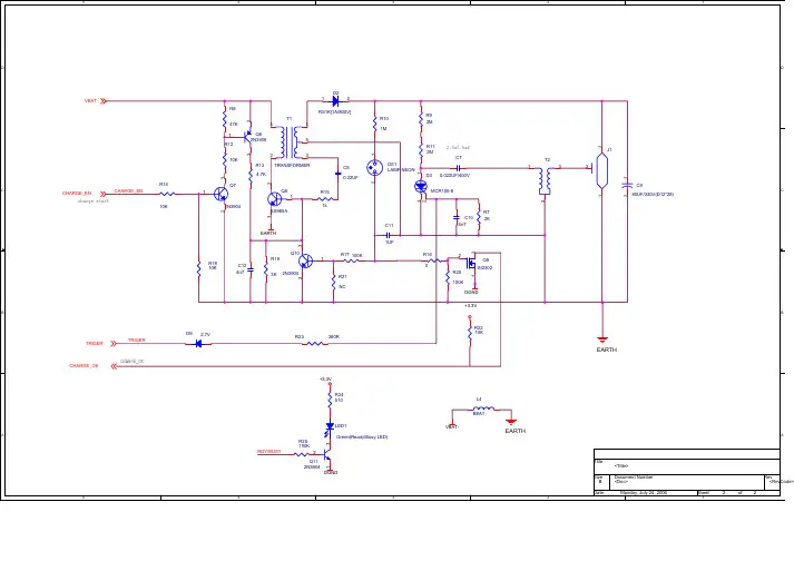
一个数码相机电路图
4
3
2
1
D
D
D2 VBAT R8 47K 1 R12 3 10K R13 4.7K 3 R14
C
1
2
RS1K[1A/800V] 2 T1 4 Q6 2N3906 1 5 2 3 TRANSFORMER C8 0.22UF 2 2 Q8 1 R15 1 R10 1M
R9 2M
R11 2M DS1 LAMP NEON
+3.3V
CARD_3.3V
V_DRAM R53 10K FMGPIO0 10K FMGPIO1 10K FMGPIO9
B
C6 10uF/6.3V GND R? 0
R54 R55
+3.3V
NAND_3.3V
C? 10uF/6.3V GND
Title SPCA531+CSTN+SOI268 PROJECT Size Date: Document Number NAND FLASH & SD Card Monday, February 27, 2006
U1 1 2 3 4 5 6 7 8 9 10 11 12 13 14 15 16 17 18 19 20 21 22 23 24 NC NC NC NC NC /SE R/nB /RE /CE NC NC VCC VSS NC NC CLE ALE /WE /WP NC NC NC NC NC NC NC NC NC IO7 IO6 IO5 IO4 NC NC NC VCC VSS NC NC NC IO3 IO2 IO1 IO0 NC NC NC NC 48 47 46 45 44 43 42 41 40 39 38 37 36 35 34 33 32 31 30 29 28 27 26 25
SK海力士宣布业内首款4D闪存:512Gb TLC、年末出样
SK 海力士宣布业内首款4D 闪存:512Gb TLC、年
末出样
正在美举办的Flash Memory Summit 首日已经结束,亮点颇多。
Keynote 环节,倒数第二个出场(排在我国的长江存储前)的是SK 海力士,它在NAND 市场的全球份额排名第五,DRAM 份额全球第二。
首先是3D NAND 的技术路线选择,SK 海力士称,CTF(Charge Trap Flash,电荷捕获型)比Floating Gate(浮栅型)存储单元面积更小、速度更快、更耐用(P/E 次数多)。
其实三星从2013 年的第一代V-NAND 3D 闪存就开始使用CTF 了,东芝/ 西数(闪迪)的BiCS 亦是如此。
当然,美光/Intel 还是坚持浮栅,不过这倒
无所谓,毕竟他们有更厉害的3D Xpoint(基于相变内存,还一说是ReRAM 磁阻式内存)。
接下来,SK 海力士宣布推出了全球首款4D 闪存。
从现场给出的技术演示来看,4D 闪存和此前长江存储的Xtacking 十分相似,只不过外围电路(PUC,Peri.Circuits)在存储单元下方,好处有三点,
一是芯片面积更小、二是处理工时缩短、三是成本降低。
AFND1G08U3-CKA规格书(K9F1G08)
• Copy-Back PROGRAM Operation - Fast Page copy without external buffering
z Status Register - Normal Status Register (Read/Program/Erase)
• Security features -OTP area, 16Kbytes(8 pages)
Initial Draft
June. 2012
Preliminary
Rev.01
Add new FBGA PKG dimension option (6.5x8.0mm 48B)
Nov. 2012
Rev. 02 Rev. 03
tRP(/RE Pulse Width) 12ns Æ 15ns
- VOH, VIL, VOL values control - Read Operation Figure modification - Write Protect figures added
PACKAGE DIMENSIONS
48-PIN LEAD/LEAD FREE PLASTIC THIN SMALL OUT-LINE PACKAGE TYPE(I)
Rev.03 Jan. 2013
Confidential
7
1G bit (128Mx8Bit)NAND FLASH
常用NAND Flash支持列表

Y
Y
第25脚 不能接
Y
32 Samsung 1GB MLC-2K K9G8G08U0A EC D3 14 A5 1CE 4b/512B 51nm 8Bit Y
Y
33 Samsung 1GB MLC-2K K9G8G08U0M EC D3 14 25 1CE 4b/512B 60nm 8Bit Y
Y
34 Samsung 1GB MLC-2K K9L8G08U0A EC D3 55 25 1CE 4b/512B 60nm 8bit Y
Y
2 Samsung 16GB MLC-4K K9MDG08U5M EC D7 55 B6 4CE 4b/512B 51nm 8bit Y
Y
3 Samsung 8GB MLC-8K K9LCG08U1M EC D7 94 72 2CE 24b/1KB 35nm 8bit Y
Y
4 Samsung 8GB MLC-4K K9HCG08U5M EC D3 14 A5 4CE 4b/512B 51nm 8Bit Y
Y
23 Samsung 2GB MLC-4K KLEAG8ZUMM EC D7 99 35 1CE
51nm 8Bit Y
Y
24 Samsung 2GB MLC-2K K9LAG08U0M EC D5 55 25 1CE 4b/512B 60nm 8Bit Y
Y
25 Samsung 2GB MLC-2K K9HAG08U1M EC D3 55 25 2CE 4b/512B 90nm 8Bit Y
Flash Support List
序号
Vendor 品牌
Capaci ty 容
量
Type 类 型
Flash存储芯片工作原理

Flash存储芯片工作原理引言概述:Flash存储芯片是一种常见的非易失性存储设备,广泛应用于各种电子设备中。
本文将详细介绍Flash存储芯片的工作原理,包括电荷存储原理、擦除和编程操作、读取操作、写入操作以及存储密度的提升。
正文内容:1. 电荷存储原理1.1 电荷存储单元:Flash存储芯片中的基本单元是电荷存储单元,每一个单元可以存储一个或者多个位的信息。
1.2 浮栅结构:每一个电荷存储单元都包含一个浮栅结构,浮栅上的电荷表示存储的信息。
当电荷存在时,代表存储的是“1”;当电荷不存在时,代表存储的是“0”。
2. 擦除和编程操作2.1 擦除操作:当需要将存储单元的值从“1”改写为“0”时,需要进行擦除操作。
擦除操作通过将浮栅上的电荷清除来实现。
2.2 编程操作:当需要将存储单元的值从“0”改写为“1”时,需要进行编程操作。
编程操作通过向浮栅注入电荷来实现。
3. 读取操作3.1 读取过程:读取操作是通过将电荷存储单元的信息转换为电压信号来实现的。
读取过程中,电荷存储单元的电荷会影响到读取电路中的电压,从而确定存储单元中存储的是“0”还是“1”。
3.2 读取精度:由于电荷存储单元中的电荷会逐渐漏失,因此在读取操作中需要进行补偿措施,以确保读取的准确性。
4. 写入操作4.1 写入过程:写入操作是通过向存储单元的浮栅注入或者清除电荷来实现的。
写入操作需要施加适当的电压和持续时间,以确保电荷的注入或者清除。
4.2 写入速度:写入操作的速度是衡量Flash存储芯片性能的重要指标之一。
随着技术的进步,写入速度逐渐提高。
5. 存储密度的提升5.1 单元尺寸缩小:随着创造工艺的进步,存储单元的尺寸逐渐缩小,从而提高了存储密度。
5.2 多层堆叠:为了进一步提高存储密度,Flash存储芯片采用了多层堆叠技术,将多个存储层叠加在一起。
5.3 三维堆叠:最新的技术发展使得Flash存储芯片可以实现三维堆叠,进一步提高了存储密度。
半导体trap原理
半导体trap原理
半导体中的trap(陷阱)是指能够俘获电子或空穴的晶体缺陷或物理中心。
这些陷阱能级是由于半导体中的杂质或晶格缺陷引入的。
当半导体处于热平衡状态时,这些能级上会有一定数量的热平衡电子。
当半导体受到外界激发,例如光照或电注入,会产生非平衡载流子,这些载流子可能会被陷阱能级俘获,从而改变半导体的电学性质。
陷阱能级分为电子陷阱和空穴陷阱。
如果陷阱能级上的电子数目增加,则该能级具有俘获非平衡电子的能力,称为电子陷阱。
反之,如果陷阱能级上的电子数目减少,则该能级具有俘获空穴的能力,称为空穴陷阱。
陷阱对半导体材料的载流子没有直接的贡献,但它们可以作为电子或空穴的复合中心,影响非平衡载流子的寿命。
当非平衡载流子落入陷阱后,基本上不能直接发生复合,而必须首先激发到导带或价带,然后才能通过复合中心而复合。
这个过程中,载流子从陷阱激发到导带或价带所需的平均时间比它们从导带或价带发生复合所需的平均时间长得多,因此陷阱的存在大大增加了从非平衡恢复到平衡态的弛豫时间。
陷阱在半导体器件中具有重要的应用,例如在金属-氧化物-半导体场效应晶体管(MOSFET)中,陷阱可以影响阈值电压和载流子迁移率等关键参数。
同时,陷阱也是半导体材料辐射损伤的主要原因之一,因为辐射会在半导体中产生大量的陷阱,从而影响器件的性能和可靠性。
96- 和 176 层 3d NAND 闪存的单事件影响响应说明书
Single-Event Effects Response of96-and176-Layer3D NAND Flash Memories Edward P.Wilcox,Member,IEEE,Matthew B.Joplin,Member,IEEE,Melanie D.Berg,Member,IEEEAbstract—Single-event effects testing(heavy-ion and proton)is presented for96-and176-layer commercially-available3D NAND flash memory,with emphasis on SEFI detection and recovery.Index Terms—Flash memory,proton,heavy ion,single-event upset,three-dimensional NAND,single-event functional interruptI.I NTRODUCTIONS TATE-OF-THE-ART3D NAND flash memories[1],[2] are characterized for single-event effects(SEE)response, including single-event upset(SEU),single-event latchup (SEL),and single-event functional interrupt(SEFI).With limited options for high-density radiation-hardened-by-design (RHBD)memories available,commercial parts are likely candidates for use in space,whether as-is or with significant aftermarket vendor screening and/or repackaging.These de-vices have well-known susceptibilities to multiple single-event effects phenomena[3]–[6].In this work,the SEE responses of three off-the-shelf devices are characterized and compared with heavy-ion and proton[7]irradiation,along with some exploration of the necessary mitigation steps to recover from complex error modes.II.D EVICES U NDER T ESTThe three commercial off-the-shelf(COTS)NAND flash devices tested are Micron96-and176-layer3D NAND flash, and SK Hynix176-layer3D NAND flash,further described in Table I.Throughout this document they are generally referred to based on the manufacturer and number of layers for convenience,e.g.,Micron96-layer flash.All are nominally triple-level cell(TLC)memories with the capability to operate in a classical single-level cell(SLC)mode for improved performance and endurance.Each device was prepared for heavy-ion testing by laser-chemical decapsulation to expose a single die as shown in Fig.1,Fig.2,and Fig.3.For proton testing,no decapsulation was performed.Submitted for publication on July14,2023.This work was funded by the NASA Electronic Parts and Packaging(NEPP)program.Authors acknowledge the support of Mike Wojtczak,Jeff Cassidy,and MEMKOR;the NASA GSFC Radiation Effects and Analysis Group(REAG);the Lawrence Berkeley National Laboratory;and Ethan Cascio of the Massachusetts General Hospital.E.P.Wilcox is with NASA Goddard Space Flight Center,Greenbelt,MD 20771USA(e-mail:*******************).M.B.Joplin is with NASA Goddard Space Flight Center,Greenbelt,MD 20771USA(e-mail:*************************).M.D.Berg is with SSAI,Inc.contracted by NASA Goddard Space Flight Center,Greenbelt,MD20771USA(e-mail:***********************).Fig.1.Decapsulated Micron96-layer flashmemoryFig.2.Decapsulated Micron176-layer flash memoryIII.T ESTING D ESCRIPTIONAll three devices were tested under heavy-ion irradiation at the Lawrence Berkeley National Laboratory’s(LBNL)88”Cyclotron[8];the Micron96-layer device in August of2022, and all three devices in November2022.Testing was per-formed with the16MeV/amu cyclotron tune using ions with incident linear energy transfer(LET)of approximately1.2to 56MeV·cm2/mg.All testing was performed in air.Testing at elevated temperature,where indicated,used resistive heating elements adhered to the printed circuit board;temperature was monitored by use of integrated on-chip temperature sensors within the NAND devices.High-energy proton testing was subsequently performed at the Massachusetts General Hospital’s Francis H.Burr Proton Therapy Center[9]in December2022.All three devices were characterized in varying degree to SEU and SEFI with125-and200-MeV protons.Some limited multi-die test results areTABLE ID EVICES U NDER T ESTPart Number MT29F8T08EWLGEM5MT29F8T08EWLKEM5H25G9TC18CX488ManufacturerMicronMicronSK Hynix3D NAND Technology 96Layers,SLC/TLC Floating Gate176Layers,SLC/TLC Replacement Gate176Layers,SLC/TLC Charge Trap(B27C)(B47T)(V7)Advertised Die Capacity512Gb TLC 512Gb TLC 512Gb TLC Total Capacity 8Tb TLC (16die)8Tb TLC (16die)512Gb TLC (1die)Lot Date Code IYG222PK22212TTested V oltageVCC:2.5V -3.3V VCC:2.5V -3.3V VCC:2.5V -3.3V VCCQ:1.25V VCCQ:1.25V VCCQ:1.25V Package132LBGA132LBGA152BGAFig.3.Decapsulated SK Hynix 176-layer flash memorypresented for the high-energy proton testing,but in general,testing was still based on a single die at a time.The airgap was 81cm and aperture size 3.5cm at 200MeV ,and the airgap 51cm and aperature size 2.5cm at 125MeV .A radiochromic film verified that the proton beam spot covered the flash memory device.Practical considerations of available beam time and test infrastructure generally preclude the complete testing of multi-terabit high-density memories.Instead,a representative sample of the array is characterized and assumptions made regarding the response of the entire device.A more thorough test is certainly appropriate when a specific application is targeted.In this work,the results sections indicate the size of memory tested,and test configuration,for each condition.In the case of heavy-ion testing at LBNL,it is only possible to test the top-most device in the stack due to ion range constraints.Heavy-ion SEFI testing included a fast (∼10ms)shutter mechanism in front of the device (Fig.4)to ensure that beam was only applied during specific operations [11],and that it could be immediately blocked from the device when a SEFI was detected.The fully-autonomous SEFI test detects anomalous device operation (or lack of any device response)and attempts recovery by RESET command,HARD RESET command,and finally by power cycle.RESET and HARD RESET are standard NAND flash commands documented by the manufacturer and communicated by the normal parallel databus.A power cycle physically pulls all device pins (both power and data)to 0V .Larger sample sizes are possible without the need to manually reconfigure the test between each event,and a more precise fluence-to-failure estimationFig.4.External shutter inserted in between facility and DUTis achieved by eliminating any manual response time.IV.H EAVY I ON R ESULTSA.Single-Event UpsetsAll SEU data were gathered with powered-off testing to isolate memory cell upsets from peripheral circuitry effects.The August 2022heavy ion data for the 96-layer Micron flash (Fig.7)represents four blocks (one per plane)totaling about 72MB of single-level cell (SLC)flash,and two blocks totaling about 108MB of triple-level cell (TLC)flash.The November heavy ion data (Fig.5)represents ten SLC blocks.It was observed initially that the SLC response was notice-ably better than expected at low LET compared to previously-published data for flash memories of generally-similar tech-nologies [5].After further investigation,the parts were tested again (Fig.5),but this time with adjustments made to the internal voltage threshold used to discriminate programmed cells (‘0’)from erased cells (‘1’)as provided in the man-ufacturer datasheet.Because NAND flash single-event upsets result in programmed (‘0’)cells turning into erased (‘1’)cells,it follows that adjusting the read offset setting towards theFig.5.Micron96-layer flash heavy-ion SEU responseerased state might increase the resistance to SEU,especially at lower LET where deposited charge is insufficient to fully shift a cell from0to1.See Fig.9for a generic illustration of this effect.Other tradeoffs(e.g.,long-term data retention) are possible.The black line in Fig.5is the original SLC data from Fig.7 with the default threshold voltages.The dashed line is a repeat of that test with zero offset explicitly set for confirmation of prior results.A clear trend of increased SEU hardness with lowered(i.e.,more negative)voltage threshold offset is present,as predicted by the effect of Fig.9.Similar test results are available for the176-layer Micron device in Fig.6.The Hynix device did not include a published mechanism to adjust the voltage threshold offsets and such testing was not performed in this study;a comparison of TLC and SLC SEU data is in Fig.8.B.Single-Event Functional InterruptsEach device was tested for susceptibility to single-event functional interrupts(SEFI),which are non-destructive(re-coverable)events caused by an upset in a critical element of control or peripheral circuitry that causes anomalous behavior. NAND flash SEFI are most easily grouped into those that cause a total loss of functionality requiring a power cycle, and those that cause malfunction within a portion of the memory array(e.g.,block-level SEFI that prevent successful READ,ERASE,or PROGRAM operations).The SEFI that completely disrupt functionality are detected in this test by frequent polling of the device with a READID command; this can be easily automated to collect statistically-significant volumes of events with accurate fluence-to-failure recorded. Additionally,the tester autonomously recovered from each of these SEFI and recorded whether a simple RESET orHARD Fig.6.Micron176-layer flash heavy-ion SEUresponseFig.7.Micron96-layer flash comparison of SLC and TLC modes RESET command was sufficient,or if the device required a power cycle to restore communications.Necessary and sufficient recovery steps for the Micron96-layer device are in Table II,for the Micron176-layer flash in Table III,those for the Hynix176-layer device are in Table IV, and breakdown of operational mode SEFI vulnerability in Table V.In Table V,a secondary shutter system was used to ensure the device was only exposed directly to the beam when the operational modes desired were active.Fig.8.SK Hynix 176-layer flash comparison of SLC and TLCmodesFig.9.Graphical diagram of the effect of varying LET on programmed flashcell threshold voltages.Green dashed lines are the programmed settings used to discriminate between programmed and erased SLC cells.SEFI testing of individual device operational modes was performed on all three memories.However,such testing is inherently time-consuming and not all combinations of device and operational mode were extensively characterized at all LET of interest;lack of data at any given LET does not imply a zero-error result.Data available are in Fig.10.Each device type is identified by marker shape,and each operational type during irradiation is indicated by color.Filled shapes indicateTABLE IISEFIRECOVERY STEPS NECESSARY FORM ICRON 96-LAYERDEVICELET (MeV·Fluence Count of READID SEFI resettable by -cm 2/mg)/cm 2RESET HARD RESET Pow.Cycle 18.02.01∗10610(77%)3(23%)0(0%)29.02.61∗10610(71%)1(7%)3(21%)56.08.58∗10689(77%)20(17%)6(5%)79.21.05∗107132(70%)40(21%)16(9%)Fig.10.Cross-section vs LET data for heavy-ion SEFI results in all three memories.TABLE IIISEFIRECOVERY STEPS NECESSARY FORM ICRON 176-LAYER DEVICELET Fluence Count of READID SEFI resettable by MeV·cm 2/mg/cm 2RESET HARD RESET Power Cycle 3.05.00∗1063008.02.01∗10620018.01.01∗10620029.01.00∗106700limiting cross-sections where no errors were observed during testing,and are computed as the inverse of the total tested fluence at that LET.SEFI operational testing was always performed with erase,program,read,and idle operations as typical of a data recorder-type application.In the case of an ERASE mode test,errors were detected in the erase or program stages by verifying the NAND status register flag was correctly set by the device indicating a successful operation after each erase or program command.Errors detected during readback were by means of an unrealistically-high error count at the block level.Following the erase-program-read-idle process,the device was reset and power cycled before restarting and re-opening the shutter.If a SEFI was observed during the active phase (e.g.,a failure to erase while under active irradiation)the beam was immediately blocked to minimize the probability of multiple events occurring during one cycle.In the case of a PROGRAM mode test,a single operational cycle was erase-program-read-idle-erase,such that the effects of a SEFI induced while programming could be evaluatedTABLE IVSEFIRECOVERY STEPS NECESSARY FORH YNIX 176-LAYERDEVICELETFluence Count of READID SEFI resettable by MeV·cm 2/mg/cm 2RESET HARD RESET Power Cycle 8.01.15∗10600029.01.0∗106010TABLE VSEFISUSCEPTIBILITY OFH YNIX 176-LAYER FLASH TO BLOCK -LEVEL ERASURE ,PROGRAMMING ,AND READBACK FAILURESLET Fluence Operational State While IrradiatingCount of block SEFI detected as failure to:MeV·cm 2/mg/cm 2ERASE PROGRAM READ 8.02.23∗105ERASE 39013858.02.23∗105PROGRAM 391818.02.23∗105READ 2503529.02.23∗105ERASE 4933829.02.23∗105PROGRAM 1676633129.02.23∗105READ200113144during all subsequent phases.Similarly,a READ mode testis constructed of erase-program-read-idle-erase-program,with only the read portion exposed to beam;subsequent SEFI observed during erase and program were fully evaluated prior to restarting the next test.These operational phases are similar to those described graphically and in more detail by [11].The total number of program-erase cycles did not approach the datasheet limits for these devices in either SLC or TLC mode.C.Single-Event LatchupTesting with 16MeV/amu Xe (incident LET 56.0MeV·cm 2/mg)revealed no single-event latchup (SEL)in any of the devices tested when irradiated at 85°C to a fluence of 1*107/cm 2at V CC of 3.3V .When irradiated at 45°angle (effective LET of 79.2MeV·cm 2/mg at die surface)no SEL was observed in the two Micron devices to a fluence of 1.05*107/cm 2.The Hynix 176-layer device had an anomalous high-current condition at this LET that reached power supply compliance and required a power cycle.This may be single-event latchup.Functionality was successfully recovered on-site,but further evaluation for latent damage has not been performed.The control circuitry for these devices is implemented under the flash memory stack (on the order of 10-20um below die surface).Beams used for this experiment had sufficient range to reach these circuits before the Bragg peak.However,precise estimation of tested LET requires construction analyses and will have the effect of raisingthe LET in the sensitive volume.V.P ROTON R ESULTSA.Single-Event UpsetsProton testing at the Massachusetts General Hospital’s Francis H.Burr Proton Therapy Center used 125-and 200-MeV proton irradiation to explore the proton sensitivity of the devices.Basic single-event upset test results are in Fig.11and represent test results with a 0x00repeating data pattern.To investigate any cumulative dose-related effects,one experiment included a series of exposures with intermediate measurement points to a total fluence of 1*1011p/cm 2.In Fig.12,four tests were performed without re-programming the memory.Then,a single test to the same fluence was performed for comparison.Proton testing also allowed the opportunity to explore the responses of individual die within the stacked part,rather than only a top-level die as in heavy-ion testing.In Fig.13,theFig.11.SEU data for all three devices with high-energy protons.Fig.12.Cumulative measurement of proton-induced upsets compared to a single measurement.125-and 200-MeV proton responses of all sixteen die are compared.The fluence for each energy was 1*1011p/cm 2.The actual physical order of the sixteen die is unknown.B.Single-Event Functional InterruptsSome 200-MeV proton SEFI test data is also available,though the overall sensitivity to SEFI with protons was rel-atively low.Testing was only performed with READID-style testing,in which the device ID is rapidly polled to verify basic functionality of the device.Results are in Table VI.BlockTABLE VISEFISUSCEPTIBILITY WITH200M E V PROTONS .Energy Device Total Fluence Observed Cross-sectionRecovery (MeV)(/cm 2)SEFI (cm 2)200SK Hynix 1761*101100N/A200Micron 964*101125.0*10−12Recovered with RESETMicron 176Not TestedFig.13.Proton-induced upsets in all sixteen die of the stacked device.SEFI events affecting memory integrity were not evaluated with protons.While the Micron 176layer device was not tested for SEFI with proton due to time constraints,it should be noted that this device had no READID SEFI (SEFI that resulted in loss of communications with the device)requiring more than a RESET command during heavy ion testing.VI.A CKNOWLEDGMENTSThe authors wish to thank additional colleagues at NASA GSFC for assistance with heavy ion testing and data analy-sis,including Michael Campola,Megan Casey,and Rebekah Austin,and wish to acknowledge Martha O’Bryan’s assistance with publication.R EFERENCES[1]K.Parat and A.Goda,“Scaling Trends in NAND Flash,”IEEE In-ternational Electron Devices Meeting ,San Francisco,CA,2018,pp.2.1.1-2.1.4.[2]L.Heineck and J.Liu,”3D NAND Flash Status and Trends,”2022IEEEInternational Memory Workshop (IMW),Dresden,Germany,2022,pp.1-4.[3]M.Bagatin et al.,”Single Event Effects in 3-D NAND Flash MemoryCells With Replacement Gate Technology,”in IEEE Transactions on Nuclear Science,vol.70,no.4,pp.308-313,April 2023[4]M.Bagatin et al.,”Effects of Heavy-Ion Irradiation on Vertical 3-DNAND Flash Memories,”in IEEE Transactions on Nuclear Science,vol.65,no.1,pp.318-325,Jan.2018.[5] E.P.Wilcox and M.J.Campola,”A TID and SEE Characterization ofMulti-Terabit COTS 3D NAND Flash,”2019IEEE Radiation Effects Data Workshop,San Antonio,TX,USA,2019,pp.238-244.[6] F.Irom,D.N.Nguyen and G.R.Allen,”Single Event Effect and TotalIonizing Dose Results of Highly Scaled Flash Memories,”2013IEEE Radiation Effects Data Workshop (REDW),San Francisco,CA,2013,pp.113-116.[7] D.Chen et al.,”Heavy Ion and Proton-Induced Single Event UpsetCharacteristics of a 3-D NAND Flash Memory,”in IEEE Transactions on Nuclear Science,vol.65,no.1,pp.19-26,Jan.2018.[8]M.K.Covo et al.,”88-Inch Cyclotron:The one-stop facility forelectronics radiation testing,”2017IEEE International Workshop on Metrology for AeroSpace (MetroAeroSpace),Padua,Italy,2017,pp.484-488.[9] E.W.Cascio,”A Five-Year Compendium of Proton Test Usage Patternsat the Francis H.Burr Proton Therapy Center,”2018IEEE Radiation Effects Data Workshop (REDW),Waikoloa,HI,USA,2018,pp.1-5.[10] F.Irom,D.N.Nguyen,G.R.Allen and S.A.Zajac,”Scaling Effectsin Highly Scaled Commercial Nonvolatile Flash Memories,”2012IEEE Radiation Effects Data Workshop,Tucson,AZ,2012,pp.103-108.[11] E.P.Wilcox,”Risk-Driven and Mitigation-Focused SEFI Testing ofNAND Flash Devices,”2022Single-Event Effects Symposium and Military &Aerospace Programmable Logic Device (SEEMAPLD)Workshop,La Jolla,CA,2022.。
存储器:3DNAND风暴来袭
存储器:3DNAND风暴来袭作者:莫大康来源:《中国电子报》2016年第59期自2013年8月三星率先宣布成功推出3D NAND之后,在技术上每年都会前进一步,由24层、32层、48层,到-今年的第四代64层。
有消息称2017年三星将可能推出80层3D NAND。
除技术进步之外,有分析师预测在2018年中期,全球NAND闪存市场在3D堆叠技术的影响下,价格有可能低到每Gb约3美分。
目前,中国正在下大力度推进存储产业的发展,3D NAND被认为是一个有利的突破口。
在此之际,有必要了解3D NADN的产业竞争形势。
全球3D NAND竞争形势加剧想要了解3D NAND,首先应当了解其关键制造工艺。
3D NAND的制造工艺十分复杂,主要包括高深宽比的沟开挖(High aspect ratio trenches)、在源与漏中不掺杂(No doping on source or drain)、完全平行的侧壁(Perfectlv parallel walls)、众多级的台阶(Tens of stairsteps)、在整个硅片面上均匀的淀积层(Uniform layeracross wafer)、一步光刻楼梯成形(sin-一e-Lithostairstep)、硬掩模刻蚀(Hardmask etching)、通孔工艺(Processing in-side of hole)、孔内壁淀积工艺(Deposi-tion on hole sides)、多晶硅沟道(Polvsih-con channels)、电荷俘获型存储(chargetrap storage)、各种不同材料的刻蚀(Etchthrough varyi‘ng materials)、淀积众多层材料(Deposition of tens of layers)等。
这些还只是主要关键部骤,可见其复杂性。
然而,2D NAND在进入1xnm节点之后,器件耐久性和数据保持特性持续退化,单元之间的耦合效应难以克服,很难解决集成度提高和成本控制的矛盾,进一步发展面临瓶颈。
先进半导体存储器3
Introduction to Advanced Semiconductor Memories (III) P. Zhou Fudan University 2008-9-181课程安排 第三讲(9.18)FLASH 1 第四讲(9.25)FLASH 2 第五讲(10.9)FLASH 3 第六讲(10.16)Materials Characterization 1 Presentation I (10.23) Presentation II (10.30) 第七讲(11.6)Materials Characterization 2 第八讲(11.13)PRAM&MRAM&FeRAM 第九讲(11.20)RRAM 第十讲(11.27)RRAM 第十一讲(12.4)RRAM Final Project I (12.11) Fianl Project II (12.18) 第十二讲(12.25)ReviewSchool of Microelectronics课程内容• 以DRAM为例:1School of MicroelectronicsSchool of MicroelectronicsSchool of MicroelectronicsBASIC PrincipleCharges are stored in the insulator of a MOSFET, the threshold voltage of the transistor can be modified to switch between two values. The data is read by applying a gate voltage with a value between the two possible threshold voltages. In one state, the transistor is conductive. In the other, the transistor is cut off. When no power, the charge remain stored in the gate insulator.School of MicroelectronicsThe storage of the chargeΔVTH = −Threshold voltage shiftQTεIdISchool of MicroelectronicsThe storage of charges can be realized in two ways:a.Based on a conducting or semi-conducting layer that is surrounded by a dielectric. Name: Floating gate deviceb.The charge is stored in discrete trappping center of an appropriate dielectric layer. Name: charge trapping device.School of MicroelectronicsProgramming MechanismsElectrical conduction through thin dielectric filma. b. Bulk limited e.g. Si3N4 Interface limited e.g. SiO2 The current is determined mainly by the electrode or the injection interface The current is determined mainly by the dielectric itself, e.g. Poole-Frenkel conductionSchool of MicroelectronicsCharge InjectionF-N TunnelingQuantum tunnelingEnhanced F-N Channel hot-electron injection (CHE) Source side injection SSISchool of MicroelectronicsF-N Tunneling32*3/2*exp[]8423c inj b inj bc E q m J E h m E E mqπφφ−===α此最简单形式忽略了镜像力导致的有效势垒降低与温度依赖。