OXT1000系列
朗宏氧化锆

氧化锆氧量分析氧化锆氧量分析仪仪用户手册用户手册 Version 10.07.29在使用本产品在使用本产品之前之前之前,,请务必先仔细阅读本用户手册请务必先仔细阅读本用户手册。
请务必妥善保管好本书请务必妥善保管好本书,,以便日后能随时查阅以便日后能随时查阅。
请在充分理确内容的基础上请在充分理确内容的基础上,,正确使用正确使用。
目 录1系统概述 (1)1.1测量原理 (1)1.2氧量分析系统的结构 (2)2 系统说明 (3)2.1 氧量探头 (3)2.2电子变送器 (4)2.3 专用电缆 (5)2.4 标定装置 (5)3 系统安装 (7)3.1 氧量探头的安装位置选择 (7)3.2 氧气探头的安装 (7)3.3 电子变送器的安装 (9)4 电子变送器的说明 (11)4.1 概述 (11)4.2 设备运行 (11)4.3 DIP 开关设置 (17)5 技术指标 (18)5.1 智能电子变送器特性 (18)5.2 探头特性 (18)6 维修 (19)6.1 保险丝的更换 (19)6.2 过滤器的清洗和更换 (19)6.3探头内芯的拆装 (20)6.4 锆电池的更换......................................................................................................................20 附录一附录一::系列氧量分析选型表...................................................................................22 附录二附录二::防磨保护套管选型表.. (23)附录三附录三::法兰孔位尺寸选型表.....................................................................................................24 附录四附录四::主要配件清单.. (25)24个月个月的的质量保证质量保证期期深圳市朗弘科技有限公司深圳市朗弘科技有限公司((LONHOT LONHOT))保证由它制造和销售的设备保证由它制造和销售的设备,,在设备正式投运后两年质保期内两年质保期内,,不会出现因工艺或材料造成的故障不会出现因工艺或材料造成的故障。
Keysight InfiniiVision 1000 X-Series 双通道和四通道传感器接收仪
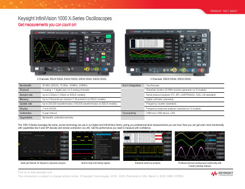
10:1 400 MHz extreme temperature passive probe
100:1 500 MHz 3.7 KV high voltage passive probe
Included standard
Standard passive probes (Two N2142A for EDUX1052A/G; Two N2140A for DSOX1202A/G; Four N2140A for DSOX1204A/G) Standard secure erase Interface language support GUI: English, Japanese, Simplified Chinese, Traditional Chinese, Korean, German, French, Spanish, Russian, Portuguese, Italian, Polish, Czech, Thai, and Turkish Built-in help language support for English, Japanese, Simplified Chinese, Traditional Chinese, Korean, German, French, Spanish, Russian, Portuguese, Italian, Polish, and Thai Localized Power cord Certificate of calibration
Bode plot feature for frequency response analysis
Built-in help and training signals
tektronix wp1000 数字处理波形显示器说明书

PROGRAM GALI
su 20
நோக்க
TP7A00K1TPROOCNESSO1 R ***
NE
olles CALARA w
WYXNXHO GKKE *****
E
A
Chop EN
a,ll formel |
3,1 gul aalatul
ROS
el TOY
VO
BE
++++
7A1BA AURER WALA A7704 ACQUISITION UNIT
3-1 3-1
1 3-1
1 3-1 3-3
3-5
1
ii
@
IPUU
WP1000 SERIES
.
PORUS
TESTED BY
love
2015
OSCILL7O7SC0O4PEABYSTEM
THERE 02704 DIEPLAY UNIT
DISPLAY SOURCE
DATA NAMOLINO TO
MEMORY LOGAVION
Manual Summary Table 1-1 shows the available manuals for this configuration . This Introduction Manual gives you a general description of the
WP1000 and a brief review of the manuals . The second section gives you some suggestions for cabling and assembling the WP1000 . The third section of this manual is a WP1000 Diagnostic Procedure .
660MW机组锅炉氧量测点安装位置对正确测量的影响分析

660MW机组锅炉氧量测点安装位置对正确测量的影响分析作者:胡晓亮来源:《科技资讯》2014年第33期摘要:锅炉炉膛出口氧量参数是锅炉运行中的重要参数。
不仅对锅炉效率有着重要的影响,而且还将引起其他运行参数的变化,进而影响机组的供电煤耗率。
大唐信阳发电有限责任公司自#3机组投产以来,空预器出口氧量一直显示偏小,机组停运期间通过对#3炉A1氧量计移位改造,解决了这一难题,由此说明氧量计安装位置对正确测量有着至关重要的影响。
为了验证改造后A1氧量计的准确性,进行了氧量测点安装位置对正确测量的影响分析试验,进而为火电厂优化氧量测量提供参考。
关键词:660MW 烟气含氧量氧量分析仪中图分类号:TM62 文献标识码:A 文章编号:1672-3791(2014)11(c)-0046-01大唐信阳发电有限责任公司#3锅炉系东方锅炉厂生产的型号为DG2000/26,15-Ⅱ2型超超临界煤粉锅炉。
针对#3炉出现氧量偏小的现象,大唐信阳发电有限责任公司在检修中,更换了A1氧量计的位置,为验证A1氧量计的准确性及移动后的位置是否合适,且寻找合适的烟道氧量代表点,对#3炉A1氧量计进行校核及氧量代表标定试验。
1 主要设备技术规范#3锅炉为东方锅炉股份有限公司生产的DG2000/26,15-II2型一次中间再热、超超临界参数的直流变压运行锅炉。
单炉膛、尾部双烟道结构、采用烟气挡板调节再热汽温、固态排渣、全钢构架、全悬吊结构、平衡通风、露天布置、前后墙对冲燃烧方式。
氧量计采用的是深圳朗弘科技有限公司OXT1000系列氧量计。
2 试验内容(1)#3机组450 MW负荷下,总风量2000 t/h时A1氧量计校核及氧量代表点标定试验;(2)#3机组530 MW负荷下,总风量2240 t/h时A1氧量计校核及氧量代表点标定试验;(3)#3机组640 MW负荷下,总风量2700 t/h时A1氧量计校核及氧量代表点标定试验。
3 测点布置与测量方法3.1 测点位置布置每块氧量计烟气取样管处都设计有标定专用旁路管道,使用此旁路管道首先校核A1氧量计。
XX1000中文资料

Mimix Broadband ’s single ended fed (no external balun required) 7.5-25.0/15.0-50.0 GHz GaAs MMIC doubler has a +15.0 dBm output drive and is an excellent LO doubler that can be used to drive fundamental mixer devices. It is also well suited to drive Mimix's XR1002 receiver device. This MMIC uses Mimix Broadband ’s 0.15 µm GaAs PHEMT device model technology, and is based upon electron beam lithography to ensure high repeatability anduniformity. The chip has surface passivation to protect and provide a rugged part with backside via holes and gold metallization to allow either a conductive epoxy or eutectic solder die attach process. This device is well suited for Millimeter-wavePoint-to-Point Radio, LMDS, SATCOM and VSAT applications.7.5-25.0/15.0-50.0 GHz GaAs MMIC Excellent Broadband Mixer DriverSingle Ended Fed Doubler with Distributed Buffer AmplifierExcellent LO Driver for Mimix Receivers +15 dBm Output Drive100% On-Wafer RF, DC and Output Power Testing 100% Visual Inspection to MIL-STD-883Method 2010FeaturesElectrical Characteristics (Ambient T emperature T = 25 o C)ParameterInput Frequency Range (fin)Output Frequency Range (fout)Input Return Loss (S11)Output Return Loss (S22)Harmonic Gain (fout)Fundamental Rejection (fin) Saturated Output Power (Psat)RF Input Power (RF Pin)Output Power at +0.0 dBm Pin (Pout)Drain Bias Voltage (Vd1,2)Gate Bias Voltage (Vg1)Gate Bias Voltage (Vg2)Supply Current (Id1,2) (Vd=5.0V, Vg1=-0.6V, Vg2=0.0V Typical)Source Voltage (Vss)Source Current (Iss)Units GHz GHz dB dB dB dBc dBm dBm dBm VDC VDC VDC mA VDC mA Min.7.515.0------10.0---1.2-1.2--5.525Typ.--TBD 12.01320+15-+13.0+5.0-0.60.0220-5.050Max.25.050.0-----+10.0-+5.5+0.1+0.1250-2.060Absolute Maximum RatingsSupply Voltage (Vd)Supply Voltage (Vss)Supply Current (Id)Supply Current (Iss)Gate Bias Voltage (Vg)Input Power (RF Pin)Storage Temperature (Tstg)Operating Temperature (Ta)Channel Temperature (Tch)+6.0 VDC -6.0 VDC 300 mA 60 mA +0.3 VDC +12.0 dBm -65 to +165 O C -55 to MTTF Table MTTF Table Chip Device Layout1(1) Channel temperature affects a device's MTTF. It is recommended to keep channel temperature as low as possible for maximum life.1April 2006 - Rev 10-Apr-06General DescriptionDoubler Measurements0458_4_sa mples: Po ut (2xFin) vs. Fin (GHz)Pin=0dBm, VD1=5V, VG1=-0.6V, VS S=-5V, VD2=5V ~150mA, VG2=open101214161820Fin (GHz)Pout(2xFin)0458_4_s amples: Pout (Fin) vs. F in (GHz)Pin=0dBm, VD1=5V, VG1=-0.6V, VS S=-5V, VD2=5V ~150mA, VG2=open-5101520810121416182022Fin (GHz)Pout(Fin)7.5-25.0/15.0-50.0 GHz GaAs MMICHarmonic Gain and Fundamental Rejection vs Output Freq.Pin = 0 dBm XX1000: Po ut (2xFin) an d Po ut (F in) v s. F in (GHz)Pin = -8 to +6 dBm810121416182022Fin (GHz)Pout(dBm)April 2006 - Rev 10-Apr-06Mechanical DrawingBypass Capacitors- See App Note [2] (Note: Engineering designator is 40DBL0458)Units: millimeters (inches) Bond pad dimensions are shown to center of bond pad. Thickness: 0.110 +/- 0.010 (0.0043 +/- 0.0004), Backside is ground, Bond Pad/Backside Metallization: GoldAll Bond Pads are 0.100 x 0.100 (0.004 x 0.004).Bond pad centers are approximately 0.109 (0.004) from the edge of the chip.Dicing tolerance: +/- 0.005 (+/- 0.0002). Approximate weight: 1.566 mg.Bond Pad #1 (RF In) Bond Pad #2 (Vd1)Bond Pad #3 (Vd2)Bond Pad #4 (RF Out)Bond Pad #5 (Vg2)Bond Pad #6 (Vss)Bond Pad #7 (Vg1)7.5-25.0/15.0-50.0 GHz GaAs MMICApril 2006 - Rev 10-Apr-061.620(0.064)0.2950.6950.196(0.035)(0.061)(0.019)(0.012)0.01234567Vd2Vg1App Note [1] Biasing - It is recommended to separately bias each doubler stage Vd1 through Vd2 at Vd(1,2)=5.0V with Id1=80mAand Id2=140mA and Vss=-5.0V with Iss=50mA. XX1000 provides good performance at reduced bias with Vss=-2.0V and Iss=25mA.Maximum output power is achieved with Vss=-5.0V and Iss=50mA. Separate biasing is recommended if the doubler is to be used at high levels of saturation, where gate rectification will alter the effective gate control voltage. It is also recommended to use active biasing to keep the currents constant as the RF power and temperature vary; this gives the most reproducible results. Depending on the supply voltage available and the power dissipation constraints, the bias circuit may be a single transistor or a low power operational amplifier, with a low value resistor in series with the drain supply used to sense the current. The gate of the pHEMT is controlled to maintain correct drain current and thus drain voltage. The typical gate voltages needed to do this are Vg1=-0.6V and Vg2=0.0V. Typically the gate is protected with Silicon diodes to limit the applied voltage. Also, make sure to sequence the applied voltage to ensure negative gate bias is available before applying the positive drain supply.App Note [2] Bias Arrangement -For Individual Stage Bias (Recommended for doubler applications) -- Each DC pad (Vd1, 2, Vss and Vg1, 2) needs to have DC bypass capacitance (~100-200 pF) as close to the device as possible. Additional DC bypass capacitance (~0.01 uF) is also recommended.MTTF T able s (TBD)These numbers were calculated based on accelerated life test information and thermal model analysis received from the fabricating foundry.Backplate Temperature 55 deg Celsius 75 deg Celsius 95 deg CelsiusChannel Temperature deg Celsius deg Celsius deg CelsiusFITs E+E+E+MTTF HoursE+E+E+Rth C/W C/W C/WBias Conditions: Vd1=Vd2=4.0V, Id1=40 mA, Id2=140 mA, Vss=-5.0V, Iss=50mA7.5-25.0/15.0-50.0 GHz GaAs MMICApril 2006 - Rev 10-Apr-06Device SchematicMimix Broadband MMIC-based 18.0-34.0 GHz Doubler/Receiver Block Diagram(Changing LO and IF frequencies as required allows design to operate as high as 34 GHz)T ypical ApplicationXR10027.5-25.0/15.0-50.0 GHz GaAs MMIC April 2006 - Rev 10-Apr-06Handling and Assembly InformationCAUTION! - Mimix Broadband MMIC Products contain gallium arsenide (GaAs) which can be hazardous to the human body and the environment. For safety, observe the following procedures:Do not ingest.Do not alter the form of this product into a gas, powder, or liquid through burning, crushing, or chemical processing as these by-products are dangerous to the human body if inhaled, ingested, or swallowed.Observe government laws and company regulations when discarding this product. This product must be discarded in accordance with methods specified by applicable hazardous waste procedures.Life Support Policy - Mimix Broadband's products are not authorized for use as critical components in life support devices or systems without the express written approval of the President and General Counsel of MimixBroadband. As used herein: (1) Life support devices or systems are devices or systems which, (a) are intended for surgical implant into the body, or (b) support or sustain life, and whose failure to perform when properly used in accordance with instructions for use provided in the labeling, can be reasonably expected to result in asignificant injury to the user. (2) A critical component is any component of a life support device or system whose failure to perform can be reasonably expected to cause the failure of the life support device or system, or to affect its safety or effectiveness.ESD - Gallium Arsenide (GaAs) devices are susceptible to electrostatic and mechanical damage. Die are supplied in antistatic containers, which should be opened in cleanroom conditions at an appropriately grounded anti-static workstation. Devices need careful handling using correctly designed collets, vacuum pickups or, with care,sharp tweezers.Die Attachment - GaAs Products from Mimix Broadband are 0.100 mm (0.004") thick and have vias through to the backside to enable grounding to the circuit. Microstrip substrates should be brought as close to the die as possible. The mounting surface should be clean and flat. If using conductive epoxy, recommended epoxies are Ablestick 84-1LMI or 84-1LMIT cured in a nitrogen atmosphere per manufacturer's cure schedule. Apply epoxy sparingly to avoid getting any on to the top surface of the die. An epoxy fillet should be visible around the total die periphery. If eutectic mounting is preferred, then a fluxless gold-tin (AuSn) preform, approximately 0.001thick, placed between the die and the attachment surface should be used. A die bonder that utilizes a heated collet and provides scrubbing action to ensure total wetting to prevent void formation in a nitrogen atmosphere is recommended. The gold-tin eutectic (80% Au 20% Sn) has a melting point of approximately 280 C (Note: GoldGermanium should be avoided). The work station temperature should be 310 C 10 C. Exposure to these extreme temperatures should be kept to minimum. The collet should be heated, and the die pre-heated to avoidexcessive thermal shock. Avoidance of air bridges and force impact are critical during placement.Wire Bonding - Windows in the surface passivation above the bond pads are provided to allow wire bonding to the die's gold bond pads. The recommended wire bonding procedure uses 0.076 mm x 0.013 mm (0.003" x0.0005") 99.99% pure gold ribbon with 0.5-2% elongation to minimize RF port bond inductance. Gold 0.025 mm (0.001") diameter wedge or ball bonds are acceptable for DC Bias connections. Aluminum wire should beavoided. Thermo-compression bonding is recommended though thermosonic bonding may be used providing the ultrasonic content of the bond is minimized. Bond force, time and ultrasonics are all critical parameters.Bonds should be made from the bond pads on the die to the package or substrate. All bonds should be as short as possible.2+-7.5-25.0/15.0-50.0 GHz GaAs MMIC April 2006 - Rev 10-Apr-06。
IXYS IXTK 21N100 IXTN 21N100 说明书

Symbol Test Conditions Maximum Ratings IXTK IXTN V DSS TJ = 25°C to 150°C10001000V V DGR T J = 25°C to 150°C; R GS = 1 M Ω10001000V V GS Continuous ±20±20V V GSM Transient±30±30V I D25T C = 25°C, Chip capability2121A I DM T C = 25°C, pulse width limited by T JM 8484A P D T C = 25°C500520W T J -55 ... +150°C T JM 150°C T stg -55 ... +150°C T L 1.6 mm (0.063 in) from case for 10 s 300-°C V ISOL 50/60 Hz, RMS t = 1 min -2500V~I ISOL ≤ 1 mAt = 1 s-3000V~M d Mounting torque0.9/61.5/13Nm/lb.in.Terminal connection torque - 1.5/13Nm/lb.in.Weight1030gIXTK 21N100V DSS =1000 VIXTN 21N100I D25=21 A R DS(on)=0.55 ΩTO-264 AA (IXTK)SGD DSGSG = Gate D = Drain S = Source TAB = DrainEither Source terminal at miniBLOC can be used as Main or Kelvin SourceSGSDN-Channel, Enhancement ModeSymbolTest ConditionsCharacteristic Values(T J = 25°C, unless otherwise specified)min.typ.max.V DSS V GS = 0 V, I D = 6 mA 1000V V GH(th)V DS = V GS , I D = 500 µA 24.5V I GSS V GS = ±20 V DC , V DS = 0±200nA I DSS V DS = 0.8 • V DSS T J = 25°C 500µA V GS = 0 VT J = 125°C2mA R DS(on)V GS = 10 V, I D = 0.5 • I D250.55ΩPulse test, t ≤ 300 µs, duty cycle d ≤ 2 %92808I(5/97)Featuresl International standard packageslJEDEC TO-264, epoxy meet UL 94 V-0flammability classificationlminiBLOC, (ISOTOP-compatible) with Aluminium nitride isolationl Low R DS (on) HDMOS TM processl Rugged polysilicon gate cell structure lLow package inductanceApplicationsl DC-DC convertersl Synchronous rectification l Battery chargerslSwitched-mode and resonant-mode power supplies l DC chopperslTemperature and lighting controlsAdvantagesl Easy to mount l Space savings lHigh power densityD (TAB)miniBLOC, SOT-227 B E153432High Voltage MegaMOS TM FETsIXYS reserves the right to change limits, test conditions, and dimensions.SymbolTest ConditionsCharacteristic Values(T= 25°C, unless otherwise specified)TO-264 AA OutlineMillimeter InchesMin.Max.Min.Max.A 4.82 5.13.190.202A1 2.54 2.89.100.114A2 2.00 2.10.079.083b 1.12 1.42.044.056b1 2.39 2.69.094.106b2 2.90 3.09.114.122c 0.530.83.021.033D 25.9126.16 1.020 1.030E 19.8119.96.780.786e 5.46 BSC .215 BSC J 0.000.25.000.010K 0.000.25.000.010L 20.3220.83.800.820L1 2.29 2.59.090.102P 3.17 3.66.125.144Q 6.07 6.27.239.247Q18.388.69.330.342R 3.81 4.32.150.170R1 1.78 2.29.070.090S 6.04 6.30.238.248T1.57 1.83.062.072Dim.Fig. 1Output CharacteristicsFig. 2Input AdmittanceFig. 3R DS(on) vs. Drain CurrentFig. 4Temperature Dependenceof Drain to Source ResistanceFig. 5Drain Current vs.Fig. 6Temperature Dependence ofCase TemperatureBreakdown and Threshold VoltageT J - Degrees C-50-25255075100125150B V /V G (t h ) - N o r m a l i z e d0.50.60.70.80.91.01.11.2V GS(th)T C - Degrees C -50-25255075100125150I D - A m p e r e s0510152025T J - Degrees C-50-25255075100125150R D S (o n ) - N o r m a l i z e d0.500.751.001.251.501.752.002.252.50I D - Amperes 05101520253035404550R D S (o n ) - N o r m a l i z e d0.91.01.11.21.31.41.5V GS - Volts012345678910I D - A m p e r e s510152025303540V DS - Volts 05101520I D - A m p e r e s5101520253035406VBV DSS5VV GS = 10VT J = 25°CFig.7Gate Charge Characteristic CurveFig.8Capacitance CurvesFig.10 Transient Thermal ImpedanceFig.9Source Current vs. Sourceto Drain VoltagePulse Width - Seconds0.00010.0010.010.1110R (t h )J C - K /W0.0010.010.11V SD - Volts0.00.20.40.60.8 1.0 1.2 1.4I D - A m p e r e s0510********3540V DS - Volts05101520C a p a c i t a n c e - p F100020003000400050006000700080009000C rssC oss Gate Charge - nCoulombs50100150200250300V G S - V o l t s012345678910C issf = 1 MHz V DS = 25V。
XMC1000产品介绍

A/D 6 x 12bit 6 x 12bit 6 x 12bit 12 x 12bit 12 x 12bit 12 x 12bit 12 x 12bit 12 x 12bit 12 x 12bit 12 x 12bit 6 x 12bit 6 x 12bit 10 x 12bit 10 x 12bit 6 x 12bit 6 x 12bit 12 x 12bit 12 x 12bit 12 x 12bit 12 x 12bit 12 x 12bit 12 x 12bit 12 x 12bit
XMC1300 控制系列
用于电机控制和数字电源转换的专用定时器 电机位置传感器接口
MATH协处理器 最高工作温度达105°C
XMC1200
特色系列
LED照明控制外设 电容式触摸和LED显示控制
最高工作温度达105°C
XMC1100
入门系列
丰富的低端特性 宽应用范围 最高工作温度:85°C
Page 9
low-end
low power
2013-03-18
Copyright © Infineon Technologies AG 2013. All rights reserved.
XMC1000 – 产品列表
3 个系列,23个产品型号
Flash SRAM Size (KByte) (KByte) 16 16 16 16 16 16 16 16 16 16 16 16 16 16 16 16 16 16 16 16 16 16 16 8 16 64 16 32 64 16 32 64 200 16 32 16 32 8 16 8 16 32 16 32 64 200 Math BCC CCU CCU POSI (CORDIC I/O U 4 8 F comparator /DIVIDE) 14 14 14 33 33 33 33 33 33 33 14 14 26 26 14 14 33 33 33 33 33 33 33 ARM® Cortex™-M0,32MHz, 1 1 1 1 1 1 1 1 1 1 1 2 1 2 1 3 1 3 1 1 1 2 1 1 1 2 1 1 1 3 1 1 1 3 1 1 1 3 1 1 1 3 1 1 1 3 1 1 1 3 1 1 1 3 I/O Temperature Operation range Voltages Touch/LED -40 to 85°C -40 to 85°C -40 to 85°C -40 to 85°C -40 to 85°C -40 to 85°C -40 to 85°C -40 to 85°C -40 to 85°C -40 to 85°C -40 to 105°C -40 to 105°C -40 to 105°C -40 to 105°C -40 to 85°C -40 to 85°C -40 to 85°C -40 to 85°C -40 to 85°C -40 to 105°C -40 to 105°C -40 to 105°C -40 to 105°C no no no no no no 2 x 2 x 2 x 2 x no no no no no no no no no no no no no
TBS1000X系列数字存储示波器技术资料说明书

数字存储示波器TBS1000X 系列产品技术资料TBS1000X 系列数字存储示波器设计紧凑,性价比高。
它旨在满足如今的教育机构、嵌入式设计工程师和创客社区的需求。
该仪器配备 7 英寸 WVGA 彩色显示屏,具有最高 1 GS/s 的采样速率,带宽为 100 MHz ,享受一年保修。
该仪器配备了创新的课件系统,将实验室练习与分步使用说明整合在一起,供学生使用。
HelpEverywhere ® 系统在整个用户界面中提供有用的技巧和提示,使新用户更容易使用仪器。
主要性能指标100 MHz 带宽型号2 通道型号全部通道均实现 1 GS/s 采样率所有通道上均为 20k 点记录长度高级触发,包括脉冲触发、欠幅触发和行触发主要功能具有 15 个水平分度的 7 英寸 WVGA 彩色显示器显示信号增加 50%32 种自动测量双窗口 FFT ,带模拟时域和频域视图触发频率计数器平移和缩放能力占用空间小和重量轻无风扇设计,运行噪音低连接能力前面板上的 USB 2.0 主控端口,可快速简便地存储数据。
后面板上的 USB 2.0 设备端口用于连接到 PC 并远程控制仪器。
教育HelpEverywhere为用户提供有帮助的屏显小贴士内置示波器手册提供了操作说明和示波器基础知识集成课件功能在显示屏上提供实验室练习指导可以禁用自动设置、光标和自动测量,帮助教育工作者向学生讲授基础概念TBS1102X 前面板TBS1000X 系列示波器技术资料TBS1102X 后面板旨在使您学习和工作更快TBS1000X 系列示波器是为快速动手教学和简便操作而设计,带有适当的特征和功能组合。
专用前面板控件便于访问所有重要设置。
刻度带有 10 个垂直分度和 15 个水平分度,使您可以在每个屏幕上看到更多信号。
屏幕上带有清晰标记和彩色信息的大菜单使导航和查找感兴趣的信息变得容易。
缩放功能使您可以迅速卷动记录并放大,查看感兴趣区域中的信号细节。
- 1、下载文档前请自行甄别文档内容的完整性,平台不提供额外的编辑、内容补充、找答案等附加服务。
- 2、"仅部分预览"的文档,不可在线预览部分如存在完整性等问题,可反馈申请退款(可完整预览的文档不适用该条件!)。
- 3、如文档侵犯您的权益,请联系客服反馈,我们会尽快为您处理(人工客服工作时间:9:00-18:30)。
Cell-No.
Ser.-No.
安装法兰 ×
128 153 安装法兰尺寸
探头外径 57
型号 OXT1P1 OXT1P2 OXT1P3
A 810 1210 1710
B 600 1000 1500
变送器机箱外形尺寸图
150
142.5 140
LON OT R OXYGEN 20.95%
280 260 9
C
项目 烟道焊接法兰 保护套管
OXT1000氧化锆探头选型
型号: OXT 1-P-X-X X X X
配合YOKOGAWA ZR22G系列探头法兰
D
配合Model 132 探头法兰(仅0.6m探头)
E
用户指定尺寸X源自无0普通A3钢法兰
A
不锈钢SUS304法兰
B
无
0
陶瓷刚玉保护套管
Y
项目 基本单元 电源电压 输出接口
无
0
平板合金钢过滤器
1
杯状合金钢过滤器
2
平板合金钢过滤器+挡火装置
3
杯状合金钢过滤器+挡火装置
4
探头法兰孔位尺寸 LONHOT标准配置
0
(详见附录四:法兰 配合ROSEMOUNT Oxymitter 4000 系列探头法兰
A
孔位选项表)
配合ABB ZFG2系列探头法兰
B
配合AMETEK WDG210系列探头法兰
LONHOT氧化锆氧量分析仪 OXT1000系列
秉承美国西屋218产品技术标准 独特的铂金焊工艺
OXT1000氧化锆探头选型
• 适用于烟气温度小于800℃的电厂、石化等行业。具有长寿命特点
项目
型号: OXT 1 P X X X X X
插入深度
0.60m
1
1.00m
2
1.50m
3
用户指定
X
探头过滤器
Model
Cell-No.
Ser.-No.
专用电缆
保温层
炉壁
烟气
探头建议安装图
•探头可水平或垂直吊装,水平安装时应选择水平向下倾斜约5°~20°安装, 切勿向上倾斜安装。
安装法兰
烟气方向
5~20°
保温层
烟道内壁
OXT1000探头外形尺寸图
A(探头总长) B(插入深度)
LONHOT
OXYGEN PROBE
OXT1000 智能电子变送器选型
型号: OXT 1 T X X X
带显示16位LCD显示,喷塑钢制机箱IP66
0
90-230V / 50Hz
0
标准4-20mA
0
OXT1000氧量系统结构图
电子变送器
LON OT R OXYGEN 20.95%
氧量探头
信号输出 电源
LONHOT OXYGEN PROBE