2012约瑟夫森结
约瑟夫森效应实验报告

一、实验目的1. 理解并掌握约瑟夫森效应的基本原理。
2. 观察并测量直流约瑟夫森效应的电压-电流关系。
3. 分析交流约瑟夫森效应的特性。
二、实验原理约瑟夫森效应是指两个超导体通过一个薄的绝缘层(称为约瑟夫森结)接触时,即使没有外部电压,也能产生超导电流的现象。
这一效应由英国物理学家布赖恩·约瑟夫森在1962年提出,并因此获得了1973年的诺贝尔物理学奖。
约瑟夫森效应分为直流约瑟夫森效应和交流约瑟夫森效应。
直流约瑟夫森效应描述了超导电流在没有电压作用下通过绝缘层的现象,而交流约瑟夫森效应则描述了在电压作用下产生的超导电流的高频振荡。
三、实验仪器与材料1. 约瑟夫森结样品2. 电流源3. 电压表4. 高频信号发生器5. 示波器6. 低温设备7. 实验台四、实验步骤1. 将约瑟夫森结样品置于低温设备中,确保温度低于超导转变温度。
2. 使用电流源对约瑟夫森结施加直流电流,调节电流值。
3. 使用电压表测量结两端的电压,记录数据。
4. 重复步骤2和3,改变电流值,得到一系列电压-电流数据。
5. 在施加直流电压的情况下,使用高频信号发生器提供交流电压,调节电压值。
6. 使用示波器观察结两端的电压波形,记录数据。
7. 分析直流和交流约瑟夫森效应的特性。
五、实验结果与分析1. 直流约瑟夫森效应实验结果显示,在低温条件下,约瑟夫森结表现出直流超导电流的特性。
当电流低于临界电流时,结两端电压为零;当电流超过临界电流时,结两端出现一个有限的电压,称为约瑟夫森电压。
2. 交流约瑟夫森效应实验结果显示,在施加直流电压的情况下,约瑟夫森结表现出交流超导电流的特性。
电压波形为高频振荡,其频率与施加的电压成正比。
六、实验结论1. 通过实验,我们成功观察并测量了直流和交流约瑟夫森效应的特性。
2. 实验结果与理论预测相符,验证了约瑟夫森效应的基本原理。
3. 约瑟夫森效应在超导电子学、量子技术等领域具有重要的应用价值。
七、实验讨论1. 实验过程中,温度控制对约瑟夫森效应的观察至关重要。
约瑟夫森结的原理和应用
约瑟夫森结的原理和应用1. 约瑟夫森结的原理约瑟夫森结(Josephson junction)是一种在超导体中产生和探测微小电流的装置。
它是由两个超导体之间插入一层非超导体材料而形成的。
当约瑟夫森结被置于超导电路中时,它可以表现出一些非常有趣和重要的物理现象。
约瑟夫森结的原理可以通过基本的超导电子理论解释。
超导电子在超导体中组成了配对的库珀对,这些电子对可以通过库伯对隧穿到另一边。
当约瑟夫森结中施加电压时,这些电子可以通过约瑟夫森结的非超导层隧穿,并在超导电路中形成一个电流环。
2. 约瑟夫森结的应用约瑟夫森结在许多领域中都有着广泛的应用。
以下是约瑟夫森结的一些主要应用:2.1 量子比特约瑟夫森结可以用作量子比特的基础。
量子比特是量子计算中的基本单位,类似于经典计算机中的比特。
通过控制约瑟夫森结的电流量和相位,可以实现量子比特的操作和控制,从而实现量子计算。
2.2 交流电压标准约瑟夫森结可以用作交流电压标准。
由于约瑟夫森结对电压的依赖关系很好地满足了量子效应的精确性要求,因此可以将其作为电压的参考标准。
这使得约瑟夫森结在科学研究和工程应用中具有重要的意义。
2.3 超导量子干涉仪约瑟夫森结也可以被用作超导量子干涉仪的关键元件。
超导量子干涉仪是一种利用超导电子的量子干涉效应来测量微小物理量的装置。
通过控制约瑟夫森结的相位,可以改变干涉图样,从而实现高精度的物理量测量。
2.4 单光子检测器约瑟夫森结还被广泛应用于单光子检测器中。
单光子检测器是一种用于探测光子的装置,可以实现高灵敏度和高时间分辨率。
约瑟夫森结的超导性和量子隧穿效应使其成为实现单光子检测器的理想选择。
2.5 量子隧穿器件除了以上应用外,约瑟夫森结还可以应用于量子逻辑门和量子隧穿器件的制备。
量子逻辑门是实现量子计算中的逻辑操作的元件,而量子隧穿器件是利用量子隧穿效应来控制和操纵量子态的装置。
约瑟夫森结在这些应用中具有重要的角色。
3. 总结约瑟夫森结作为一种特殊的超导电子装置,在量子计算、交流电压标准、量子干涉仪、单光子检测器以及量子隧穿器件等领域中有着重要的应用。
基于约瑟夫森效应的交流电压标准研究_朱珠

[ 2] Ralf Behr. Synthesis of Precision Waveforms Using a SINIS Josephson Junction Array [ J] . IEEE Transactions on Instrumentation and Measurement, 2005 , 54 ( 2 ) . [ 3] Samuel P. Benz. Pulse - Driven Josephson Digital / Analog Converter [ J] . IEEE Transactions on Applied Superconductivity, 1998 , 8 ( 2) . [ 4] Clark A. Hamilton. AC Josephson Voltage Standard: Progress Report [ J] . IEEE Transactions on Instrumentation and Measurement, 1997 , 46 ( 2 ) . [ 5] Charles J. Burroughs,AC Josephson Voltage Standard Error Measurements and Analysis [J] . IEEE Transactions on Instrumentation and Measurement, 2003 , 52 ( 2) . [ 6] C. A. Hamilton. Josephson D / A Converter with Fundamental Accuracy [ J] . IEEE Transactions on Instrumentation and Measurement, 1995 , 44 ( 2 ) . [ 7] S. P. Benz,P. D. Dresselhaus,C. J. Burroughs et al. Precision measurements using a 300 mV Josephson arbitrary waveform synthesizer [ J] . IEEE Trans. Appl. Supercond. , 2007. [ 8] J. M. Williams,D. Henderson,P. Patel et al. Achieving sub - 100 - ns switching of programmable Josephson arrays [J] . IEEE Trans. Instrum. Meas. ,2007 ,56 ( 2 ) : 651 ~ 654. [ 9] L. Palafox,G. Ramm,R. Behr et al. Primary ac power standard based on programmable Josephson junction arrays [ J] . IEEE Trans. Instrum. Meas. , 2007 , 56 ( 2 ) : 534 ~ 537. [ 10] C. J. Burroughs,P. D. Dresselhaus,et al. Design of the NIST 10V programmable Josephson voltage standard system [ C] . Conf. Digest CPEM2010 , 2010.
约瑟夫森结的研究进展
以 2'rr, (£)为势垒两侧超导体中宏观量子波函数的相位差 , 是常数 , 人体肝 中的含铁量等…1
t(t)=Lsin( ̄b(t))
肺磁 ,心磁 ,大脑神经磁信号 。这有其独特的优点 ,磁测 量不需 要与被
其中 U(t)和 ,( )分 别为约瑟夫 森结两端 电压 和流经约瑟 夫森 结 测体接触 .它属 于非接 触测量 .这就避 免了在表皮上可能引起 的干扰 的电流 .2e表示载 流子是由两 电子组 成的库珀对 . 是普朗克 常量 除 变化 另外 ,磁测量在没有体 内电类似物时也可以测量 .例如可 以测量
的研究进展 。成 为超导 电子器件 的重要组件 约瑟夫森效应无论在理 结 工作频 率极高 . 昆沌 同步难于实现 .因而 .目前对此 的研究几乎没有
论研究还是实际应用上都具有重要的意义 本 文将介绍 约瑟夫森结 的 报道 约瑟夫森结与 阵列 中存在明显的混沌行为 .而 以混沌理论为核
基 本概念 .理论 以及主要应用 的研究进展情况 并将对约瑟夫森结未 心之一的非线性科学被誉 为本世纪相对论 和量子力学图
高工作频率等独特 的优点 .约瑟夫森结 及阵列 中的混沌行为受到 了广
泛关注 。
约瑟夫森结 因具有丰富的特性 (量子干涉 .特殊的伏安特性 .高度
由于约瑟 夫森结与阵列可以工作在 THZ频率范 围内.其混沌行
的非线性 )得到高度 的关注 约瑟夫森结的发展十分迅速 ,取得 了重要 为可以用于 THZ频率范 围的超高速混沌保密通信 但 由于约瑟夫森
主要从通信 .生物 .量子计算机等方 面介绍约瑟夫森结一些应用
2.1 约瑟夫森结在通信方向的应用
作为一种高度的非线性器件 .约瑟夫森结及阵列 中存在着复杂 的
约瑟夫森效应

5
6
自由电子经由间接的吸引力结合成库珀电子 对,库珀电子对互相也随着晶格振动产生的 正负电荷区间依序移动,彼此不在碰撞,也 就没有电阻的产生。
7
8
BCS理论可以得到磁通量子化的结论,即磁通 量子的电荷有效单位是2e而不是e。 由于BCS基态涉及的是库珀电子对,所以磁通 量子化中的电子对电荷2e是BCS理论的一个推论 。
15
图3-3 Sn-SnOx-Sn结构的电流和电压关系
3.3 直流约瑟夫森效应
图3-4 Sn-SnOx-Sn结的约瑟夫森电流和磁场的关系
16
3.3 交流约瑟夫森效应
U i
超导体
i
超导体
薄绝缘势垒
17
3.3 交流约瑟夫森效应
I
V
18
19
The End
19
BCS理论是第一个成功地解释了超导现象的微 观理论,也是目前唯一成功的超导微观理论。 后来,虽然又有了一些形式上的发展和完善, 但基本思想和物理图像则没有更大的改变。
9
3. 约瑟夫森效应
在两片超导中间夹 入一片薄薄的绝缘体, 在没有外加电压的情 况下,仍会有直流电 流通过绝缘体。
如果在超导体两端施上 一固定电压,则居然会出 现交流电流;我们可以从 交流电的频率得到非常准 确的物理常数。
10
3.1 电子隧道效应
在经典力学中,若两个空间区域被一个势垒分隔开,则只有粒子具有足够的能 量越过势垒时,它才会从一个空间进入另一个空间区域中去。 在量子力学中,一个能量不大的粒子也可能以一定的几率“穿过”势垒,这就 是所谓的隧道效应。 i 绝缘体通常阻挡从一种金属流 向另一种金属的传导电子。如果 阻挡层足够薄,则由于隧道效应 ,电子具有相当大几率穿越绝缘 层。
约瑟夫森效应_实验报告
一、实验目的1. 了解约瑟夫森效应的基本原理。
2. 观察并测量约瑟夫森效应现象。
3. 分析约瑟夫森效应的电流-电压关系。
二、实验原理约瑟夫森效应是指当两个超导体之间被一个极薄的绝缘层隔开时,在超导状态下,电流可以无损耗地通过这个绝缘层。
这一现象是由英国物理学家布赖恩·约瑟夫森在1962年提出的。
约瑟夫森效应是宏观量子效应的一种体现,其基本原理可以由以下方程式描述:\[ I = \frac{2e}{h} \frac{V}{2\pi} \]其中,\( I \) 是流过约瑟夫森结的电流,\( e \) 是电子电荷,\( h \) 是普朗克常数,\( V \) 是约瑟夫森结两端的电压差。
三、实验仪器与材料1. 约瑟夫森结2. 电流计3. 电压源4. 数字示波器5. 低温设备6. 超导材料7. 绝缘层四、实验步骤1. 准备实验装置,包括搭建低温环境,确保约瑟夫森结处于超导状态。
2. 使用电压源对约瑟夫森结施加直流电压,调整电压大小,观察电流计的读数。
3. 利用数字示波器记录不同电压下的电流波形。
4. 改变电压源,重复步骤2和3,得到一系列的电流-电压数据。
5. 分析数据,绘制电流-电压曲线,并拟合出约瑟夫森效应的电流-电压关系。
五、实验结果与分析1. 实验中观察到,当电压低于某一临界值时,电流几乎为零;当电压超过临界值时,电流随电压的增大而线性增加。
2. 根据实验数据,绘制了电流-电压曲线,并与理论公式进行了比较。
结果显示,实验结果与理论预测吻合较好。
3. 通过拟合电流-电压曲线,得到了约瑟夫森效应的临界电流值和比例常数。
六、实验结论1. 通过实验验证了约瑟夫森效应的存在,并观察到了其电流-电压关系。
2. 实验结果与理论预测相符,进一步证实了约瑟夫森效应的宏观量子特性。
3. 约瑟夫森效应在量子技术、超导电子学等领域具有广泛的应用前景。
七、实验讨论1. 实验过程中,低温设备的稳定性对实验结果有较大影响。
约瑟夫森结与阵列的非线性混沌行为及研究进展
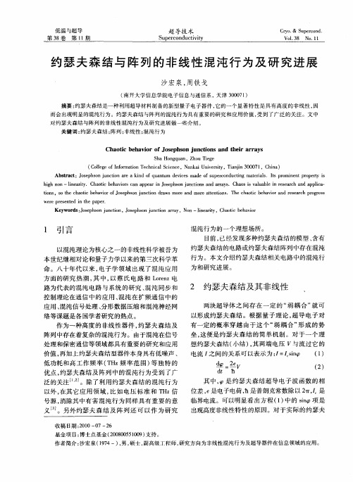
本 世纪继 相对论 和量子 力学 以来 的第 三次 科学革 命 。八十年 代 以来 , 电子学 领 域 出现 了混 沌应 用 方 面的研 究 热 潮 , 中 , 蔡 氏 电 路 和 Lr z电 其 以 oe n
路 为代表 的混沌 电路 与 系统 的研 究 、 沌 同步和 混
2 约瑟夫森结及其非线性
1 引 言
以混 沌理论 为核心行 为的一个 理想场 所 。 目前 , 已经 发现多 种约瑟 夫森结 的模 型 、 含有
约 瑟夫森 结 的电路或 约瑟夫 森结 阵列 中存 在混沌 行 为 。本 文介 绍约瑟夫 森结 相关 电路 中的混沌行
为 和研究进 展 。
( 开大学信息学院电子信息与通信 系,天津 30 7 ) 南 0 0 1 摘要 : 约瑟夫森结是一种利用超 导材料制备 的新型量子电子器件 , 它的一个 显著特性是具有 高度的非线性 , 因 而会 出现 明显 的混沌行为。约瑟夫森结与阵列的混沌行 为具有重要 的研究和应用价值 , 受到 了广泛 的关 注。文 中 对约瑟夫森结与阵列 的非线性混沌行为及研究进 展做一些介绍 。 关键词 : 约瑟夫森结 ; 阵列 ; 非线性 ; 7 昆沌行为
C a t e a iro oe ho u c o sa d tera ry h oi b h vo f sp snj n t n n h i ra s c J i
S a Ho g u n,Zh u Ti g h nqa o ee
( o e eo Ifr a o eh i l c n e a k i nvri , i j 0 0 , hn ) C l g f nom t n T c n a S i c ,N n a U i s y T a i 3 0 7 C ia l i c e e t nn 1
约瑟夫森结的电路模型及其在超导电子学中的应用
A src : ae n oe ho l i s a i ut dl fh sp snjn t ni it d c d h i bta t B sdo sp snr a o , r imoe o e oeho c o r u e .T e r J e tn cc t J u i sn o c—
关键 词 : 约瑟 夫森结 ; 电路 模 型 ; 混沌行 为 ; S Q电路 ; RF 相位 锁定 ;Q I S UD 中图分类 号 :N 1 , 5 1 4 T 7 0 0 1 . 文 献标识 码 : A 文章编 号 :6 35 9 ( 0 0 0 -7 -5 17 —6 2 2 1 ) 54 60
ti d li e nsr td wih smu a in r s ls,wh c s v l b e f rt e r s a c f s p r o d c ie h s mo e s d mo ta e t i l t e u t o ih i aua l o h e e r h o u e c n u t v
Th o e ft eJ s p s n J n to n t p iain n eM d lo h o e h o u cin a d i Ap l t si s c o
S e c ndu tV e t o c up r O c i e Elc r nis
S A H n —u n WA G Z e g Z O i g , H O Xnj , A G L n Te e Z A i—e F N a ,Y N S a-n — i i
- 1、下载文档前请自行甄别文档内容的完整性,平台不提供额外的编辑、内容补充、找答案等附加服务。
- 2、"仅部分预览"的文档,不可在线预览部分如存在完整性等问题,可反馈申请退款(可完整预览的文档不适用该条件!)。
- 3、如文档侵犯您的权益,请联系客服反馈,我们会尽快为您处理(人工客服工作时间:9:00-18:30)。
Home Search Collections Journals About Contact us My IOPscienceStructural and electrical characterization of ultra-thin SrTiO3 tunnel barriers grown over YBa2Cu3O7 electrodes for the development of high T c Josephson junctionsThis content has been downloaded from IOPscience. Please scroll down to see the full text.2012 Nanotechnology 23 495715(/0957-4484/23/49/495715)View the table of contents for this issue, or go to the journal homepage for moreDownload details:IP Address: 58.198.97.239This content was downloaded on 24/05/2014 at 08:23Please note that terms and conditions apply.IOP P UBLISHING N ANOTECHNOLOGY Nanotechnology23(2012)495715(6pp)doi:10.1088/0957-4484/23/49/495715Structural and electrical characterization of ultra-thin SrTiO3tunnel barriers grown over YBa2Cu3O7electrodes for the development of high T c Josephson junctionsL Avil´e s F´e lix1,M Sirena1,2,L A Ag¨uero Guzm´a n3,J Gonz´a lez Sutter3,S Pons Vargas3,L B Steren2,4,R Bernard5,J Trastoy5,J E Villegas5,J Bri´a tico5,N Bergeal6,J Lesueur6and G Faini71Centro At´o mico Bariloche,Instituto Balseiro—CNEA,Universidad Nacional de Cuyo,AvenidaBustillo9500,8400Bariloche,Rio Negro,Argentina2Consejo Nacional de Investigaciones Cient´ıficas y T´e cnicas,Avenida Rivadavia1917C1033AAJCABA,Argentina3Universidad de Concepci´o n,Victoria631,2613Concepci´o n,Chile4Centro At´o mico Constituyentes,Avenida Gral.Paz1499,San Mart´ın1650,Buenos Aires,Argentina5Unit´e Mixte de Physique CNRS/THALES,Universit´e Paris Sud11,F-91767Palaiseau Cedex,France6Laboratoire de Physique et d’Etude des Mat´e riaux,UMR8213/CNRS,ESPCI ParisTech,10rueVauquelin,Paris F-75005,France7LPN-CNRS,Route de Nozay,F-91460Marcoussis,FranceE-mail:lavilesf@Received11August2012,infinal form24October2012Published16November2012Online at /Nano/23/495715AbstractThe transport properties of ultra-thin SrTiO3(STO)layers grown over YBa2Cu3O7electrodeswere studied by conductive atomic force microscopy at the nano-scale.A very good control ofthe barrier thickness was achieved during the deposition process.A phenomenologicalapproach was used to obtain critical parameters regarding the structural and electricalproperties of the system.The STO layers present an energy barrier of0.9eV and anattenuation length of0.23nm,indicating very good insulating properties for the developmentof high-quality Josephson junctions.(Somefigures may appear in colour only in the online journal)1.IntroductionA superconductor–insulator–superconductor Josephson junc-tion(JJ)is formed by two superconductor electrodes separated by a very thin insulating barrier composed of a few atomic layers[1].Cooper pairs canflow through this barrier thanks to the coupling of the superconducting electrodes.If a constant voltage is applied on the junction,an alternating current with a frequency in the range of1–1000GHz can be generated in the system[2].These two particular phenomena have many technological applications,such as the fabrication of a voltage standard[3],SQUIDs and other magnetic sensors[4], quantum computing(qubits)[5],and the fabrication of ultra-fast superconducting microelectronics based on rapid singleflux quantum logic[6].However,the fabrication of a homogeneous JJ array is complicated,especially for highT c superconducting(HTSc)materials[7–9].A successful JJ technology requires an improvement and a better control of the JJ characteristics,in particular the JJ energy,i.e.the I c R n product,where I c is the critical current of the junction and R n its resistance in the normal state.This could be achieved with a better control of the barrier properties,reducing the thickness of the insulating barrier,in order to increase the superconducting coupling between the electrodes.In recent years,the improvement in microfabrication techniques has allowed the size of the operating devices to be reduced below the micro-scale.Moreover,recently,researchers from the Unit´e Mixte de Physique CNRS/Thales have developed a fabrication technique using AFM controlled nanoindentation for the development of nanojunctions[10].Typical sizes of these devices go from10×10nm2to50×50nm2, and with this size reduction the homogeneity of the barrier and the probability to obtain a working device should increase significantly.However,a good characterization of the insulating barrier at the nano-scale must be made in order to improve the performance of tunnel junction devices. We have recently developed a phenomenological approach using conductive atomic force microscopy(CAFM)[11,12] that allows one to obtain important electrical information to optimize the quality of JJ devices,e.g.the barrier thickness required to totally cover the superconducting electrodes and the physical properties of the barrier(its thickness distribution,the attenuation length and the energy barrier).In recent years,CAFM has become an extremely useful technique to study and characterize the insulating barriers of tunnel junction devices,such as magnetic tunnel junctions[13–15]or spinfilters.However,little work has been done using CAFM for the electrical characterization of insulating layers for the development of JJ[16].CAFM is a technique capable of performing local resistance measurements between the tip and the sample and allows one to obtain simultaneously the topography and the conductivity maps of different systems at the nano-scale[17,18].This technique also provides qualitative information about the insulating barrier homogeneity,directly detecting pinholes or hotspots,which can shortcut the electrodes reducing the quality of the JJ.The phenomenological approach used in this work is,basically,a generalization of the theoretical Simmons’model[19].Special attention was paid to analyze the influence of the surface defects in the topography and the conductivity map of these systems.We would like to stress that the use of the CAFM in the frame of this phenomenological approach allows one to obtain critical information about the structural and electrical properties of ultra-thin insulating layers,which are one of the key components not only of superconductor Josephson junctions but also of many other technological devices,such as magnetic tunnel junctions[20],multiferroic tunnel junctions and spinfilters[10],new memristors technologies[21]and tunneling electroresistance devices[22].Moreover,improved characterization methods of ultra-thin oxides are needed,as their importance continues to grow as new properties and new functionalities are discovered[23].2.Experimental detailsYBa2Cu3O7/SrTiO3(YBCO/STO)bilayers were grown on single-crystal(100)STO substrates by pulsed laser deposition with a KrF excimer laser(248nm)of780mW from stoichiometric ceramic targets.STO layers with thicknesses of0.4,0.8,1.2,1.6and2nm were deposited over YBCO electrodes with a thickness of75nm.The bilayers were grown in situ at664◦C using an oxygen pressure of0.355mbar. After deposition,the temperature of the sample was decreased to500◦C for an hour in order to assure the oxygen content of the YBCO and STO layers.Typical YBCO electrodes present a superconducting transition temperature of85K.CAFM measurements were performed at room tem-perature on a Veeco Dimension3100scanning probe microscopy AFM with a CAFM module and using a boron-doped diamond conductive tip(Bruker DDESP-10, spring constant=20–80N m−1)in contact mode.The CAFM tip was polarized with a positive voltage while the YBCO electrode was grounded.The minimum detectable current in the CAFM used is50pA,and the maximum current is480nA,under a bias voltage ranging from0.01to 12V.The CAFM is operated with a constant force(0.5V of deflection setpoint),with the laser reflecting always at the same position of the cantilever,and with a constant bias voltage to reducefluctuations in the mapping of the tunnel currents as a consequence of external parameters[16]. Different scan sizes and different scan orientations were used to rule out the presence of tip artifacts.CAFM images and I(V)curves were always taken in untouched areas in order to reduce the chemical modification of the surface due to the polarization voltage of the tip.I(V)curves for samples with different thicknesses of the insulating layer were obtained by holding the tip steadily in contact with the surface of the samples.Then the CAFM set up varies the applied voltage in the‘ramp’mode and measures the current for different values of the polarization voltage.In order to reduce thefluctuations of the I(V)measurements and the electrical contact noise, several I(V)curves(∼25measurement)were performed at different places on the samples and then averaged.3.Results and discussionFigure1shows the topographic(left)and CAFM(right) images measured simultaneously for YBCO/STO bilayers with different thicknesses of the insulating layer at a constant applied voltage.The scanning area is15×15µm2.In the electrical images,the bright areas indicate high tunneling currents.As expected,the current through the STO barrier decreases as the STO thickness increases.The samples present a very low roughness,∼0.5nm(∼1u.c.)and a low density of surface defects(∼0.07defµm−2),with heights going from 10to50nm.CAFM images show that the resistance through the grain boundaries of YBCO is higher than the resistance through the center of the grains.In general,higher values of tunneling current were detected at the center of the grain. Grains present a diameter between180and220nm with a separation between them in the range from80to120nm.Figure1.Topographic(left)and CAFM(right)15µm×15µm images of YBCO/STO bilayers grown over STO substrates with different STO thicknesses(2u.c.(a),3u.c.(b)and4u.c.(c)).The applied voltage was3V.CAFM current distributions(figure2)for the samples with STO thicknesses smaller than4u.c.present a high current peak that seems to correspond to the existence of pinholes in the barrier.However,the density of pinholes reduces rapidly for thicknesses greater than3u.c.The CAFM current distribution can be wellfitted with a log-normal distribution,as expected from the exponential decay of the tunneling current with the barrier thickness[24].The current distributionfitting for the sample with a barrier thickness of 3u.c.is not as good as thefitting for the other samples.The experimental data seem to show a double peak distribution (dotted lines infigure3),meaning thefitting with a single distribution peak(single line)is not as good as thefitting for the other samples.This is probably due to the existence of two areas with a slightly different thickness or a small change in the tip–surface resistance during the scan.However, the effect is small and was not observed for the other samples.The current distribution widths obtained from the fits corresponds to a barrier thickness distribution width of σd∼0.6nm(1.5u.c.),in agreement with the observed topographic roughness of the samples.The evolution of the current distributions as a function of the barrier thickness shows the good control and reproducibility of the insulating layers grown by pulsed laser deposition.Figure3shows characteristic I(V)curves for YBCO/STO bilayers with different thicknesses of the insulating barrier, obtained with the CAFM.The experimental data arefitted using a phenomenological approach based on the Simmons model[19]:ln(I(V,d))=A0(d)+α(d)ln V−B(d)V.(1)We have used threefitting parameters A0,αand B that depend on the barrier nature or its thickness(d).In the Simmons model,for polarization voltages higher than theFigure2.Current distributions for YBCO/STO bilayers.The curves correspond to different thicknesses of the barrier( =5u.c., =4u.c., =3u.c.and =2u.c.)at3V.The lines arefittings using the log-normal distribution(seetext).Figure3.I(V)curves for the YBCO/STO bilayers for different thicknesses of the STO barrier.The solid lines are linearfits of theexperimental data(ln I=A0+αln V−B(d)V ).The inset presents theaverage values of A0andαas a function of the barrier thickness(d) obtained from thefitting of the I(V)curves.energy of the barrier,α=2.As shown in the inset offigure3, A0andαdepend linearly on the barrier thickness.B was found to be smaller than the experimental resolution and was assumed to be zero.So,in general,for voltages higher than 1V,we can rewrite equation(1)as[11,12]:I=e a0Vα0e−dλwithλ=1|a |−α ln V,(2)whereλis the electronic attenuation length of the carriers in the barrier and a0=A0(d=0);α0=α(d=0);a =∂A0∂d<0 andα =∂α∂d.In order to reduce the currentfluctuations and to obtain accurate values of A0andα,several I(V)curves were measured,placing the conductive tip in different zones of the sample and averaging.The I(V)curves show a more abrupt change of the tunneling current as a function of the polarization voltage than the expected behavior predictedby parison between the values ofαas a function of the attenuation length for three systems modeled with the same phenomenological approach.The curves correspond to different thicknesses of the barrier( =2u.c., =4u.c., =5u.c.).Inset: attenuation length(open squares)and energy barrier(open circles) as a function of the polarization voltage for the YBCO/STO bilayers.the Simmons model[19].Indeed,for the samples studied in the present work,α0varied between4and7,larger than the theoretical value(α0=2)corresponding to the high-voltage tunneling regime(V>φ/e,whereφis the energy barrier of the junction)[19].To obtainλ,we have plotted ln(I/Vα0)= a0−d/λas a function of d for different polarization voltagesand a linearfit of the experimental data was performed.The obtained value ofλ=0.23nm is in good agreement with the values reported in the references mentioned above[11,12], for similar insulating barriers.The value of the attenuation length increases when the applied voltage increases,with a value of0.23nm for1.25V(inset offigure4).Once the attenuation length is obtained,the energy barrier can be estimated,by considering a rectangular barrier shape,for different applied voltages.Under these assumptions,in the Simmons model[18,19],the energy barrier is given by φ=(3he8π√2m∗Vλ)2/3,where h is the Planck constant,m∗is the effective mass of the charge carriers,e is the electron charge and V is the applied voltage.m∗is given by the band structure of STO,and for the present calculations it has been considered that m∗=m e(giving an upper limit of the energy barrier).The energy barrier varies between0.8and1.2eV,being around 0.90eV at1.25V(inset offigure4),higher than the values reported in the literature in similar systems[12,18,25].The variation of the energy barrier could be related to reproducible uncertainties of the measurements,since no change ofφwith the polarization voltage is usually expected.It should be noticed that the assumption of the Fowler–Nordheim regime is not always satisfied for the samples with thinner barriers.This is probably why the I(V)curves for the samples with thicker barriers(i.e.5u.c.)and higher voltages present a better linear behavior than the samples with thinner barriers.However,this effect seems to be small.As mentioned before,the experimental data show a faster increase of the tunneling current with increasingapplied voltage than the behavior predicted by the Simmonsmodel.According to this model,in the Fowler–Nordheim(FN)regime,the current follows a V2law(α0=2).This square dependence of the tunneling current with theapplied voltage arises from the assumption that,for thehigh-voltage regime,the effective thickness of the rectangularpotential barrier,d eff,decreases linearly as the applied voltageincreases and d eff=dφ/eV[19].However,it seems thatthis is not the case for this system,and a similar behaviorwas observed for Nb/Ba0.05Sr0.95TiO3(BSTO)[12]andLa0.75Sr0.25MnO3(LSMO)/BSTO bilayers[11].Moreover,experimental evidence indicates thatα0depends on theinsulating nature of the barrier.Therefore,in analogy tothe Simmons model,an effective thickness of the potentialbarrier of the form d eff=dφ/eVα0/2(generallyα0>2)was considered.This indicates a decreasing effective thickness ofthe insulating barrier as the value ofα0increases,and alsogives a qualitative idea about the deformation of the effectivebarrier for the charge carriers.For high applied voltages,andfor a given d(e.g.afixed value ofα0),the tunnel transporttakes place through an effective barrier thinner than thatexpected in the Simmons model due to d eff∝1/Vα0/2.Asimilar result is obtained when the effect of the image forceis considered[19].The image force rounds the corner ofthe barrier,reducing its effective thickness and increasing thetunneling current of the junction.It was noted by Simmonsthat the image potential is a hyperbolic function,which resultsin an elliptic integral when included in the general equationto calculate the tunneling current,and can only be solvednumerically.The phenomenological method proposed in thiswork gives a simple way to evaluate the importance of theimage forces in these systems.The increase ofα0withincreasing barrier thickness seems to indicate that the more‘insulating’(thicker insulating barriers)the system is,themore abrupt(higherα)is the change of the tunneling currentwith the applied voltage.In order to test this hypothesis,αwas plotted as function of the attenuation length,λ,for threedifferent systems,YBCO/STO,Nb/BSTO and LSMO/BSTO(figure4).Thefigure shows that for these systems,αincreasesas the attenuation length decreases,indicating that‘moreinsulating’materials with lower attenuation lengths,presenta more important change of the tunneling current with theapplied voltage.A similar effect was observed theoretically bySimmons[19],when the influence of the barrier’s dielectricconstant was considered to calculate the resistance of thetunnel junction as function of the applied voltage.The originof this phenomenon is not clear and more work is needed inorder to provide a new insight about the tunneling mechanismin these systems.4.ConclusionsWe have used a phenomenological approach based on theSimmons model to analyze the electrical transport throughultra-thin SrTiO3layers grown over YBa2Cu3O7electrodes.The proposed method helps one,in a direct way,to study andto optimize the growth of insulating barriers over high criticaltemperature superconductor electrodes in order to improve the performance and application of high T c Josephson junctions. We have found that the tunneling of the carriers seems to be the main mechanism for the electrical transport in these systems.In general,a STO barrier thickness of at least1.6nm (4u.c.)is required to obtain a good insulation of the YBCO electrode for small areas.The SrTiO3layers present an energy barrier of0.9eV,with an attenuation length of0.23nm, indicating their good insulating properties.The deposition method allows the growth of high-quality ultra-thin STO layers over high T c superconducting electrodes,with a very good control of the barrier thickness,for the fabrication of Josephson junctions.AcknowledgmentsThe authors would like to thank R Benavides for his extraordinary technical support.The authors would also like to recognize the important work,help and support from Dr J Guimpel and Dr H Pastoriza for the use of micro-and nanofabrication facilities and A Butera for the critical reading of the manuscript.This work was partially supported by the ANPCYT(PICT PRH2008-109),Universidad Nacional de Cuyo(06/C328)and the international cooperation program MINCyT-ECOS(France)A10E05.J Trastoy acknowledges the support from Fundaci´o n Barri´e(Galicia,Spain). References[1]Josephson B D1962Phys.Lett.1251[2]Barone A and Paterno G1982Physics and Applications of theJosephson Effect(New York:Wiley)pp309–24[3]Benz S P,Hamilton C A,Burroughs C J,Harvey T E andChristian L A1997Appl.Phys.Lett.711866[4]Adachi S,Tsukamoto A,Oshikubo Y,Hato T andTanabe K2011Physics C4711258[5]Nakamura Y,Nakamura Y,Terai H,Inomata K,Yamamoto T,Qui W and Wang Z2011Appl.Phys.Lett.99212502 [6]Hassel J,Helist¨o P,Sepp¨a H,Kunert J,Fritzsch L andMeyer H G2006Appl.Phys.Lett.89182514[7]Bergeal N,Lesueur J,Sirena M,Faini G,Aprili M,Contour J-P and Leridon B2007J.Appl.Phys.102083903 [8]Hamilton Clark A,Burroughs Charles J and Benz Samuel P1997IEEE Trans.Appl.Supercond.73756[9]Bernard R,Briatico J,Sirena M,Crete D G andContour J-P2007IEEE Trans.Appl.Supercond.173589 [10]Bouzehouane K,Fusil S,Bibes M,Carrey J,Blon T,Le Dˆu M,Seneor P,Cros V and Vila L2003Nanoletters31599 Bouzehouane K,Fontcuberta J,Barth´e l´e my A andFert A2007Nature Mater.6296–302[11]Sirena M2011J.Appl.Phys.110063923[12]Sirena M,Avil´e s F´e lix L,Carvacho Vera G A,Navarro Fern´a ndez H L,Steren L B,Bernard R,Bri´a tico J,Bergeal N,Lesueur J and Faini G2012Appl.Phys.Lett.100012602[13]Canizo-Cabrera A,Li Simon C,Shu M-F,Lee J-M,Garcia V V,Chen C C,Chen J C,Wu J C,Takahashi M andWu T-H2005IEEE Trans.Magn.40887[14]Luo E Z,Wong S K,Pakhomov A B,Xu J B,Wilson I H andWong C Y2001J.Appl.Phys.905202[15]Ando Y,Kameda H,Kubota H and Miyazaki T2000J.Appl.Phys.875206[16]Lang K M,Hite D A,Simmonds R W,McDermott R,Pappas P and Martinis J M2004Rev.Sci.Instrum.752726[17]Bhutta K M,Schmalhorst J and Reiss G2009J.Magn.Magn.Mater.3213384[18]Infante C,Sanchez F,Laukhin V,P´e rez del Pino A,Foncuberta J,Bouzehouane K,Fusil S andBarth´e lemy A2006Appl.Phys.Lett.89172506[19]Simmons John G1963J.Appl.Phys.341793[20]Tsoi M2008Nature Phys.417[21]Chanthbouala A et al2012Nature Mater.11860[22]Garc´ıa V,Fusil S,Bouzehouane K,Enouz-Vedrenne S,Mathur N D,Barth´e l´e my A and Bibes M2009Nature48081[23]Warusawithana M P et al2009Science324367[24]Bardou F1997Europhys.Lett.39239[25]Fix T,Da Costa V,Ulhaq-Bouillet C,Colis S,Dinia A,Bouzehouane K and Barth´e l´e my A2007Appl.Phys.Lett.91083104。