AM软件使用说明
AM软件功能研究及实船设计应用

AM软件功能研究及实船设计应用大连中远船务工程有限公司大连116113 栾丰一陈佳名潘秋艳摘要全球造船设计领域最先进的三维设计软件之一Aveva Marine(AM),已成功用于大连中远船务的造船项目。
本文就92.5K项目的应用,对软件的特性、基本功能、引进消化、二次开发、实船应用、展望建议等进行简要叙述。
关键词:软件消化吸收二次开发一、背景概要中远船务为了在造船领域实现跨越式发展,2006年11月从英国AVEVA公司引进世界先进造船设计软件之一VENTAGE MARINE(VM),2007年11月软件升级更名为AVEVA MARINE(AM)。
因为原瑞典的TRIBON公司已被AVEVA并购,且TRIBON系统已不再做开发升级,从长计议,中远船务成为VM/AM软件在国内造船业首家用户。
2008年2月,在经过一系列调研论证后,确定在92500DWT散货船的生产设计中全面应用AM。
二、软件特性AM软件是两种被实践证明最好的技术融合为一个具有世界领先水平的海事工业解决方案,即船体采用M3船体技术和舾装采用PDMS技术。
这两种技术融合后的产品AM具有解决复杂工程设计和管理的能力;提高了工程项目设计效率和数据质量、增强了数据安全性、改进项目业务协调的效率等增强性特征。
AM软件基于最新的.NET技术的交互界面、支持多用户工作和面向对象的数据库结构、支持多级别数据管理(地域之间、专业之间、人员之间、设计方案之间)、可实现异地同步设计、可实时干涉检查的纯三维设计软件。
支持对设计元素操作类别、设计元素属性修改等团队和人员的权限控制。
具有灵活的设计方法,交互的操作模式及开放的开发环境。
三、基本功能AM软件提供了极强的专业化设计功能,船体、管系、电气、铁舾、通风等适合船舶设计与建造的设计流程。
船体专业提供从初步设计、详细设计到生产设计的完整的解决方案且初步设计、详细设计的数据可以直接被生产设计使用,最大限度地减少重复劳动。
AM—调制与解调仿真
引言本次实践开设的计算机课程设计为软件仿真,利用matla b编写程序建立M文件对计算机实验进行仿真。
随着通信技术的发展日新月异,通信系统也日趋复杂,在通信系统的设计研发过程中,软件仿真已成为必不可少的一部分.随着信息技术的不断发展,涌现出了许多功能强大的电子仿真软件,如Work be enc h、Pr ote l、Sys temview 、Matlab 等。
虚拟实验技术发展迅速,应用领域广泛,一些在现实世界无法开展的科研项目可借助于虚拟实验技术完成,例如交通网的智能控制、军事上新型武器开发等。
调制就是使一个信号(如光等)的某些参数(如振幅、频率等)按照另一个欲传输的信号(如声音、图像等)的特点变化的过程.解调是调制的逆过程,它的作用是从已调波信号中取出原来的调制信号。
对于幅度调制来说,解调是从它的幅度变化提取调制信号的过程。
对于频率调制来说,解调是从它的频率变化提取调制信号的过程。
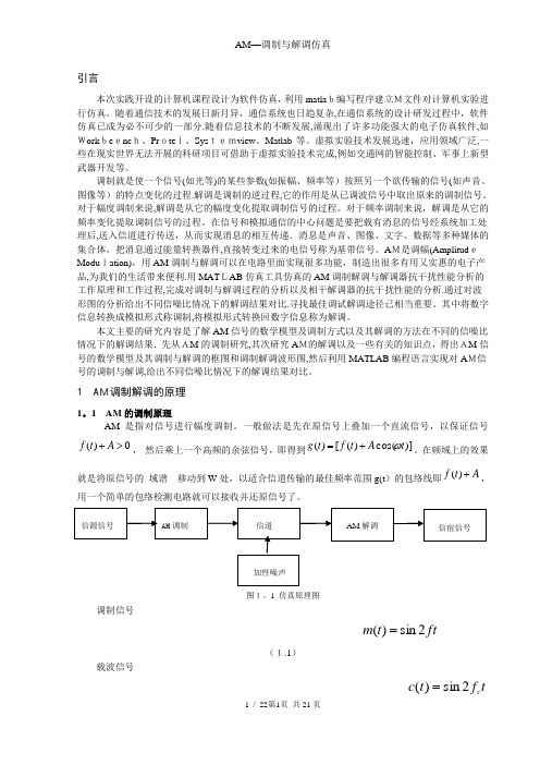
在信号和模拟通信的中心问题是要把载有消息的信号经系统加工处理后,送入信道进行传送,从而实现消息的相互传递.消息是声音、图像、文字、数据等多种媒体的集合体。
把消息通过能量转换器件,直接转变过来的电信号称为基带信号。
A M是调幅(Amplitud eModu lation),用AM 调制与解调可以在电路里面实现很多功能,制造出很多有用又实惠的电子产品,为我们的生活带来便利.用MAT LAB 仿真工具仿真的AM 调制解调与解调器抗干扰性能分析的工作原理和工作过程,完成对调制与解调过程的分析以及相干解调器的抗干扰性能的分析.通过对波形图的分析给出不同信噪比情况下的解调结果对比.寻找最佳调试解调途径已相当重要。
其中将数字信息转换成模拟形式称调制,将模拟形式转换回数字信息称为解调。
本文主要的研究内容是了解AM 信号的数学模型及调制方式以及其解调的方法在不同的信噪比情况下的解调结果.先从AM 的调制研究,其次研究A M的解调以及一些有关的知识点,得出AM 信号的数学模型及其调制与解调的框图和调制解调波形图,然后利用MATLAB 编程语言实现对A M信号的调制与解调,给出不同信噪比情况下的解调结果对比。
AMPCI-9111使用说明书

AMPCI-9111通用数据采集控制板使用说明书2001/03一、概述AMPCI-9111板是PCI总线通用采集控制板,该板可直接插入具备PCI插槽的工控机或个人微机,构成模拟量电压信号、数字量电压信号采集、监视输入和模拟量电压/电流信号输出、数字量信号输出及计数定时系统。
AMPCI-9111板为用户提供了单端32路/双端16路模拟量数据采集输入通道, 模拟量输入通道具有程控放大功能,2路12Bit模拟量电压或电流信号输出,16Bit TTL数字量输入和16Bit TTL数字量输出,配接AMPCD821光隔端子板实现光隔I/O,可直接驱动继电器, 3路16位计数定时通道(一片82C54),计数频率8M,板内自带基准时钟4M,82C54的0、 1、2通道均引至输出插座J2,可构成脉冲计数、频率测量、脉冲信号发生器等电路。
对AMPCI-9111板的所有读写操作均为16Bit即D00~D15,当对82C54进行读写时只有D00~D07有效,同样A/D转换数据一次读入的为B00~B11。
二、性能和技术指标2.1 性能•模拟信号输入A/D分辩率: 12Bit•模拟信号通道: 单端32路/双端16路•模拟信号输入程控放大倍数: 1/2/4/8 (B型为1/10/100/1000)•模拟信号输出D/A分辩率: 12Bit•模拟信号输出通道: 2路•数字量输入/输出: 16Bit DI/16Bit DO ;TTL/COMS兼容•计数定时通道: 3路16BIT• A/D转换触发工作方式: 软件触发• A/D转换数据传输方式: 查询方式2.2 技术指标•输入电压范围: ±5V、0-10V、±10V•输入阻抗: > 100 MΩ• A/D转换时间: 8.5uS• A/D转换精度: 优于±0.1%(10V满量程)•输出电压范围: ±5V、0-5V、0-10V•输出电流范围: 0-10mA 、4-20mA•内部时钟基准: 4MHz三、使用3.1本板A/D转换工作过程描述AMPCI-9111板的A/D转换是通过软件来控制和启动A/D转换的<1>使用时首先应程序设定要进行A/D转换的通道号,即要对哪一通道进行A/D转换,该写操作见后面《寄存器功能描述》的(1)节: “模拟输入通道选择、增益选择寄存器”,该寄存器I/O地址Offset=00H ,“Offset”是相对地址的偏移量,为该寄存器的I/O地址(详细对“Offset”的读写操作见软件说明部分)<2>程序设定完要进行A/D转换的通道号和放大倍数后,需执行程序启动A/D转换操作,A/D转换器才开始转换,即再执行《寄存器功能描述》的(2)节,“启动A/D转换”,该写操作的I/O地址 Offset=02H,该操作为软件触发启动一个周期的A/D转换,若A/D转换的放大倍数不是1倍,应在设定“模拟输入通道选择、增益选择寄存器”操作后,适当加几个μS的延时以给程控放大器足够的建立时间,再执行启动A/D转换操作,以保证精度<3>启动A/D转换后,通过软件查询A/D转换完成状态标志位,见《寄存器功能描述》的(3)节,“查询A/D 转换状态位+A/D转换数据”,“Z”该位为1,说明A/D转换器正在进行转换,不可读取A/D转换数据,继续查询该位,若该位为0,说明A/D转换已完成,可读取A/D转换数据,该读操作的I/O地址 Offset=0AH,标志位Z对应该标志寄存器数据线D15-D00的D15,当查询A/D转换完成状态标志位“Z”位为0时,此时读取该口的B11-B00 即为A/D转换数据3.2本板D/A转换工作过程描述进行D/A转换时只需向相应的I/O端口写12BIT数据即可,如对D/A1进行转换,将数据B11-B00写入D/A1数据寄存器offset=06H端口即可3.3本板结构如下:主要元件位置、信号输入/输出插座及跳线选择定义AMPCI-9111/9111BJ1: 模拟量输入输出37P孔式D型插座J2: 数字量计数定时输入输出50P双排针插座JP1/JP2: 单双端输入方式设定JP3: A/D输入范围设定JP6: D/A1输出方式设定JP7: D/A2输出方式设定3.4 J1模拟信号输入/输出插座定义:<1>模拟输入单端方式引线定义见下:⊙ 19 GNDGND 37 ⊙⊙ 18 D/A-1 +12V 36 ⊙⊙ 17 D/A-2通道32 35 ⊙⊙ 16 通道16通道31 34 ⊙⊙ 15 通道15通道30 33 ⊙⊙ 14 通道14通道29 32 ⊙⊙ 13 通道13通道28 31 ⊙⊙ 12 通道12通道27 30 ⊙⊙ 11 通道11通道26 29 ⊙⊙ 10 通道10通道25 28 ⊙⊙ 9 通道9通道24 27 ⊙⊙ 8 通道8通道23 26 ⊙⊙ 7 通道7通道22 25 ⊙⊙ 6 通道6通道21 24 ⊙⊙ 5 通道5通道20 23 ⊙⊙ 4 通道4通道19 22 ⊙⊙ 3 通道3通道18 21 ⊙⊙ 2 通道2通道17 20 ⊙□ 1 通道1印制板D/A-1: 模拟输出通道1D/A-2: 模拟输出通道2GND: 模拟输入/输出地单端方式时32路模拟输入信号连接到通道n输入端,所有信号的地端接到GND端,下图所示CH00(1通道)输入 CH01(2通道) Vi 被测信号端 .口 . Vi.CH1F(32通道)ViGND(地线)单端方式时32路模拟输入信号接线示意图单端输入时通道代码与选择通道对应关系如下:<2>模拟输入双端方式引线定义见下:双端方式时16路模拟输入信号连接到通道正端和通道负端,信号的负端经电阻接到GND端,下图所示⊙ 19 GNDGND 37 ⊙⊙ 18 D/A-1+12V 36 ⊙⊙ 17 D/A-2通道16- 35 ⊙⊙ 16 通道16+通道15- 34 ⊙⊙ 15 通道15+通道14- 33 ⊙⊙ 14 通道14+通道13- 32 ⊙⊙ 13 通道13+通道12- 31 ⊙⊙ 12 通道12+通道11- 30 ⊙⊙ 11 通道11+通道10- 29 ⊙⊙ 10 通道10+通道9- 28 ⊙⊙ 9 通道9+通道8- 27 ⊙⊙ 8 通道8+通道7- 26 ⊙⊙ 7 通道7+通道6- 25 ⊙⊙ 6 通道6+通道5- 24 ⊙⊙ 5 通道5+通道4- 23 ⊙⊙ 4 通道4+通道3- 22 ⊙⊙ 3 通道3+通道2- 21 ⊙⊙ 2 通道2+通道1- 20 ⊙□ 1 通道1+印制板现场信号双端方式时16路模拟输入信号接线示意图双端使用说明:双端输入时信号加在CHn+和CHn-之间,模拟输入采用双端方式时,负输入端应与GND之间接一只几十KΩ~几百KΩ的电阻(信号源内阻小于100Ω时,该电阻应为信号源内阻的1000倍,当信号源内阻大于100Ω时,该电阻应为信号源内阻的2000倍),从而为仪表放大器输入电路提供偏置,见上图所示双端输入时通道代码与选择通道对应关系如下(双端时只有16个通道):3.5 数字量和计数定时器输入输出插座J2定义:J2为50P双排针插座GND 50 ⊙⊙ 49 GND+5V 48 ⊙⊙ 47 +5VCLK2 46 ⊙⊙ 45 OUT2GATE2 44 ⊙⊙ 43 CLK1GATE1 42 ⊙⊙ 41 OUT1 OUT0 40 ⊙⊙ 39 CLK0GATE0 38 ⊙⊙ 37 ФGND 36 ⊙⊙ 35 GND+5V 34 ⊙⊙ 33 +5VPB07 32 ⊙⊙ 31 PB06PB05 30 ⊙⊙ 29 PB04PB03 28 ⊙⊙ 27 PB02PB01 26 ⊙⊙ 25 PB00PB08 24 ⊙⊙ 23 PB09PB10 22 ⊙⊙ 21 PB11PB12 20 ⊙⊙ 19 PB13PB14 18 ⊙⊙ 17 PB15PA07 16 ⊙⊙ 15 PAO6PA05 14 ⊙⊙ 13 PAO4PA03 12 ⊙⊙ 11 PAO2PA01 10 ⊙⊙ 9 PAO0PA08 8 ⊙⊙ 7 PA09PA10 6 ⊙⊙ 5 PA11PA12 4 ⊙⊙ 3 PA13PA14 2 ⊙□ 1 PA15插座J2定义见图示其中:PAO0~PA15: 16bit数字量输出PB00~PB15: 16bit数字量输入+5V: 机内PCI总线+5VGND: 机内地GATE0: 计数器通道0门控GATEOUT0: 计数器通道0输出端CLK0: 计数器通道0时钟输入端GATE1: 计数器通道1门控GATEOUT1: 计数器通道1输出端CLK1: 计数器通道1时钟输入端GATE2: 计数器通道2门控GATEOUT2: 计数器通道2输出端CLK2: 计数器通道2时钟输入端3.6 跨接线选择定义:<1> JP1/JP2: JP1和JP2用来设置A/D模拟输入采用单端方式/双端方式①A/D输入采用单端方式时JP1/JP2按如下设置(出品状态):□○○○○ JP1 ; 即JP1的2和3短接, 4和5短接 1□○○○○○ JP2 ; 即JP2的2和3短接, 5和6短接1② A/D输入采用双端差分方式时JP1/JP2按如下设置:□○○○○ JP1 ; 即JP1的1和2短接, 3和4短接 1□○○○○○ JP2; 即JP2的1和2短接, 4和5短接 1<2>JP3 ;JP3用于设置A/D输入范围;可分别设置①-5V~+5V; ②0~+10V; ③-10V~+10V① -5V ~ +5V 输入范围时按如下设置(出品状态):○○○○2 ○□ 1 JP3; 即JP3的1和3短接, 4和6短接② 0 ~ +10V 输入范围时按如下设置:○○○○2 ○□ 1 JP3; 即JP3的1和3短接, 2和4短接③ -10V ~ +10V 输入范围时按如下设置:○○○○2 ○□ 1 JP3; 即JP3的3和5短接, 4和6短接<3> JP6与JP7JP6与JP7分别用来设置D/A1输出和D/A2输出的输出方式, JP6与JP7设置方式相同,可分别设置① D/A输出电压方式 -5V ~ +5V(出品状态):3○○○○○○○○○○□○○○○即(3,6);(9,12);(10,13)短接1 JP6/JP7② D/A输出电压方式 0V ~ +5V:3○○○○○○○○○○□○○○○即(3,6);(12,15);(10,13)短接1 JP6/JP7③ D/A输出电压方式 0V ~ +10V:3○○○○○○○○○○□○○○○即 (3,6); (10,13) 短接1 JP6/JP7④ D/A输出电流方式 0 ~ 10mA:3○○○○○○○○○○□○○○○即 (2,3); (7,8);(12,15) 短接1 JP6/JP7⑤ D/A输出电流方式 4 ~ 20mA:3○○○○○○○○○○□○○○○即 (2,3); (4,5); (7,8);(11,14) ;(12,15) 短接1JP6/JP73.7 I/O寄存器功能描述①: 模拟输入通道选择、增益选择寄存器(写操作)Offset=00H,Offset:相对地址的偏移量,即该写操作的I/O地址(详细对Offset=##H I/O端口的读写操作见后面软件说明部分,后同)G2~G0:程控放大增益选择位,意义见下:G1 G0 程控放大增益倍数 B型程控放大增益倍数(此时放大器为PGA202)0 0 1 10 1 2 101 0 4 1001 1 8 1000C4~C0: 模拟信号输入通道选择位 (注:单端方式时)C4 C3 C2 C1 C0 通道代码通道号0 0 0 0 0 00H 通道10 0 0 0 1 01H 通道20 0 0 1 0 02H 通道3...... ....... .1 1 1 1 0 1EH1 1 1 1 1 1FH 通道32注:双端方式时只有C3~C0有意义,此时只有16个通道,C4位无意义②启动A/D转换 (写操作)Offset=02H,Offset是相对地址的偏移量,该写操作的I/O地址D15~D00 此时无意义,软件设定通道和增益后需执行启动A/D转换,即执行对Offset=02H的写操作③查询A/D 转换状态位+A/D转换数据 (读操作)Offset=0AH Offset:相对地址的偏移量,该读操作的I/O地址读Offset=0AH时数据对应表:Z: A/D 转换状态位 Z=1, A/D转换器正在进行转换Z=0, 转换结束,可以读取本次A/D转换数据B11~B0 : 本次A/D转换数值在用户应用程序执行启动A/D转换后,应查询”Z”标志位, 当Z=1时A/D转换器正在进行转换,处于忙状态, 当Z=0时A/D转换结束,此时读回的数据B11-B00为有效的A/D转换值④ D/A1 模出转换数据寄存器 (写操作)Offset=06H, Offset:相对地址的偏移量,对D/A1写操作的I/O地址D/A1输出数据对应表:X: 未用位B11~B00: D/A1转换12Bit数据,输出D/A1时向Offset=06H写入B11~B00数值即可⑤D/A2 模出转换数据寄存器 (写操作)Offset=08H, Offset:相对地址的偏移量,对D/A2写操作的I/O地址D/A2输出数据对应表:X: 未用位B11~B00: D/A2转换12Bit数据,输出D/A2时向Offset=08H写入B11~B00数值即可⑥16位PA口TTL数字量输出寄存器(写操作)Offset=0CH, Offset:相对地址的偏移量,该写操作的I/O端口地址输出寄存器数据格式:A15~A00 : 16Bit数字量输出,对应J2的PA15~PA00⑦: 16位TTL数据输入寄存器 (读操作)Offset=0EH , Offset:相对地址的偏移量,该读操作的I/O地址输入寄存器数据格式:B15~B00 : 16Bit数字量输入, 对应J2的PB15~PB00⑧计数定时器8254的I/O地址分配(读操作+写操作)Offset=10H-16H, Offset是相对地址的偏移量,具体I/O地址分配见下表, 对82C54的所有读写操作只有D7~D0 有意义,编程时请注意具体对82C54的工作方式设定请参阅INTEL8253手册等相关资料AMPCI-9111读写I/O操作命令表:3.8 调整电位器定义PR1: 程控放大器增益输出调整电位器PR2: A/D转换单极性零偏移调整电位器PR3: A/D转换双极性零偏移调整电位器PR4: A/D转换满量程调整电位器PR5: D/A输出电流方式基准源-2.5V调整电位器PR6: D/A1零偏移调整电位器PR7: D/A1满量程调整电位器PR8: D/A2零偏移调整电位器PR9: D/A2满量程调整电位器PR10: D/A输出基准源+5V调整电位器3.9校准①A/D部分校准a.程控放大器调整:软件设置放大倍数8倍,任一通道接一500mV电压,调整PR1 使PGA202的12脚输出为4.000V(出品时已调整)b.单极性输入0~+10V:任一通道对地短接,调整PR2,使转换值为001H;输入任一通道接5V,调整PR4,使转换值为800H;c.双极性输入-5V~+5V:任一通道对地短接,调整PR3,使转换值为800H;输入任一通道4.997V调整PR4使转换值为FFEH;需要注意的是此时A/D转换的零点与满度需反复调整d.双极性输入-10V~+10V:任一通道对地短接,调整PR3,使转换值为800H;输入任一通道10V调整PR4使转换值为FFEH;同样需要注意的是此时A/D转换的零点与满度需反复调整② D/A部分校准基准源调整: 调整PR10使336-5V输出+5.000V,出厂时已调整。
MacamV3软件说明书-11报表工具
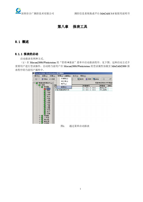
第八章报表工具8.1概述8.1.1报表的启动启动报表有两种方式。
(1)在Macam2000sWorkstation的“管理 报表”菜单中启动报表程序,见下图。
这种启动方式不需要用户进行登录操作,自动将当前用户在Macam2000sWorkstation的登录属性加载至MACAM2000报表程序的当前用户属性中。
图1.通过菜单启动报表图2.报表启动后(2)直接在“开始”菜单中运行MACAM2000报表程序,见下图。
这种方式需要核对用户权限,此时会出现登录对话框,需要输入正确的用户名和密码才能继续操作。
图3.在“开始”菜单中运行MACAM2000报表程序8.1.2报表界面报表程序的初始运行界面下图所示。
图4. 运行界面利用工具栏1或工具栏2可以实现不同的报表功能,包括报表输出打印、报表参量定义、报表格式定义和定时打印。
其中点击在工具栏1中的“退出”可以退出该报表程序。
在“报表类型”区可以根据用户需要选择不同的报表类型,同时在“报表显示”区显示不同类型的报表。
系统信息显示当前进入报表程序的用户名,以及该用户的权限,还有监控中心的说明和当前日期。
显示方式有四种,如图所示。
用鼠标点击下拉图标,选中相应的显示方式,则对应不同的界面。
选择不同的显示方式对应在报表显示区有不同的显示。
跟windows 的操作相同,不在赘述。
8.1.3 报表的分类在报表运行程序的“报表类型”中有报表类型的显示,包括实时报表、日报表、月报表、年报表和时间段报表。
实时报表如果需要得到某一个当前时刻的监控设备的实时报表数据,可以选择实时报表,在“报表显示”区双击要查询的报表(图5),等待程序运行完毕后可以得到当前报表的各项实时数据(图6)。
图5.实时报表选择图6.实时报表结果在上图中显示的是要打印的一个实时报表,包括报表名称“蓄电池组测试记录”,采集报表数据的时间(2003年5月20日9:53:18),监控系统的说明,需要的实时数据。
AM 编程软件介绍语法说明及实例
点击 OnLine Tree
点击右键 Refresh System 涮新在线更表
所有系统里面的设置都会显示出来,而且状态栏也相应的变绿。
也可以把 SRC 后缀后改成 RAR 后缀名,直接用压缩包的格式打开.
如何对继电器操作程序编写
我们要实现的是把下触摸屏或面板的按钮就实现继电器的开关动作 下面是定义的一个控制面板和 NI2100 设备上的继电器接口进行控制,如下图:
下面定义了一个自定义变量供下面的方法三使用:
下图功能为:按下按钮 11 打开继电器 3,如果继电器 3 接的是灯光的控制,则 打开灯光,如果是某设置的电源刚是控制设备的电源开,按下按钮 12 则是关闭, 按下按钮 13 的功能为,按一下开,再按一下关,一直循环下去。有如下三种方 法,如下图:
下面是触摸屏或按钮状态跟着程序走,看到按钮状态,相应的也就知道了继电 器的开关状态
如何实现矩阵程序编程实例
实现 8X8 矩阵的自由切换,先选择输入源,再选择输出源,可以一次性选择多个 输出源,如下图:
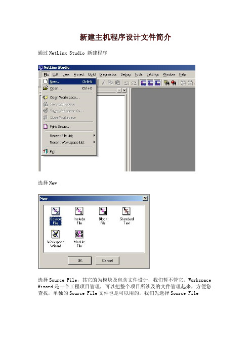
是否创建新文件,选择 Yes 选择,主机的标准模版,网络型主机则选择 NetLinx Standard Template
输入文件名 选择要保存的路径,按下一步。 点击完成,创建出新文件。
把蓝色的字给收起来,总体上我们可以看出分如下几块:
PROGRAME_NAME 为文件 DEFINE_DEVICE 为定义要控制设计的控制接口 DEFINE_CONSTANT 为定义常量 DEFINE_TYPE 为定义类型文件 DEFINE_VARIABLE 为定义变量
amibios设置全程图解(AM...
ami bios 设置全程图解(AMI BIOS settings throughout thediagram)Main (system settings)System time system time settingsSystem date date setAMIBIOS BIOS informationProcessor CPU InformationSystem memory memory informationAdvanced (advanced settings)Set the jumperfree cunflguratfon CPU memory parametersSet the CPU configuration CPUChipset chip setOnboard Devices Configuration integrated hardware device set The PCIpnp PCI setting deviceUSB Configuration USB device setInstant Music Configuration start free music setConfigure system frequency/voitageAI Overclock tuner CPU intelligent frequency settingPerformance Mode enhanced modeloptionSet manual ManualStandard standard modeOverclock 5% step overclockingConfigure System Frequency/VoltageCPU External Frequency {MHz} [xxxx] CPU FSB setDRAM Frequency [Auto] memory frequency settingsAGP/PCI Frequency {MHz} [Auto]AGP/PCI frequency setting equipmentCPU VCore Voltage [Auto] CPU core voltage settingsDDR Reference Voltage [Auto] memory voltage settingsAGP VDDQ Voltage [1.50V] AGP voltage equipment setConfigure advanced CPU settings (CPU)Manufacturer:xxxxxxx brandBrand String:xxxxxxx CPU informationFrequency: the CPU running at xxxxxxMHzFSB Speed: xxxxxxMHz CPU front busCache L1:xxxxxxxxxKB cacheCache L2:xxxxxxxxxKB two level cacheCache L3:xxxxxxxxxKB three level cacheMax CPUUID Value Limit [Disabld] CPU switchCPU Enhanced C1 Cintrol [auto] enhanced control switchCPU Internal Thermal Control [auto] CPU internal temperature control switchHyper Threading Technology [Enabled] CPU hyperthreaded switchAdvanced (Advanced chipset setup)Advanced Chipset SettingsConfigure DRAM Timing by SPD [Enablde] SDRAM clock setMemory Acceleration Mode [auto] memory acceleration controlDRAM Idle Timer [auto] memory free controlDRAM Refresh Rate [auto] memory update controlGraphic Adapter Priority [AGP/PCI] AGP/PCI priority settingsGraphics Aperture Size [xxxxMB] AGP graphics card memory settingsSpread Spectrum enhanced [Enabled] spectraICH Delayed Transaction [Enabled] ICH delay controlMPS Revision [1.1] MPS correctionOnboard AC'97 Audio [auto] sound card set板载LAN [启用]网卡设定板载网卡启动ROM ROM开关网卡[禁用]串行端口地址[ 3F8 / IRQ4 COM1序列地址]串行端口地址[ 2F8 / IrQ3型] COM2序列地址并行端口地址[禁用]井口序列地址板载游戏/ MIDI端口[禁用]游戏摇杆接口设定先进的先进的PCI / PNP设置(PCI设备设置)即插即用的O / S的[没有] PCI端口系统识别控制PCI延迟定时器[XX] PCI延时设置分配IRQ的PCI VGA [是]显卡中断位置设置PCI IRQ调色板窥探[禁用]特殊非标准显卡设置PCO IDE总线主控[启用] PCI IDE装置控制读写先进的USB(USB装置设置)配置USB功能的USB端口的USB端口开启个数[×]usb支持USB端口自动检测设置[汽车]USB 2控制器的USB控制器开关[启用]USB 2控制器模式[将] USB传输模式USB海量存储设备的配置大型存储装置设定功率(系统电源管理)挂起模式[汽车]系统省电设置reppost视频S3恢复[没有]唤醒系统时是否显示VGA画面支持ACPI 2 [没有] acpi2.0支持设置ACPI APIC支持[启用]是否增加ACPI APIC到rsdt清单、APM配置高级电源设置硬件监测上的系统监控功率APM的配置(高级电源设置)电源管理/ APM [启用]是否开启电源进阶管理与功能视频省电模式[禁用]是否在视频停止后进入省电模式硬盘电源关闭模式[禁用]是否在硬盘停转后进入省电模式暂停时间[禁用]进入省电模式的时间油门慢时钟率××%系统进入省电模式的运行速度[ ]电源键模式[开关]按关机键是进入休眠模式还是关机在交流电源的损失[关机]断电后再开启恢复断电前状态恢复电由RTC报警[禁用]自动定时唤醒设置电源由外部调制解调器[禁用]远程唤醒设置电源的PCI设备的PCI设备唤醒设置[禁用] 在PS / 2键盘[禁用]键盘唤醒设置功率在PS / 2鼠标[禁用]鼠标唤醒设置功率功率硬件监控(系统监控)CPU温度[ XX℃/ xxx'f ] CPU温度MB温度[ XX℃/ xxx'f ]系统温度功率温度[ / ]电源温度风扇速度调整Q-FAN控制[禁用]CPU风扇转速xxxxrpm CPU风扇转速[ ]机箱风扇转速[ / ]机箱风扇转速电源风扇转速[ / ]电源风扇转速Vcore电压[性质]电压监控3.3V电压[性质]电压监控5V电压[性质]电压监控[性质]电压监控12V电压靴子启动设置(启动选单)启动设备优先级启动装置顺序可移动驱动器移动装置顺序光盘驱动器光驱启动顺序启动设置配置启动选项设定安全安全性选项启动启动设备优先级(启动设备顺序)第一启动设备[3M迈拓]第一启动盘第二启动设备[禁用]第二启动盘启动设置启动项(启动选项设置)快速启动[启用]快速启动设置全屏标志[启用]开机画面设置插件ROM BIOS显示模式[力]附件装置软件显示模式Num Lock小键盘锁定设置启动[上]PS / 2鼠标支持[汽车] PS / 2鼠标开关击键速度键盘反映频率设置[快速]启动OS / 2 [不] OS / 2系统设置等待“F1”如果错误[启用]错误信息提示设置点击“删除”消息显示[启用]按下del指示提示设置中断19捕获[禁用] PCI内键程序启动设置启动安全设置(系统安全设定)dupervlsor系统管理员密码设定更改密码引导扇区病毒保护[禁用]防病毒保护开关出口退出选项(退出BIOS程序设置)退出并保存更改退出并保存设置退出和放弃改变退出而放弃设置Discard Changes give up set but not quit the BIOS programLoad Setup Defaults according to factory settings((((A.Main (standard set)This menu is available on the basic system configuration settings. Such as time, date etc.amongPrimary/Secondary IDE Master/Slave is a device from the main IDE.If your motherboard supports SATA interface will haveThird/Fourth IDE Mastert or more, they are all inside the computer management cases of IDE driving device, such as a hard disk, CD-ROM etc.! Because each motherboard is different, so this is not a detailed explanation of the set, but the general users do not have to use the default settings, the general can, if there are special requirements, it is recommended that users control instructions that are set up in the forum, or separate questions!System InformationThis is the basic hardware information display system, not what good (Figure 3)Understand the basic settings after entering the advanced settings!Two.Advanced (advanced settings) as shown in figure 4:Here is the core of Bios is set, the novice must be carefully set, because of the direct relationship between the stability of the system and the safety of the hardware, do not blindly set!1. we first see is the "JumperFree Configuration" (different brands of the motherboard may be different, there may be no longer) here can set some parameters of CPU, for the love of friends here is the main overclocking! (Figure)You can see a "AI Overclock Tumer" option, in which there are some options, as shown above, the "Manual" as the key, you will see the following chart selection:For CPU overclocking enthusiasts these things should be well known, CPU (CPU External Frequency) the FSB set is one of the key of overclocking, CPU frequency (i.e. within we usually said P4 3.0G frequency) is multiplied by the value of frequency and frequency, such as a 3.0G CPU in the FSB is 200 time of his frequency is 15 (200MHz*15 = 3000MHz). The range can be set for general FSB 100MHz to 400MHz, but the real 300 CPU are not many, so do not blindly set high FSB, a general setting range is about 100-250 about users set to have a little bit of heightening patient, it is best to 1MHz step, plus a little bit, to to prevent excessive one-time system cannot be used normally oreven damage CPU!Memory frequency setting (DRAM Frequency) using this set of installed memory clock, set the options: 200MHz, 266MHz, 333MHz, 400MHz, Auto.AGP/PCI (AGP/PCI Frequency), the frequency setting operation frequency of this project can modify the AGP/PCI equipment, in order to obtain better system performance and overclocking performance, setting value: [Auto], [66.66/33.33],[72.73/36.36]. But please set the appropriate user, if improper setting may cause AGP/PCI equipment can not be used normally!Needless to say the voltage setting,Is the working voltage setting device, recommended for most users do not easily modify, so as to prevent damage to the unit because the voltage is not correct! Is the user to modify must not blindly, to step the way a little bit of pressure, the maximum value should not exceed 0.3V.2. CPU Configuration (CPU) of this project can let you know the related index of CPU and change CPU.Here you can get all kinds of information CPU, because this is the latest ASUS Bios program, so it increased the number of new CPU information, such as the three level cache, and adds to the enhanced options Intel64 CPU! But these projects for the general CPU is not what meaning! Some of the options here basically don't change, but here is the most meaningful option is the last Hyper Threading Technology option, which isswitched on P4 CPU hyper threading, hyper threading CPU with P4 user should know that some programs can not well support hyper threading technology, and sometimes even lead to crashes, such as the Internet WinXP SP1 IE P4 hyperthreaded users have frequent crashes the CPU occupancy rate of 100%, this is because it cannot fully support hyper threading technology (but as long as the update to the SP2 update or upgrade the system without this problem.) then we can close the hyper threading technology CPU, as long as the value of the can be set to Disabled! But this will not be able to fully play the performance of P4 hyper threading CPU!3. Chipset (Advanced chipset features) using this menu you can modify the chipset registers, the performance optimization system.Configure SDRAM Timing bySetting determines whether the SDRAM clock is set by reading the memory module of SPD (SerialPresence Detect) EEPROM content. According to the SPD set to Enabled will automatically set the project, if you have the option not to Disabled, will appear the following items: SDRAM CAS# Latency, DRAM RAS Precharge, DRAM RAS to CAS Delay DRAM, precharge Delay and DRAM Burst Length. If you are not familiar with these settings do not modify the chip group.SDRAM CAS# Latency (SDRAM CAS# delay)Control and accept the start delay time after read command in SDRAM (in clock cycles). Set value: 2, 2.5, 3 (clocks). Thesmaller the value of the more powerful performance! But the relative decline of stability!DRAM RAS Precharge (Precharge command delay)The project control when SDREM sends a Precharge command, how much time will no longer send command. Set value: 4, 3, 2 (clocks)RAS to CAS Delay (delay RAS to CAS)When DRAM refresh after all ranks to separate addressing. This setting allows you to decide from RAS (row address filtering) conversion to CAS (column address filtering) delay time. A smaller clock cycle will make DRAM performance faster. Set value: 4, 3, 2 (clocks)DRAM precharge Delay (pulse cycle)This setting is used to control for SDRAM clock cycle using SDRAM parameters! Set value: 8, 7, 6, 5 (clocks)SDRAM Burst Length (SDRAM access burst length)This setting allows you to set the length of the size of the outbreak of DRAM access. The outbreak is characterized in that the DRAM forecast their location of each memory access technology in the first address. Using this feature, you must define the burst length, is the beginning of the actual length of the pulse burst. At the same time allows the internal address counter can correctly generate the next address location. Thelarger the size of memory more quickly. Setting: 4, 8 (clocks).AGP Aperture Size (AGP memory allocation)This system is used to control the number of memory can be allocated to the AGP display card. The aperture is used for graphics memory address space of a part of the PCI memory address range. Enter the aperture within the scope of the master clock cycle will be translated directly to AGP. Setting: 4MB, 8MB, 16MB, 32MB, 64MB, 128MB, and MB 256.4.OnBoard Devices Configuration (integrated equipment set)Here are some options to manage a variety of integrated motherboard hardware facilities, users basically do not change the settings! This is no longer so paralepsis! Such as the need to change, please check the motherboard manual!5.PCI Pnp (plug and play device settings)Here is the setting plug project advanced settings and PCI, users do not need to change any item, you can keep the default. In this set, incorrect values will lead to damage to the system!B Configuration (USB device)USB port device settings, everyone can understand, no need to say more! Only the transmission mode which has a FullSpeed and HiSpeed, if we USB2.0 it is set to HiSpeed, FullSpeed is a simulation of high speed transmission, no HiSpeed fast!Three.Power (power management settings) figure:In front of four without what good talk, because the motherboard brand is different, so there may be some users do not have the above options, including APM Configuration (advanced power setting) and Hardware Monitor (monitoring system) two options.1. APM Configuration (advanced power setting)2.Hardware Monitor (monitoring system)Four.Boot (boot device)This menu is to change the system boot device and related settings, are more important in Bios.1. Boot Device Priority (boot device)This project is set to start when the system starts the memory order, such as we have to start from the CD-ROM during installation of the operating system, we must take the 1st Device Priority is set to become your CD-ROM, figure is arranged on the hard disk, so when the system boots the first startup is hard, if not to suggest that you start from the CD-ROM. The first startup settings become hard disk, other startup items set to Disable, this system will start relatively quickly, because the system not to search for other redundant hardware device!TwoBoot Settings Configuration (startup options)Here are some of the startup project settings system! It is convenient for users to better habits and improve the system performance.1. QuickBoot (quick start set)This project can set whether the computer self-test function at startup, and to accelerate the speed of system, if set to "Disable" system will be in the implementation of all self boot time, but it will start slowing down! The general setting is Enabled"2. Full Screen Logo (fulllogo display settings)Here is the set whether to open the boot Logo settings, if you don't want to boot Logo can be set to Disable"3. Add On ROM Display Mode (accessory software display)This project is the accessory device software allows you to set the display mode, the general is set to "Force BIOS" on it.4. Bootup NunLock (keypad lock switch)Is to set the boot is automatically opened on the keypad NumLock. General settings for On5. PS/2 Mouse SupportSet whether the PS/2 mouse support function of this project. Can be set to AUTO.6. Typematic Rate (keyboard settings reflect the frequency)This is to let you choose the keyboard to reflect the speed of frequency options, usually set to "fast"7. Boot To OS/2 (OS/2 system)This project allows you to choose whether to activate the OS/2 operating system compatibility mode, generally set to No"8. Wait For "F1" If Error (ErrorMessage)This project is set if an error occurs when the system starts to display press the "F1" button to confirm to continue the boot, usually set to "Enabled"9. Hit "DEL" Messgae Display (press DEL prompt)This option is displayed by pressing the Del key to enter Bios setup tips at boot time, if you choose "Disable" will not see this article at the beginning of the sentence "Press DEL to Run Steup, Presss TAB to display BIOS Post Message" message, usually set to "Enabled"10. Interrupt 19 Capture (PCI built in program startup settings)When the card comes with software you use PCI when you set thisto "Enabled"3. Security (safety performance options)1.Change Supervisor Password (administrator password)The administrator password set, when setting the password after several options, including a "User Password" option, which is the user password settings, like the Windows user password, they can be set into a variety of different access rights (Use Access Level), whichNo Access users to store Bios settingsView Only users can only view Bios settings cannot change settingsLimited allows the user to change the settingsFull Access users can change Bios settingsThere are several common optionsClear User Password clear password更改密码密码检查2。
am软件的开孔管理流程及其应用
广东造船2019年第6期(总第169期)94作者简介:陈威华(1985-),男,助理工程师。
主要从事船舶与海洋工程设计和管理工作。
收稿日期:2019-03-12AM软件的开孔管理流程及其应用陈威华(广东中远海运重工有限公司,东莞 523146)摘 要:船舶建造过程中需要在船体结构上进行各种形状、尺寸的开孔,以便于其他专业的管子和电缆等穿过船体结构。
结构开孔的预开率与正确率,对船舶建造效率有着一定的影响。
提高预开孔率能提高现场施工的效率;提高开孔的正确率能降低现场的返工率与成本。
本文旨在研究如何在图纸设计阶段运用AM设计软件建立开孔管理流程,集合各个专业的信息进行细化建模,提高结构开孔的预开孔率与正确率,进而提高船舶建造的整体效率。
关键词:AM设计软件;开孔管理;船舶建造中图分类号:U671.94 文献标识码:AProcedure and Application of Opening Management for AM SoftwareCHEN Weihua( COSCO Shipping Heavy Industry (Guangdong) Co., Ltd., Dongguan 523146 )Abstract: During the shipbuilding, various shapes and sizes of openings in the hull structure so that the pipes and cables can pass through the hull structure. The ratio of openings before construction and correct rate of structural openings during the design stage have certain influence on the efficiency of shipbuilding. High ratio of openings before construction will improve production efficiency, while high correct rate of openings will reduce the rework and cost. This paper aims to study how to use the AM software to establish the opening management process at the drawing design stage, collect the information of each design department for modeling, improve the pre-opening rate, correct rate of the structural openings, and then improve the overall efficiency of the shipbuilding.Key words: AM software; Opening management; Shipbuilding1 前言船舶建造是一项投入巨大、繁琐复杂的系统化工程,包括船体结构、轮机管系、电气、铁舾、通风等多个专业。
AM产品介绍

必要的闲聊)
系统提供与OA、ERP软件的开发接口
企业为什么需要AM?
A M不一定依赖Internet网络,可以基于企业内部网或 Internet网络。如果采用其他的公共的消息系统,一个 前提是企业必须连接在Internet上,基于种种原因,这 对许多企业是办不到的。 安全,将服务器建在企业内部,减少了安全的隐患, 要不然,所有的消息都经过外部公共的即时消息服务 器中转,可能会引起安全问题。
什么是AM
Active Messenger特点:
系统提供独立的消息服务器;(可以在局域网内布置,若需要上 Internet则可以通过将服务器布置在公网来实现)
所有的AM用户都是有系统管理员统一建立的;(控制了只有同
事或有业务联系的人员才能登录AM系统) 所有交流都经过服务器中转;(这样可以在服务器备查,避免不
内容提要
1 2 AM及企业需要的原因 AM为企业带来的前景 企业即时通讯系统功能介绍 企业即时通讯应用范例
3
4
案例客户
青岛市教育局 淄博市工商局 中石油吐哈油田 正泰电气股份有限公司 浙江三花股份 九州医药公司 宁波市检察院 武汉市供电局
中石油天然气股份有限公司管道分公司 中国大地财产保险股份有限公司
ASIM组件
AM集成开发接口—即时消息集成
即时消息集成是指,当用户在某个系统中有任务时,通过 AM即时消息传递给该用户。这样可以避免因为忙碌或其他 原因耽误了重要的任务。如下图所示:
应用在工作流,ERP等系统中,用来通知用户工作任务或公告。
AM集成开发接口—网页集成
网页集成是指将用户的在办公系统中的任务列在网页中, 并将该网页作为一个标签页嵌到AM客户端的主界面中。如 下图所示: