ALLEGRO等长绕线
Allegro89个常见问题集锦
1. 更新封装答:封装修改后,在allegro下palce--update symbols。
在package symbol下选择要更新的封装。
注意勾选update symbol padstacks Ignore FIXED property。
2. 如何批量放置VIA?答:比方在TOP层铺了一片铜到地,然后想规则的放置一批VIA将表面铺铜区连接到地层,能不能自动完成啊?手动放很麻烦也不均与,影响美观Copy Find勾選Via Option填寫數量,間距。
3. Allegro中查看过孔属性及批量替换过孔方法:答:依次单击Tools--Padstack--Modify Design Padstack,然后单击选中某过孔或焊盘,再在右边的Option栏中点Edit按钮即可查看和修改。
依次单击Tools--Padstack--Replace,然后分别在Old 栏跟New栏中填入你想替换的焊盘,按Replace即可。
4. Allegro快捷键设置空格旋转器件答:funckey ' ' iangle 90 #以90度旋转选中的物体funckey ~R iangle 45 #以45度旋转选中的物体空格键90度旋转, Ctrl+R 45度旋转5. Allegro中我设置了highlight的颜色为白色,但选中后颜色是白蓝相间的,很不方便查看。
是什么地方需要设置,哪位大虾告诉哈我?答:setup/user preferences/display/display_nohilitefont 这个选项打勾就行了。
6. 不小心按了Highlight Sov后部分线高亮成白色,怎样取消?答:这个是用来检查跨分割的,取消的办法是:如果是4层板的话,在电源层跟地层都铺上地网络,然后再按Highlight Sov刷新即可。
7. 如何更改Highlight高亮默认颜色?答:可以在Display->Color/Visibility->Display->Temporary Highlight里修改即可,临时修改颜色可以点Display->Assign Color来实现。
allegro 遇到的问题汇总 避免忘记
allegro 遇到的问题汇总避免忘记1、更新封装封装修改后,在allegro下palce--update symbols。
在package symbol下选择要更新的封装。
注意勾选update symbol padstacksIgnore FIXED property。
2、如何批量放置VIA?比方在TOP层铺了一片铜到地,然后想规则的放置一批VIA将表面铺铜区连接到地层,能不能自动完成啊?手动放很麻烦也不均与,影响美观CopyFind勾選ViaOption填寫數量,間距。
别人整理的还不错原文地址/BLOG_ARTICLE_3006536.HTM1. Allegro中我设置了highlight的颜色为白色,但选中后颜色是白蓝相间的,很不方便查看。
是什么地方需要设置,哪位大虾告诉哈我?答:setup/user preferences/display/display_nohilitefont 这个选项打勾就行了。
2. 不小心按了Highlight Sov后部分线高亮成白色,怎样取消?答:这个是用来检查跨分割的,取消的办法是:如果是4层板的话,在电源层跟地层都铺上地网络,然后再按Highlight Sov刷新即可。
3. 如何更改Highlight高亮默认颜色?答:可以在Display->Color/Visibility->Display->Temporary Highlight里修改即可,临时修改颜色可以点Display->Assign Color来实现。
4. 如实现Highlight高亮部分网络,而背景变暗,就像Altium Designer 那样?答:可以在Display->Color/Visibility->Display->Shadow Mode打开该模式,并且选中Dim active layer即可。
5. 快速切换层快捷键答:可以按数字区里的“-”或“+”来换层。
allegro等长线设置(memory)
Doc Scope : Cadence Allegro 15.x Doc Number : SFTCA06009Author :SOFERCreate Date :2005-8-30Rev :1.00布线规则要求走线托扑结构:等长要求:1,走线长度为匹配电阻两端走线长的相加(A+B)2,需要考虑北桥芯片内部长度(P)3,等长为:P+A+B长度误差50Mil(组内)术语:XNet上图中A和B两个网络通过一个电阻连接,这种情况两个网络通过一个电阻或电容、电感连接在Cadence里我们称一个XNet。
(X:eXtend)操作步骤:1,设置电阻的模型,模型设置好了软件自动会把A,B看成一个XNet。
a)菜单:Analyze>SI/EMI Sim> Model…,出现警告直接点Yes.b)找到电阻或排阻的DevType Value,如下图:注意:在这界面下可以直接在PCB板子点击器件,模型界面下会自动跳到该器件DevType地方。
选中上面的RN_8P_rn_8p是所有的排阻,而下面的RN*是具体的某个排阻。
c)点击Create Model…,选择Create ESpiceDevice model,OKd)出现模型参数窗体,输入Value和Pin顺序,点击OK.如果排阻Pin顺序是这样排列的:那Single Pin顺序输入为:1 8 2 7 3 6 4 5,注意数字中间为空格。
e)完成模型设置后,有show element来查看Net属性,在Net name下面会多一个XNet名字,这表示XNet已经设置好了。
2,在Constraint Manager中设置等长a)菜单Setup>Electrical Constraint Spreadsheet或者直接点击工具栏启动Constraint Manager。
b)点击展开左边的Net>Routing>Relative Propagation Delay,右边出现整个板子上所有的网络,直接选中需要设置等长的某个网络,然后点击右键,在下拉菜单中选择SigXplorer…启动Topology Editorc)选择菜单Set>Constraint,出现下面窗体:Rule Name:等长规则名字,这里可以随便输入,不过最好方便辨认From:开始PinTo:结束PinScope:规则适应范围Local:使用与本网络Global:适用与所有Delta Type:Delta匹配类型,Delta为与基准线对比值,如果一组线要求等长,我们可以把Delta设None,或把Delta值设为0。
allegro基本操作

Options Form – Bubble
走线指令的选项
Connect指令运行中,右键弹出一下菜单:
Done -- 布线停止,回到Idle状态 Oops -- 取消前段线的操作 Cancel -- 取消当前指令 Next -- 当前布线暂停,改走其他线 Reject --当有两个或两个以上物件重叠在一起 时,放弃现选的再选取, 改选其他 Add Via -- 打贯孔 Swap Layer -- 走线换层(Act层换到Alt层) 须停在Drill Pad or Via上
Setting up Design Rule
设定Default值
线 宽,Via 的特殊 设定
间距 的设 定
设定某一区域的规则
Standard (Default) Design Rules
Or Setup -- Constraints
这是一般默认值的设定 如线宽,线距,Via…
线距的设定- Spacing rule set (1)
Manual Placement
Quick place
Place – Quick place
注意事項: 若要使用 Quick place 一定要有 Outline
7.编辑焊盘(Modifying Padstacks)
Tools→ Padstack →Modify Design Padstack
2).高亮显示
display→highlight或者 display→dehighlight或者 在右边的Options选项下,可以选择高亮的颜色 在右边的find选项下,可以选择需要高亮的项目
Allegro如何绕弧线的等长和对内操作指导
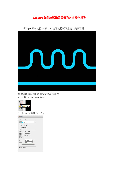
Allegro如何绕弧线的等长和对内操作指导Allegro不仅支持45度,90度还支持弧形走线,类似下图当需要绕弧线等长的时候可以如下操作1.选择Delay Tune命令2.Corners选择FullArc3.选中需要绕的线就会出现弧线This section is describe what the function allegro have ,helpfully could let user know more about allegroAllegro Design and Analysis includes design authoringPCB layout and Library and Design Data ManagementWith. It can ensure the end-to-end design of PCB with high quality and efficiencyRealize smooth data transfer between tools, shorten PCB design cycle, and shorten productMarket time1. Design authoringProvide a flexible logic constraint driven flow, management design rules, network hierarchy,Bus and differential pair.1.1.1 Main features and functionsThrough hierarchical and design "derivation" function, improve the original of complex designMap editing efficiency.Powerful CIS helps users quickly determine part selection and accelerate design flowAnd reduce project cost.1.2.1 Main featuresSchematic designers and PCB design engineers can work in parallel. Advanced design efficiency improves functions, such as copying the previous schematic design Select multiplexing with or by page. Seamless integration into pre simulation and signal analysis.1.2.2 Main FunctionsProvide schematic diagram and HDL/Verilog design input.Assign and manage high-speed design rules.Support netclasses, buses, extension networks and differential pairs. Powerful library creation and management functions.Allows synchronization of logical and physical designs.Realize multi-user parallel development and version control.Pre integration simulation and signal analysis.Support customizable user interface and enterprise customization development.1.3 o Allegro n Design Publisher1.3.1 Main Features and FunctionsAllows you to share designs with others using PDF files.The entire design is represented in a single, compact PDF format. Improve design readability.Provide content control - users can select the content to be published.1.4 Allegro A FPGA m System Planner1 1.4.1 Main features and functionsComplete and scalable FPGA/PCB collaborative design technology for ideal "Design and correct "pin assignment.Scalable FPGA/PCB protocol from OrCAD Capture to Allegro GXLSame as the design solution.Shorten the optimization pin allocation time and accelerate the PCB design cycle.2. B PCB layoutIt provides expandable and easy to use PCB design (including RFPCB) Then drive PCB design solution. It also includes innovative new automatic deliveryMutual technology can effectively improve the wiring of high-speed interfaces; Apply EDMD (IDX) mode, which makes ECAD/MCAD work smoothly; Execute modern industry standard IPC-2581,Ensure that the design data is simply and high-quality transferred to the downstream link.2.1.1 Main featuresSpeed up the design process from layout, wiring to manufacturing. Including powerful functions, such as design zoning, RF design functions and global design rules Stroke.It can improve productivity and help engineers to quickly move up to mass production* g- M4 G8 |6 }9 k7 G2.1.2 Main FunctionsProvide scalable full function PCB design solutions.Enable constraint driven design processes to reduce design iterations. Integrated DesignTrueDFM technology provides real-time DFM inspection. Provide a single, consistent context for management.Minimize design iterations and reduce overall Flex and rigid flexible designCost, and has advanced rigid and flexible design functions.Realize dynamic concurrent team design capability, shorten design cycle,and greatly reduceTime spent in routing, winding and optimization.Provide integrated RF/analog design and mixed signal design environment. Provides interactive layout and component placement.Provide design partitions for large distributed development teams. Realize real-time, interactive push editing of routing.It is allowed to use dynamic copper sheet technology to edit and update in real time.Manage netscheduling, timing, crosstalk, routing by designated layer and area Bundle.Provide proven PCB routing technology for automatic routing.Realize hierarchical route planning and accelerate the completion of design.Shorten interconnect planning and cabling time for high-speed interface intensive design.Provide a comprehensive, powerful and easy-to-use tool suite to help designersEfficient and successful manufacturing switch: DFM Checker is aimed at the company/manufacturerReview the specific rules of manufacturing partners; Used to reduce manufacturing and assembly documentsThe document editing time of the file can reach 70%; The panel editor will assemble the panel designThe intention is communicated to the manufacturing partners; Output design data in various manufacturing formats.3. y Library d and n Design a Data ManagementFor cost-effective projects that need to be delivered on time, it is easy to obtainCurrent component information and design data are critical. library and designData management is a collaborative control of the company's internal cooperation and design processAdvanced functions are provided. As the design cycle shortens and the complexity increases, youThere must be a design approach that increases predictability and accelerates design turnaround.3.1.1 Main featuresReduce time and optimize library development related resources. Improve the precision in the process of parts manufacturing. Q9 b3.1.2 Main functionsReduce time and optimize library development and validation through integrated creation and validation processes Certification related resources.A simple method to develop devices with large pin count can shortenthe time from a few days to A few minutes.Powerful graphic editor supports custom shape and spreadsheet import forSchematic symbols are created to ensure the reliability and integrity of data.Supports the import of part information from general industry formats, allowing rapid creation and Update part information.Common library development environment supporting schematic tools from different suppliers, including Mentor Graphics Design Architect and Mentor Graphics Viewdraw。
allegro等长设置总结.doc
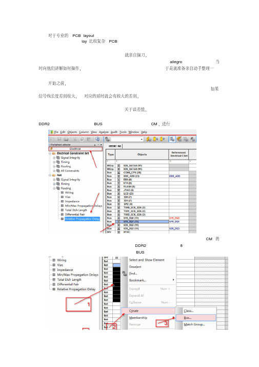
对于专业的PCB layoutlay比较复杂PCB就亲自操刀,allegro当时向他们讲解如何操作,于是就准备亲自动手整理一开始之前,如果信号线长度差别较大,对应的延时就会有较大的差别,关于误差值,DDR2BUS CM,进行CM的DDR28BUS选中信号---右键选择create---BUSBUS OK BUSBUSBUSBUS BUS1.BUS SiXplorer…2.3.1Rel Prop Delayrule name From和ToFrom和To.Delta和Tolerance就是误差长度,如0mil和25mil,50mil,信号线和参考基准信号线25milAdd—Apply—OK.CM File---update CM.constraint manager.1.回到CM rule nameBUS name的MGrp2.MGrp的name,右键analyzelength,升序or降序,1.delay tune2.1.BUS中的信号的模型不一样,如MGrp2.BUS rule name建的rule name MGrp 关于XnetXnetXnet1.Analyze>SI/EMI Sim>Model…DC net,直接YesModel2.model Detype value/refdes3.点选create mode…4.okModenameCircuit typeSingle pins116pin,就连着,接着215相当于另一个电阻…pin number之间用空格隔开,如1和1616和22和15之间…net的property Member of XNet:…XnetPin Pair1.在BUS create---pin pairok net pin pair netppr pin pair2.match group MGrp BUS中所有的ppr,右键create...membership3.MGrp就ok4.set target有时,Pin pin type,pin type,pin pair1,Edit>Properties…2,在Find栏位中勾选Pin3,在PCB中选中需要修改Pin Type的Pin4,Edited by Kevin2013/11/10。
Allegro线宽、间距、等长、差分

A llegro 中的约束规则设置Allegrophan 刚好五个字w w w .pc b b b s .c o m修订记录日期版本描述作者2008-12V1.0初版,学完的总结。
适用于Cadence 15.5版本。
Allegrophan 2009-09-08V1.1小改,修改部分措辞Allegrophan 2009-10-14V1.2小改,更正、修改几个错漏之处。
添加一些说明性文字。
感谢群里的佳猪、梦姑娘等朋友的指正!Allegrophanw w w .p c b b b s .c o m目录一:Physical (Line/vias )rule 物理特性(线宽和过孔)约束设置:.............41)“Set values”设置约束特征值....................................................................52)“Attach property ”绑定约束.....................................................................63)“Assignment table ”约束规则分配........................................................8二“Spacing rule”间距约束设置...........................................................................91)“Set values ”设置约束特征值................................................................92)“Attach property ”绑定约束.................................................................103)“Assignment table ”约束规则分配......................................................11三Constraint areas 区域约束设置......................................................................12四Allegro 中走线长度的设置............................................................................131)差分线等长设置......................................................................................132)一组Net 等长..........................................................................................163)XNet 等长................................................................................................17w w w .p c b b b s .c o m线宽、线距、区域的约束主要在“Constraints Sys ”中设置,点击“Setup/Constraints ”或点击图标打开“Constraints Sys ”窗口,如下:“Constraints Sys ”窗口分两个级别,第一级别有两类:Standard design rules 和Exte Extended nded design rules 。
allegro设置差分线和等长的方法
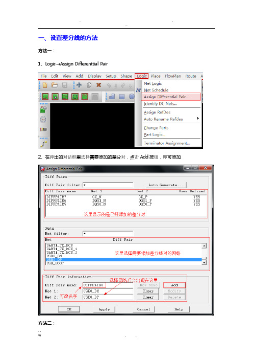
一、设置差分线的方法方法一:1、Logic→Assign Differenttial Pair2、在弹出的对话框里选择需要添加的差分对,点击Add按钮,即可添加方法二:1、Setup→Constraints→Electrical2、选择Net,然后在Objects→Create→Differenttial Pair3、在弹出的对话框里选择需要添加的差分对,点击Create按钮,即可添加设置完差分线对后,需要设置其约束规则,方法如下:1、初始默认的有一个DEFAULT规则,右击DEFAUlT,选择Create→Physical CSet2、弹出一下对话框,在Physical CSet栏写上规则名称,建议根据差分线的阻抗描写,点击OK,这里已经写好,规则名称为:DIFF100,就可以看到多了一行PCS3、设立好规则后就可以在这项规则里设置线宽间距等参数了4、在Net一栏看到有已经设好的差分线,在Referenced physical C Set选项下选择刚刚设好的规则DIFF100*规则设置中各个项目的含义*Line Width(设置基本走线宽度)Min:最小线宽Max:最大线宽,写0相当于无限大Neck(neck模式,一般在间距很小的时候用到)Min Width:最小线宽Max Length:最大线长Differential Pair(差分线设置,单端线可不写)Min Line Spacing:差分对的最小线间距Primary Gap:差分对理想线间距Neck Gap:差分对最小允许线间距(+)T olerance:差分线允许的误差+(-)Tolerance:差分线允许的误差-Vias(过孔选择)BB Via Stagger(设置埋/盲孔的过孔间距)Min:最小间距Max:最大间距AllowPad-Pad Connect:/ Etch:/Ts:/示意图:二、设置等长1、进入规则设置页面Electrical→Net→Routing→Relative Propagation Delay2、选中需要设置等长的网络,右击,选择Create→Match Group3、更改组名称4、设置好后,会显示MGrp,如下图。