清华大学数字大规模集成电路05-CMOS反相器
数字集成电路实验-反相器实验报告
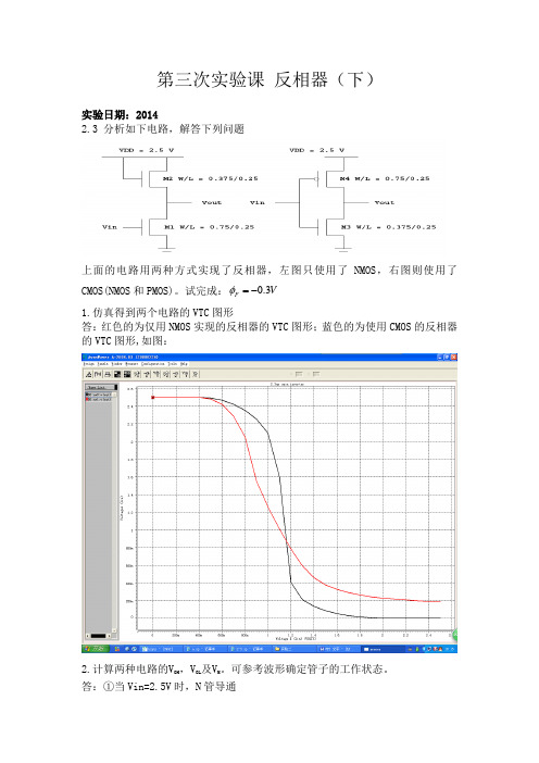
第三次实验课 反相器(下)实验日期:20142.3 分析如下电路,解答下列问题上面的电路用两种方式实现了反相器,左图只使用了NMOS ,右图则使用了CMOS(NMOS 和PMOS)。
试完成:V F 3.0-=φ1.仿真得到两个电路的VTC 图形答:红色的为仅用NMOS 实现的反相器的VTC 图形;蓝色的为使用CMOS 的反相器的VTC 图形,如图:2.计算两种电路的V OH ,V OL 及V M 。
可参考波形确定管子的工作状态。
答:①当Vin=2.5V 时,N 管导通有在体偏置条件下阀值电压公式:)22(0F SB F T T V V V φφγ-+-+=()()()⎥⎦⎤⎢⎣⎡--=⎥⎦⎤⎢⎣⎡--=⎥⎦⎤⎢⎣⎡--=22220'2011'222'OL OL T in n DS DS T GS M M n d DSAT DSAT T DD M M n DSAT V V V V L W k V V V V L W k I V V V V L W k I (M2速度饱和)将下列数据代人VV V A k V V V D SAT n F T 63.0,/10115,3.0,43.026'0=⨯=-==-φ25.075.0,25.0375.01122==M M M M L W L W解得: V V OL 2875.0=当Vin=0V 时,N 管截止,Vout=OH V =2.5V求解M V :当out in V V =时,由于GS DS V V =,M1工作在饱和区此时流过M1(速度饱和)的电流为:()⎥⎥⎦⎤⎢⎢⎣⎡--=22011'1DSAT DSAT T in M M n DSAT V V V V L W k I (1) 流过M2的电流为(速度饱和)()⎥⎥⎦⎤⎢⎢⎣⎡---=2222'2DSAT DSAT T out DD M M n DSAT V V V V V L W k I (2) )22(0F SB F T T V V V φφγ-+-+=(3)M out in SB V V V V ===联立方程解得M V =1.017V②对于CMOS 器件当Vin=0时,V V V out O H 5.2==当Vin=2.5时,V V V out O L 0==求解M V :当out in V V =时,由于GS DS V V =,NMOS 与PMOS 工作在饱和区由于T M D SAT V V V -<,此时已经发生了速度饱和(参考波形)代入,联立解得:将下列数据V V V V V V V V V A k V A k L W k k L W k k V k V k r r V V V r V V V V V V V V k V V V V k DSATp DSATn Tp Tn p n pp p p nn n n DSATnn DSATpp DSAT TP DD DSAT Tn M DSATp Tp DD M DSATp p DSATn Tn M DSATn n 1,63.04.0,43.0,/1030,/101151)2/()2/(0)2/()2/(26'26'''-==-==⨯-=⨯====+++++==---+----M V =1.132315968V3.哪一种结构的反相器的功能性更好,为什么?(噪声容限,再生性,过渡区增益)答:CMOS 反相器更好。
数字集成电路反相器

一、实验目的:
1、熟悉T-spice的使用,并且熟练掌握。
2、仿真出反相器的输出曲线,并观察它的特性。
二、实验原理:
CMOS反相器由一个P沟道增强型MOS管和一个N沟道增强型MOS管串联组成。
通常P 沟道管作为负载管,N沟道管作为输入管。
两个MOS管的开启电压VGS(th)P<0,VGS(th)N >0,通常为了保证正常工作,要求VDD>|VGS(th)P|+VGS(th)N。
若输入vI为低电平(如0V),则负载管导通,输入管截止,输出电压接近VDD。
若输入vI为高电平(如VDD),则输入管导通,负载管截止,输出电压接近0V。
三、实验步骤:
1、画出反相器的仿真图
实验小结:
通过这次Hspice仿真反相器的上机实验,我收获颇多。
第一、我更加熟悉了Hspice 仿真环境的使用,对T-spice更加的熟练。
这将对我以后再做其它实验奠定了良好的基础。
第二、以前只在课堂上听老师讲授那些反相器的原理和输出曲线等,但自己的意识当中对反相器的工作还是很疑惑,在做完这个仿真实验后,才恍然大悟,觉得反相器原来就是这么回事。
第三、反相器是我们学习数字集成电路的桥梁,我们后续将会用它进行许多的设计,所以这次实验的重要度是很高的。
我非常的重视这次实验。
MOS集成电路--CMOS反相器电路仿真及版图设计
MOS集成电路--CMOS反相器电路仿真及版图设计MOS管集成电路设计题⽬:CMOS反相器电路仿真及版图设计姓名:潘朝云学号:20111060198专业:通信⼯程指导⽼师:梁⽵关2014年6⽉1⽇摘要本⽂介绍了集成电路设计的相关思路、电路的实现、SPICE电路模拟软件和LASI7集成电路版图设计的相关⽤法。
主要讲述CMOS反相器的设计⽬的、设计的思路、以及设计的过程,⽤SPICE电路设计软件来实现对反相器的设计和仿真。
集成电路反相器的实现⽤到NMOS和PMOS各⼀个,⽤LASI7实现了其版图的设计。
关键字:集成电路CMOS反相器LT SPICE LASI7⽬录引⾔ ....................................................................................................................................... - 2 -⼀、概述 ............................................................................................................................... - 2 -1.1MOS集成电路简介.................................................................................................... - 2 -1.2MOS集成电路分类.................................................................................................... - 2 -1.3MOS集成电路的优点................................................................................................ - 3 -⼆、LTspice电路仿真 .......................................................................................................... - 3 -2.1SPICE简介 ................................................................................................................... - 3 -2.2CMOS反相器LT SPICE仿真过程 ..................................................................... - 3 -2.2.1实现⽅案 .............................................................................................................. - 3 -2.2.2 LTspice电路仿真结果 ...................................................................................... - 5 -三、LASI版图设计 ............................................................................................................... - 5 -3.1LASI软件简介........................................................................................................ - 5 -3.2版图设计原理......................................................................................................... - 6 -3.3LASI的版图设计.................................................................................................... - 6 -四、实验结果分析 ............................................................................................................... - 8 -五、结束语 ........................................................................................................................... - 8 -参考⽂献 ............................................................................................................................... - 8 -引⾔CMOS技术⾃⾝的巨⼤潜⼒是IC⾼速持续发展的基础。
CMOS反相器的电传输特性

★CMOS反相器的电压传输特性★CMOS反相器的输入输出特性★TTL与CMOS集成电路性能比较7.1 MOS集成逻辑门MOS集成逻辑门是由MOS场效应晶体管组成的数字集成电路MOS集成逻辑门:制作工艺简单,成本低,输入阻抗极高,功耗低,集成度高工作电源允许变化范围大,抗干扰性能较好能与大多数的TTL逻辑电路兼容。
在LSI(大规模集成电路)及VLSI超大规模集成电路的制作上已经超过TTL,并占据优势。
场效应晶体管是电压控制型器件与双极性晶体管相比较具有许多优点。
MOS集成逻辑门分P沟道增强(称PMOS)N沟道增强(称NMOS)和互补MOS(称CMOS)三种。
PMOS由于开关速度低,电源电压高而且是负电源,不便与TTL集成逻辑门衔接,现以很少用;NMOS克服了PMOS的许多问题,但速度低的问题始终限制了其发展;CMOS充分表现了MOS技术的突出优点,成为LSI及VLSI集成电路的主流产品。
7.2 CMOS反相器的工作原理1.电路结构负载管P沟道结构的增强型场效应管N沟道结构的增强型场效应管驱动管这种由T1,T2共同组成的互补对称型的场效应管集成电路称为CMOS反相器。
2.电路工作原理uI0V时,uGSN0V T2截止截止导通uGSP -10V T1导通0 -10输出vO为高电平; 1 0 0 10uI 10V时,uGSN10V 此时T2导通0 10uGSP 0V T1截止导通截止输出vO为低电平。
输入和输出之间为反相关系,实现非门逻辑功能7.3 CMOS传输门和双向模拟开关1.电路结构CMOS传输门双向模拟开关2.工作原理:PMOS管PMOS管设T1管和T2管的开启电压UGSthNUGSthPUGSth VDD≥2 UGSth 控制信号C的高电平为VDD,低电平为0V。
(1)当 C 0 C 0 传输门不传输信号。
因为T1管和T2管均处于截止状态相当于电路是断开的。
(2)当 C 0 C 0 T1管和T2管均导通,即传输门导通,uouI uI可以是0V到VDD的任意电压。
集成电路课程设计--cmos反相器的电路设计及版图设计

目录摘要 (3)绪论 (5)1软件介绍及电路原理 (6)1.1软件介绍 (6)1.2电路原理 (6)2原理图绘制 (8)3电路仿真 (10)3.1瞬态仿真 (10)3.2直流仿真 (11)4版图设计及验证 (12)4.1绘制反相器版图的前期设置 (12)4.2绘制反相器版图 (13)4.3 DRC验证 (15)结束语 (17)参考文献 (18)摘要CMOS技术自身的巨大发展潜力是IC高速持续发展的基础。
集成电路制造水平发展到深亚微米工艺阶段,CMOS的低功耗、高速度和高集成度得到了充分的体现。
本文将简单的介绍基于ORCAD和L-EDIT的CMOS反相器的电路仿真和版图设计,通过CMOS反相器的电路设计及版图设计过程,我们将了解并熟悉集成电路CAD的一种基本方法和操作过程。
关键词:CMOS反相器ORCAD L-EDIT版图设计AbstractThe huge development potential of CMOS technology itself is the foundation of sustainable development of IC high speed. The manufacturing level of development of the integrated circuit to the deep sub micron technology, CMOS low power consumption, high speed and high integration have been fully reflected. In this paper, the circuit simulation and layout design of ORCAD and L-EDIT CMOS inverter based on simple introduction, through the circuit design and layout design process of CMOS inverter, we will understand and a basic method and operation process, familiar with IC CAD.Keywords: CMOS inverter layout ORCAD L-EDIT绪论20世纪是IC迅速发展的时代。
数字集成电路--电路、系统与设计(第二版)课后练习题 第五章 CMOS反相器
C H A P T E R5T H E C M O S I N V E R T E R Quantification of integrity,performance,and energy metrics of an inverterOptimization of an inverter design5.1Exercises and Design Problems5.2The Static CMOS Inverter—An IntuitivePerspective5.3Evaluating the Robustness of the CMOSInverter:The Static Behavior5.3.1Switching Threshold5.3.2Noise Margins5.3.3Robustness Revisited5.4Performance of CMOS Inverter:The DynamicBehavior5.4.1Computing the Capacitances5.4.2Propagation Delay:First-OrderAnalysis5.4.3Propagation Delay from a DesignPerspective5.5Power,Energy,and Energy-Delay5.5.1Dynamic Power Consumption5.5.2Static Consumption5.5.3Putting It All Together5.5.4Analyzing Power Consumption UsingSPICE5.6Perspective:Technology Scaling and itsImpact on the Inverter Metrics180Section 5.1Exercises and Design Problems 1815.1Exercises and Design Problems1.[M,SPICE,3.3.2]The layout of a static CMOS inverter is given in Figure 5.1.(λ=0.125µm).a.Determine the sizes of the NMOS and PMOS transistors.b.Plot the VTC (using HSPICE)and derive its parameters (V OH ,V OL ,V M ,V IH ,and V IL ).c.Is the VTC affected when the output of the gates is connected to the inputs of 4similargates?.d.Resize the inverter to achieve a switching threshold of approximately 0.75V .Do not lay-out the new inverter,use HSPICE for your simulations.How are the noise margins affected by this modification?2.Figure 5.2shows a piecewise linear approximation for the VTC.The transition region isapproximated by a straight line with a slope equal to the inverter gain at V M .The intersectionof this line with the V OH and the V OL lines defines V IH and V IL .a.The noise margins of a CMOS inverter are highly dependent on the sizing ratio,r =k p /k n ,of the NMOS and PMOS e HSPICE with V Tn =|V Tp |to determine the valueof r that results in equal noise margins?Give a qualitative explanation.b.Section 5.3.2of the text uses this piecewise linear approximation to derive simplifiedexpressions for NM H and NM L in terms of the inverter gain.The derivation of the gain isbased on the assumption that both the NMOS and the PMOS devices are velocity saturatedat V M .For what range of r is this assumption valid?What is the resulting range of V M ?c.Derive expressions for the inverter gain at V M for the cases when the sizing ratio is justabove and just below the limits of the range where both devices are velocity saturated.What are the operating regions of the NMOS and the PMOS for each case?Consider theeffect of channel-length modulation by using the following expression for the small-signalresistance in the saturation region:r o,sat =1/(λI D ).Figure 5.1CMOS inverter layout.InOutGND V DD =2.5V.Poly Metal1NMOSPMOSPolyMetal12λ182THE CMOS INVERTER Chapter 53.[M,SPICE,3.3.2]Figure 5.3shows an NMOS inverter with resistive load.a.Qualitatively discuss why this circuit behaves as an inverter.b.Find V OH and V OL calculate V IH and V IL .c.Find NM L and NM H ,and plot the VTC using HSPICE.d.Compute the average power dissipation for:(i)V in =0V and (ii)V in =2.5Ve HSPICE to sketch the VTCs for R L =37k,75k,and 150k on a single graph.ment on the relationship between the critical VTC voltages (i.e.,V OL ,V OH ,V IL ,V IH )and the load resistance,R L .g.Do high or low impedance loads seem to produce more ideal inverter characteristics?4.[E,None,3.3.3]For the inverter of Figure 5.3and an output load of 3pF:a.Calculate t plh ,t phl ,and t p .b.Are the rising and falling delays equal?Why or why not?pute the static and dynamic power dissipation assuming the gate is clocked as fast as possible.5.The next figure shows two implementations of MOS inverters.The first inverter uses onlyNMOS transistors.V OH V OL inV outFigure 5.2A different approach to derive V IL and V IH .V outV in M 1W/L =1.5/0.5+2.5VFigure 5.3Resistive-load inverterR L =75k ΩSection 5.1Exercises and Design Problems183a.Calculate V OH ,V OL ,V M for each case.e HSPICE to obtain the two VTCs.You must assume certain values for the source/drain areas and perimeters since there is no layout.For our scalable CMOS process,λ =0.125μm,and the source/drain extensions are 5λfor the PMOS;for the NMOS the source/drain contact regions are 5λx5λ.c.Find V IH ,V IL ,NM L and NM H for each inverter and comment on the results.How can you increase the noise margins and reduce the undefined region?ment on the differences in the VTCs,robustness and regeneration of each inverter.6.Consider the following NMOS inverter.Assume that the bulk terminals of all NMOS deviceare connected to GND.Assume that the input IN has a 0V to 2.5V swing.a.Set up the equation(s)to compute the voltage on node x .Assume γ=0.5.b.What are the modes of operation of device M2?Assume γ=0.c.What is the value on the output node OUT for the case when IN =0V?Assume γ=0.d.Assuming γ=0,derive an expression for the switching threshold (V M )of the inverter.Recall that the switching threshold is the point where V IN =V OUT .Assume that the devicesizes for M1,M2and M3are (W/L)1,(W/L)2,and (W/L)3respectively.What are the limitson the switching threshold?For this,consider two cases:i)(W/L)1>>(W/L)2V DD =2.5V V IN V OUTV DD =2.5V V IN V OUT M 2M 1M 4M 3W/L=0.375/0.25W/L=0.75/0.25W/L=0.375/0.25W/L=0.75/0.25Figure 5.4Inverter ImplementationsV DD =2.5V OUTM1IN M2M3V DD =2.5Vx184THE CMOS INVERTER Chapter 5ii)(W/L)2>>(W/L)17.Consider the circuit in Figure 5.5.Device M1is a standard NMOS device.Device M2has allthe same properties as M1,except that its device threshold voltage is negative and has a valueof -0.4V.Assume that all the current equations and inequality equations (to determine themode of operation)for the depletion device M2are the same as a regular NMOS.Assume thatthe input IN has a 0V to 2.5V swing.a.Device M2has its gate terminal connected to its source terminal.If V IN =0V ,what is the output voltage?In steady state,what is the mode of operation of device M2for this input?pute the output voltage for V IN =2.5V .You may assume that V OUT is small to simplify your calculation.In steady state,what is the mode of operation of device M2for this input?c.Assuming Pr (IN =0)=0.3,what is the static power dissipation of this circuit?8.[M,None,3.3.3]An NMOS transistor is used to charge a large capacitor,as shown in Figure5.6.a.Determine the t pLH of this circuit,assuming an ideal step from 0to 2.5V at the input node.b.Assume that a resistor R S of 5k Ωis used to discharge the capacitance to ground.Deter-mine t pHL .c.Determine how much energy is taken from the supply during the charging of the capacitor.How much of this is dissipated in M1.How much is dissipated in the pull-down resistanceduring discharge?How does this change when R S is reduced to 1k Ω.d.The NMOS transistor is replaced by a PMOS device,sized so that k p is equal to the k n ofthe original NMOS.Will the resulting structure be faster?Explain why or why not.9.The circuit in Figure 5.7is known as the source follower configuration.It achieves a DC levelshift between the input and the output.The value of this shift is determined by the current I 0.Assume x d =0,γ=0.4,2|φf |=0.6V ,V T 0=0.43V ,k n ’=115μA/V 2and λ=0.V DD =2.5VOUTM1(4μm/1μm)IN M2(2μm/1μm),V Tn =-0.4VFigure 5.5A depletion load NMOSinverterV DD =2.5VOutFigure 5.6Circuit diagram with annotated W/L ratios=5pFSection 5.1Exercises and Design Problems 185a.Suppose we want the nominal level shift between V i and V o to be 0.6V in the circuit in Figure 5.7(a).Neglecting the backgate effect,calculate the width of M2to provide this level shift (Hint:first relate V i to V o in terms of I o ).b.Now assume that an ideal current source replaces M2(Figure 5.7(b)).The NMOS transis-tor M1experiences a shift in V T due to the backgate effect.Find V T as a function of V o for V o ranging from 0to 2.5V with 0.5V intervals.Plot V T vs.V oc.Plot V o vs.V i as V o varies from 0to 2.5V with 0.5V intervals.Plot two curves:one neglecting the body effect and one accounting for it.How does the body effect influence the operation of the level converter?d.At V o (with body effect)=2.5V,find V o (ideal)and thus determine the maximum error introduced by the body effect.10.For this problem assume:V DD =2.5V ,W P /L =1.25/0.25,W N /L =0.375/0.25,L =L eff =0.25μm (i.e.x d =0μm),C L =C inv-gate ,k n ’=115μA/V 2,k p ’=-30μA/V 2,V tn0=|V tp0|=0.4V,λ =0V -1, γ=0.4,2|φf |=0.6V ,and t ox =e the HSPICE model parameters for parasitic capacitance given below (i.e.C gd0,C j ,C jsw ),and assume that V SB =0V for all problems except part (e).Figure 5.7NMOS source follower configuration V DD =2.5V V iV oV DD =2.5VV i V oV bias =(a)(b)I o1um/0.25um M1186THE CMOS INVERTER Chapter 5##Parasitic Capacitance Parameters (F/m)##NMOS:CGDO=3.11x10-10,CGSO=3.11x10-10,CJ=2.02x10-3,CJSW=2.75x10-10PMOS:CGDO=2.68x10-10,CGSO=2.68x10-10,CJ=1.93x10-3,CJSW=2.23x10-10a.What is the V m for this inverter?b.What is the effective load capacitance C Leff of this inverter?(include parasitic capacitance,refer to the text for K eq and m .)Hint:You must assume certain values for the source/drain areas and perimeters since there is no layout.For our scalable CMOS process,λ =0.125μm,and the source/drain extensions are 5λfor the PMOS;for the NMOS the source/drain contact regions are 5λx5λ.c.Calculate t PHL ,t PLH assuming the result of (b)is ‘C Leff =6.5fF’.(Assume an ideal step input,i.e.t rise =t fall =0.Do this part by computing the average current used to charge/dis-charge C Leff .)d.Find (W p /W n )such that t PHL =t PLH .e.Suppose we increase the width of the transistors to reduce the t PHL ,t PLH .Do we get a pro-portional decrease in the delay times?Justify your answer.f.Suppose V SB =1V,what is the value of V tn ,V tp ,V m ?How does this qualitatively affect C Leff ?ing Hspice answer the following questions.a.Simulate the circuit in Problem 10and measure t P and the average power for input V in :pulse(0V DD 5n 0.1n 0.1n 9n 20n),as V DD varies from 1V -2.5V with a 0.25V interval.[t P =(t PHL +t PLH )/2].Using this data,plot ‘t P vs.V DD ’,and ‘Power vs.V DD ’.Specify AS,AD,PS,PD in your spice deck,and manually add C L =6.5fF.Set V SB =0Vfor this problem.b.For Vdd equal to 2.5V determine the maximum fan-out of identical inverters this gate candrive before its delay becomes larger than 2ns.c.Simulate the same circuit for a set of ‘pulse’inputs with rise and fall times of t in_rise,fall =1ns,2ns,5ns,10ns,20ns.For each input,measure (1)the rise and fall times t out_rise andV DD =2.5VV IN V OUTC L =C inv-gateL =L P =L N =0.25μmV SB-+(W p /W n =1.25/0.375)Figure 5.8CMOS inverter with capacitiveSection 5.1Exercises and Design Problems 187t out_fall of the inverter output,(2)the total energy lost E total ,and (3)the energy lost due to short circuit current E short .Using this data,prepare a plot of (1)(t out_rise +t out_fall )/2vs.t in_rise,fall ,(2)E total vs.t in_rise,fall ,(3)E short vs.t in_rise,fall and (4)E short /E total vs.t in_rise,fall.d.Provide simple explanations for:(i)Why the slope for (1)is less than 1?(ii)Why E short increases with t in_rise,fall ?(iii)Why E total increases with t in_rise,fall ?12.Consider the low swing driver of Figure 5.9:a.What is the voltage swing on the output node (V out )?Assume γ=0.b.Estimate (i)the energy drawn from the supply and (ii)energy dissipated for a 0V to 2.5V transition at the input.Assume that the rise and fall times at the input are 0.Repeat the analysis for a 2.5V to 0V transition at the input.pute t pLH (i.e.the time to transition from V OL to (V OH +V OL )/2).Assume the input rise time to be 0.V OL is the output voltage with the input at 0V and V OH is the output volt-age with the input at 2.5V .pute V OH taking into account body effect.Assume γ =0.5V 1/2for both NMOS and PMOS.13.Consider the following low swing driver consisting of NMOS devices M1and M2.Assumean NWELL implementation.Assume that the inputs IN and IN have a 0V to 2.5V swing andthat V IN =0V when V IN =2.5V and vice-versa.Also assume that there is no skew between INand IN (i.e.,the inverter delay to derive IN from IN is zero).a.What voltage is the bulk terminal of M2connected to?V in V out V DD =2.5V W L 3μm 0.25μm =p 2.5V0V C L =100fFW L 1.5μm 0.25μm=n Figure 5.9Low Swing DriverV LOW =0.5VOutM1ININ M225μm/0.25μm 25μm/0.25μmC L =1pFFigure 5.10Low Swing Driver188THE CMOS INVERTER Chapter 5b.What is the voltage swing on the output node as the inputs swing from 0V to 2.5V .Showthe low value and the high value.c.Assume that the inputs IN and IN have zero rise and fall times.Assume a zero skewbetween IN and IN.Determine the low to high propagation delay for charging the outputnode measured from the the 50%point of the input to the 50%point of the output.Assumethat the total load capacitance is 1pF,including the transistor parasitics.d.Assume that,instead of the 1pF load,the low swing driver drives a non-linear capacitor,whose capacitance vs.voltage is plotted pute the energy drawn from the lowsupply for charging up the load capacitor.Ignore the parasitic capacitance of the driver cir-cuit itself.14.The inverter below operates with V DD =0.4V and is composed of |V t |=0.5V devices.Thedevices have identical I 0and n.a.Calculate the switching threshold (V M )of this inverter.b.Calculate V IL and V IH of the inverter.15.Sizing a chain of inverters.a.In order to drive a large capacitance (C L =20pF)from a minimum size gate (with inputcapacitance C i =10fF),you decide to introduce a two-staged buffer as shown in Figure5.12.Assume that the propagation delay of a minimum size inverter is 70ps.Also assumeV DD =0.4VV IN V OUTFigure 5.11Inverter in Weak Inversion RegimeSection 5.1Exercises and Design Problems 189that the input capacitance of a gate is proportional to its size.Determine the sizing of thetwo additional buffer stages that will minimize the propagation delay.b.If you could add any number of stages to achieve the minimum delay,how many stages would you insert?What is the propagation delay in this case?c.Describe the advantages and disadvantages of the methods shown in (a)and (b).d.Determine a closed form expression for the power consumption in the circuit.Consider only gate capacitances in your analysis.What is the power consumption for a supply volt-age of 2.5V and an activity factor of 1?16.[M,None,3.3.5]Consider scaling a CMOS technology by S >1.In order to maintain compat-ibility with existing system components,you decide to use constant voltage scaling.a.In traditional constant voltage scaling,transistor widths scale inversely with S,W ∝1/S.To avoid the power increases associated with constant voltage scaling,however,youdecide to change the scaling factor for W .What should this new scaling factor be to main-tain approximately constant power.Assume long-channel devices (i.e.,neglect velocitysaturation).b.How does delay scale under this new methodology?c.Assuming short-channel devices (i.e.,velocity saturation),how would transistor widthshave to scale to maintain the constant power requirement?1InAdded Buffer StageOUTC L =20pF C i =10fF‘1’is the minimum size inverter.??Figure 5.12Buffer insertion for driving large loads.190THE CMOS INVERTER Chapter5DESIGN PROBLEMUsing the0.25μm CMOS introduced in Chapter2,design a static CMOSinverter that meets the following requirements:1.Matched pull-up and pull-down times(i.e.,t pHL=t pLH).2.t p=5nsec(±0.1nsec).The load capacitance connected to the output is equal to4pF.Notice that thiscapacitance is substantially larger than the internal capacitances of the gate.Determine the W and L of the transistors.To reduce the parasitics,useminimal lengths(L=0.25μm)for all transistors.Verify and optimize the designusing SPICE after proposing a first design using manual -pute also the energy consumed per transition.If you have a layout editor(suchas MAGIC)available,perform the physical design,extract the real circuitparameters,and compare the simulated results with the ones obtained earlier.。
数字集成电路设计第5章cmos反相器教材
线性化
Ceq = Keq Cj0
高到低 低到高 Keqbp Keqsw Keqbp Keqsw NMOS 0.57 0.61 0.79 0.81
PMOS
0.79
0.86
0.59
0.7
2019/4/17
33
一个0.25umCMOS反相器的电容
2019/4/17
27
即使电源电压很低时,晶体管仍能导通,仍然 具有反相器的特性,因为亚阈值电流足以使该门在 低电平和高电平之间切换,并提供足够的增益从而 得到可接受的VTC。
但使得门的特性变的很差。VOL和VOH不再等于 电源的两个电平,并且过渡区的增益接近1。 为了能得到足够的增益以用于数字电路,必须使 电源为热电势的两倍,否则就只能降低热电势,即 降低环境温度,冷却该电路
能量效率:由能耗和功耗决定。
2019/4/17 2
5.2静态CMOS反相器—综述
VDD
Vin CL
Vout
把MOS晶体管当成简单的开关模型。即晶体管只不过是一个具有无限关断电阻 和有限导通电阻的开关。(VGS与VT 的关系所决定)
2019/4/17 3
VDD
VDD
VDD
0 0
CL
CL
VDD CL
2019/4/17
7
IDn
IDSp = -IDSn VGSn = Vin ; VGSp = Vin - VDD VDSn = Vout ; VDSp = Vout - VDD
Vout
Vin = 0 Vin = 1.5
Vin = 0 Vin = 1.5
VGSp = -1 VGSp = -2.5
Vin = VDD + VGSp IDn = -IDp
清华大学《数字集成电路设计》周润德 第5章 CMOS反相器
第五章 CMOS 反相器 第一节 对逻辑门的基本要求(1)鲁棒性(用静态或稳态行为来表示)静态特性常常用电压传输特性(VTC)来表示(即输出与输入的关系), 传输特性上具有一些重要的特征点。
逻辑门的功能会因制造过程的差异而偏离设计的期望值。
V(y) 电压传输特性(直流工作特性)VOH fV(y)=V(x)VM开关阈值VOL VOL VOHVOH = f(VOL) VOL = f(VOH) VM = f(VM)V(x)额定电平2004-9-29 清华大学微电子所《数字大规模集成电路》 周润德 第5章第1页(2)噪声容限:芯片内外的噪声会使电路的响应偏离设计的期望值 (电感、电容耦合,电源与地线的噪声)。
一个门对于噪声的敏感程度由噪声容限表示。
可靠性―数字集成电路中的噪声v(t) i(t)V DD电感耦合电容耦合电源线与地线噪声噪声来源: (1)串扰 (2)电源与地线噪声 (3)干扰 (4)失调 应当区分: (1)固定噪声源 (2)比例噪声源 浮空节点比由低阻抗电压源驱动的节点更易受干扰 设计时总的噪声容限分配给所预见的噪声源2004-9-29 清华大学微电子所《数字大规模集成电路》 周润德 第5章第2页噪声容限(Noise Margin)V“1” V OH V IHout OH 斜率 = -1V不确定区 斜率 = -1ILV “0” VVOLOL V IL V IH V in2004-9-29清华大学微电子所《数字大规模集成电路》 周润德第5章第3页噪声容限定义"1"噪声容限(Noise Margin) 容许噪声的限度V IH高电平 噪声容限VOHNM H未定义区 低电平 噪声容限V OL "0" NM L V IL抗噪声能力(Noise Immunity) 抑止噪声的能力门输出门输入2004-9-29清华大学微电子所《数字大规模集成电路》 周润德第5章第4页理想逻辑门V outg=∞Ri = ∞ Ro = 0 Fanout = ∞ NMH = NML = VDD/2V in2004-9-29清华大学微电子所《数字大规模集成电路》 周润德第5章第5页早期的逻辑门5.0 4.0 3.0 2.0 VM 1.0 NM H NM L0.01.02.03.0 V in (V)4.05.02004-9-29清华大学微电子所《数字大规模集成电路》 周润德第5章第6页(3) “再生”特性:逻辑门的“再生”特性使被干扰的信号能恢复到名义 的逻辑电平。
清华大学微电子本科生培养课程设置
•一、简介微纳电子系本科生一级学科名称为电子科学与技术,二级学科名称为微电子学。
二、课程设置课程编号:30260093 课程名称:固体物理学课程属性:专业核心课开课学期:09秋任课教师:王燕内容简介:固体物理学是固体材料和固体器件的基础。
该课程主要研究晶体的结构及对称性,晶体中缺陷的形成及特征,晶格动力学,能带理论的基础知识以及晶体中的载流子输运现象等。
是微纳电子专业的核心课。
课程编号:40260103 课程名称:数字集成电路分析与设计课程属性:专业核心课开课学期:09秋任课教师:吴行军内容简介:本课程从半导体器件的模型开始,然后逐渐向上进行,涉及到反相器,复杂逻辑门(NAND,NOR,XOR),功能模块(加法器,乘法器,移位器,寄存器)和系统模块(数据通路,控制器,存储器)的各个抽象层次。
对于这些层次中的每一层,都确定了其最主要的设计参数,建立简化模型并除去了不重要的细节。
课程编号:40260173 课程名称:数字集成电路分析与设计(英)课程属性:专业核心课开课学期:09秋任课教师:刘雷波内容简介:数字集成电路的分析与设计,包括:CMOS反相器、组合和时序逻辑电路分析与设计、算术运算逻辑功能部件、半导体存储器的结构与实现、互连线模型与寄生效应的分析。
并介绍常用数字集成电路的设计方法和流程。
课程编号:30260072 课程名称:微电子工艺技术课程属性:专业核心课开课学期:09秋任课教师:岳瑞峰内容简介:本课程授课目的是使学生掌握微电子制造的各单项工艺技术,以及亚微米CMOS集成电路的工艺集成技术。
本课程讲授微电子制造工艺各单项工艺的基本原理(包括氧化、扩散、离子注入、薄膜淀积、光刻、刻蚀、金属化工艺等),并介绍常用的工艺检测方法和MEMS加工技术、集成电路工艺集成技术和工艺技术的发展趋势等问题。
另通过计算机试验,可学习氧化、扩散、离子注入等工艺设备的简单操作和模拟。
课程编号:40260054 课程名称:半导体物理与器件课程属性:专业核心课开课学期:09春任课教师:许军内容介绍:主要讲授半导体材料的基本物理知识,半导体器件的工作原理以及现代半导体器件的新进展。
数字集成电路设计 第5章 cmos反相器..
2017/10/21
27
即使电源电压很低时,晶体管仍能导通,仍然 具有反相器的特性,因为亚阈值电流足以使该门在 低电平和高电平之间切换,并提供足够的增益从而 得到可接受的VTC。
但使得门的特性变的很差。VOL和VOH不再等于 电源的两个电平,并且过渡区的增益接近1。 为了能得到足够的增益以用于数字电路,必须使 电源为热电势的两倍,否则就只能降低热电势,即 降低环境温度,冷却该电路
(W/L)p kn’VDSATn(VM-VTn-VDSATn/2) = (W/L)n kp’VDSATp(VDD-VM+VTp+VDSATp/2)
2017/10/21 16
1.5 1.4 1.3 1.2 1.1 1 0.9 0.8 0.1 1
~3.4
VM 对于器件比值的变化 相对来说是不敏感的。
2017/10/21 9
当NMOS和PMOS器件的电流相等时,一个直流(dc) 工作点成立。因此dc工作点必须处在两条相应负载线 的交点上。 所有的交点(工作点)不是在高输出电平就是在低输 出电平上。因此反相器的VTC曲线显示出具有非常窄 的过渡区。 在过渡区内,两管同时导通且处于饱和状态。
2017/10/21
2017/10/21 24
2、降低电源电压
2.5
0.2
2
0.15
Vout (V)
1.5 1 0.5 0 0 0.5 1
Vin (V)
降低VDD改善了增益
2017/10/21
Vout (V)
0.1
0.05
增益=-1
0
1.5
2
2.5
0
0.05
0.1
0.15
0.2
- 1、下载文档前请自行甄别文档内容的完整性,平台不提供额外的编辑、内容补充、找答案等附加服务。
- 2、"仅部分预览"的文档,不可在线预览部分如存在完整性等问题,可反馈申请退款(可完整预览的文档不适用该条件!)。
- 3、如文档侵犯您的权益,请联系客服反馈,我们会尽快为您处理(人工客服工作时间:9:00-18:30)。
第五章 CMOS 反相器 第一节 对逻辑门的基本要求(1)鲁棒性(用静态或稳态行为来表示)静态特性常常用电压传输特性(VTC)来表示(即输出与输入的关系), 传输特性上具有一些重要的特征点。
逻辑门的功能会因制造过程的差异而偏离设计的期望值。
V(y) 电压传输特性(直流工作特性)VOH fV(y)=V(x)VM开关阈值VOL VOL VOHVOH = f(VOL) VOL = f(VOH) VM = f(VM)V(x)额定电平2004-9-29 清华大学微电子所《数字大规模集成电路》 周润德 第5章第1页(2)噪声容限:芯片内外的噪声会使电路的响应偏离设计的期望值 (电感、电容耦合,电源与地线的噪声)。
一个门对于噪声的敏感程度由噪声容限表示。
可靠性―数字集成电路中的噪声v(t) i(t)V DD电感耦合电容耦合电源线与地线噪声噪声来源: (1)串扰 (2)电源与地线噪声 (3)干扰 (4)失调 应当区分: (1)固定噪声源 (2)比例噪声源 浮空节点比由低阻抗电压源驱动的节点更易受干扰 设计时总的噪声容限分配给所预见的噪声源2004-9-29 清华大学微电子所《数字大规模集成电路》 周润德 第5章第2页噪声容限(Noise Margin)V“1” V OH V IHout OH 斜率 = -1V不确定区 斜率 = -1ILV “0” VVOLOL V IL V IH V in2004-9-29清华大学微电子所《数字大规模集成电路》 周润德第5章第3页噪声容限定义"1"噪声容限(Noise Margin) 容许噪声的限度V IH高电平 噪声容限VOHNM H未定义区 低电平 噪声容限V OL "0" NM L V IL抗噪声能力(Noise Immunity) 抑止噪声的能力门输出门输入2004-9-29清华大学微电子所《数字大规模集成电路》 周润德第5章第4页理想逻辑门V outg=∞Ri = ∞ Ro = 0 Fanout = ∞ NMH = NML = VDD/2V in2004-9-29清华大学微电子所《数字大规模集成电路》 周润德第5章第5页早期的逻辑门5.0 4.0 3.0 2.0 VM 1.0 NM H NM L0.01.02.03.0 V in (V)4.05.02004-9-29清华大学微电子所《数字大规模集成电路》 周润德第5章第6页(3) “再生”特性:逻辑门的“再生”特性使被干扰的信号能恢复到名义 的逻辑电平。
逻辑门具有“再生”特性的条件是合法区的增益小于1,过渡区的 增益大于1。
再生特性out v3 f (v)out v3 fin v(v)v1 fin v(v)v1 v3 f (v)v2再生特性v0inv0v2in不具有再生特性第5章第7页2004-9-29清华大学微电子所《数字大规模集成电路》 周润德再生特性v05V (Volt)v1v2v3v4v5v63v01v1 v221024 t (nsec)6810第5章第8页2004-9-29清华大学微电子所《数字大规模集成电路》 周润德(4)逻辑门的“单向性”:输出电平的变化不应出现在任何一个输入上 但实际情况在输出与输入之间总有反馈。
(如密勒效应) (5)逻辑门的扇出(Fan-out) 和 逻辑门的扇入(Fan-in) 扇出( Fan-out) 扇入(Fan-in)NM扇出(Fan-out) N2004-9-29扇入(Fan-in) M第5章第9页清华大学微电子所《数字大规模集成电路》 周润德(6)逻辑门的面积与复杂性(集成度与速度) (7)动态性能(由动态或瞬态响应来决定)上升时间、下降时间(tr ,tf ) 传播时间(tPHL ,tPLH ,tP) 一个门的传播时间与扇出和扇入数有关 测量门的延时可以用环振电路(一般至少五级反相器) 实际电路的最高工作频率比环振测得的低50-100倍2004-9-29清华大学微电子所《数字大规模集成电路》 周润德第 5 章 第 10 页延时定义V in50% t V out tpHL tpLH 90% 50% 10% tf2004-9-29t tr第 5 章 第 11 页清华大学微电子所《数字大规模集成电路》 周润德环振荡器v0v1v2v3v4v5v0v1v5T = 2 X tpX N2004-9-29( 2 N t p >> t f + t r 时成立)第 5 章 第 12 页清华大学微电子所《数字大规模集成电路》 周润德一阶RC电路的延时RvoutCvintp = ln (2) τ = 0.69 RC 这一模型可以用来模拟反相器延时2004-9-29 清华大学微电子所《数字大规模集成电路》 周润德 第 5 章 第 13 页(8)逻辑门的功耗 瞬时功耗: 峰值功耗: p(t) = v(t)i(t) = Vsupplyi(t) Ppeak = Vsupplyipeak平均功耗: P = 1 t +T p (t )dt = Vsupply t +T i ave ∫t ∫t supply (t )dt T T 功率延时积 功率延时积(PDP) = E = 每操作消耗的能量 = Pav × tp 能量延时积 能量延时积(EDP) = 门的品质(度量)因子= E × tp2004-9-29 清华大学微电子所《数字大规模集成电路》 周润德 第 5 章 第 14 页功(热)耗对设计的要求:功耗影响设计:封装、冷却、电源线尺寸、电源容量、集成度 功耗影响电路的可行性、成本、可靠性。
峰值功耗(确定电源线尺寸)、平均功耗(确定冷却、对电池要求) 动态功耗(翻转功耗)、静态功耗(漏电功耗) 传播延时与功耗的关系:功耗延时积、能量延时积2004-9-29清华大学微电子所《数字大规模集成电路》 周润德第 5 章 第 15 页一阶RC电路的能耗RvoutCvinT E0TVdd ∫ 0 CL dV out = C L • V dd 2= ∫ P ( t ) dt = V dd ∫ i sup ply( t ) dt = Vdd →1 0 0 T T VddE ca p = ∫ P cap ( t ) dt = ∫ V out i ca p( t ) dt = 0 02004-9-291 2 C L Vout dVout = -- C • V dd ∫ 2 L 0第 5 章 第 16 页清华大学微电子所《数字大规模集成电路》 周润德第二节CMOS 反相器CMOS 反相器及其版图N Well VDD 2λVDDPMOSContactsPMOS In OutIn Out Metal 1NMOSPolysiliconNMOS GND 2004-9-29 清华大学微电子所《数字大规模集成电路》 周润德 第 5 章 第 17 页VDDVDD R pVDD RpVDDVout R nVoutCLVoutVout CL RnVin = 0Vin = VDDVin= VDDVin= 0(a) 低至高过渡(b) 高至低过渡直流分析 VOL = 0 VOH = VDD VM = f(Rn , Rp )2004-9-29瞬态分析tpHL = f(Ron.CL) = 0.69 RonCL清华大学微电子所《数字大规模集成电路》 周润德 第 5 章 第 18 页CMOS 反相器的特点(一)电压摆幅接近电源电压,噪声容限大。
(二)为无比逻辑 (三)传输特性: 对长沟器件当 k n = k p , V tn = V tp 时, V M =V INV = V DD 2V V V 对短沟器件当 k n = k p ,V tn = V tp , DSATn = V DASATp 时, M =V INV = DD 2k = k'W W = µ C ox L L当反相器的阈值在电压摆幅的中点时,高与低电平的噪声余量相同, 此时的噪声容限最大2004-9-29 清华大学微电子所《数字大规模集成电路》 周润德 第 5 章 第 19 页VddVoutAVdd ( Voh)BDEVinVoutCGND 注意模拟放大器与 数字反相器的差异2004-9-29( Vol ) 0 VtnVilVih VM Vdd-|Vtp| Vdd Vin清华大学微电子所《数字大规模集成电路》 周润德第 5 章 第 20 页噪声容限Vin Vout 考虑两种器件: 长沟(非速度饱和) Voh NMh Vih Vil NMl Vol Transition Region 区域 A B C D E 短沟(速度饱和) Vin Vout nMOS pMOS2004-9-29清华大学微电子所《数字大规模集成电路》 周润德第 5 章 第 21 页0Vout 2.5NMOS 截止 PMOS 线性 NMOS 饱和 PMOS 线性 NMOS 饱和 PMOS 饱和 NMOS 线性 PMOS 饱和 NMOS 线性 PMOS 截止 0.5 1 1.5 2 2.5 V ingain-2 -4 -6 -8 -10 -12 -14 -16 -18 020.511.522.5V (V)in1.5增益 g 与Vin 的关系0.512004-9-29清华大学微电子所《数字大规模集成电路》 周润德第 5 章 第 22 页考虑在翻转区PMOS和NMOS器件同时处于(速度)饱和状态, 使这两个器件的电流相同:求解 VM 得到:其中: 注意:不同于长沟器件VDD+ V Tp + V Tn 1+ kn kp对于长沟器件: VM=kn kp其中:V Tp= − V Tn2004-9-29清华大学微电子所《数字大规模集成电路》 周润德第 5 章 第 23 页决定VIH 和 VIL 的简化方法Vout VOHVMg 为增益Vin VOL VIL VIH2004-9-29清华大学微电子所《数字大规模集成电路》 周润德第 5 章 第 24 页影响传输特性的因素: (1) P 管和N 管的宽长比(W/L) 的比值(从设计角度) P 管和N 管的宽长比(W/L) 的比值不同时,VM 的值不同。
但 VM 值对于器件尺寸较不敏感 工业设计中使 P管的尺寸为N 管的2 倍可以节省面积,器件的 二次效应(例如沟长调制和速度饱和)使这一比例更为合理。
增加 P 管的宽度使 VM 移向Vdd, 增加N 管的宽度使 VM 移向GND, 这在某些设计中非常有用。
改变VM 可以改善电路的可靠性 利用不对称性可组成电荷分布放大器2004-9-29清华大学微电子所《数字大规模集成电路》 周润德第 5 章 第 25 页P 管和N 管的宽长比(W/L) 的比值不同时,VM 的值不同1.8 1.7 1.6 1.5 1.4 1.3 1.2 1.1 1 0.9 0.8 10V (V)M0101W p / Wn 增加 P 管的宽度使 VM 移向Vdd, 增加N 管的宽度使 VM 移向GND2004-9-29W p增加,PMOS等效 电阻减小,升高清华大学微电子所《数字大规模集成电路》 周润德第 5 章 第 26 页影响传输特性的因素: (2)电源电压降低电源电压,使VTC 特性改善2.50.2过低的电源电压(<0.1V时)使VTC 明显变差20.151.5 V out (V)V out (V) 0.110.50.05Gain=-10 0 0.5 1 V (V)in1.522.50 00.050.1 V (V)in0.150.2降低电源电压将增加延时 电源电压较低时,VTC 对器件参数的变化较为敏感V DD 应 > 2 ~ 4kT q降低电源电压虽降低系统内部噪声(如串扰),但外部噪声并不改善。