使用Verilog-A在ADS下仿真SRD阶跃恢复二极管,有源代码
梳状谱电路的设计与实现
• 117•本文阐述了一种利用阶跃恢复二极管(SRD)非线性特性设计的梳状谱发生电路,用于实现微波倍频功能。
通过ADS软件进行了原理验证,仿真分析了电路参数对传输特性的影响,并结合了实际电路进行测试调试,仿真与实测结果表明梳状谱电路可应用于倍频电路。
引言:在微波电路中,广泛地采用频率变换电路。
其中,倍频器是不可或缺的一种,它主要利用半导体器件的非线性特性原理,包含非线性电阻倍频与非线性电抗倍频。
其中,非线性电阻倍频方式具有能量损耗,即倍频效率低的特点。
非线性电抗倍频实现方式有变容二极管、阶跃恢复二极管和晶体三极管等。
其中,阶跃恢复二极管是变容二极管的一个特例,相对来说非线性特性更明显,倍频效率更高。
本文中采用SRD设计并实现梳状谱电路——一种特殊形式的倍频器,该电路产生基准频率整数倍的各次谐波频率,谐波的谱线如同梳子一般而得名。
根据需要,设计了一款输入频率为100MHz,输入功率≥18dBm,输出频率为0.1~10GHz的梳状谱电路。
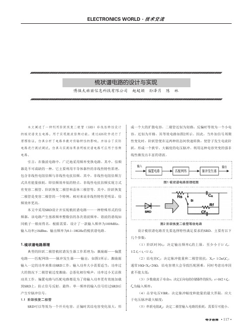
1.梳状谱电路原理典型的阶跃二极管梳状谱发生器工作原理为:激励源——偏置电路——匹配网络——脉冲发生器——输出,如图1所示。
激励源输入一定的功率来推动SRD工作,输入功率大小需要适当,功率过大的情况下二极管被过度激励,会恶化相位噪声,功率过小无法推动其工作。
偏置电路与匹配电路都是为了将输入功率更有效地加载到SRD上,防止信号反射。
最终,单一频率的输入信号经过SRD后产生窄脉冲信号。
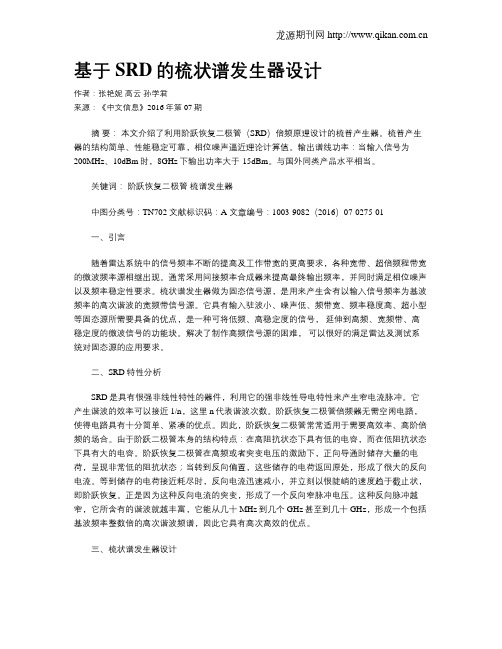
1.1 阶跃恢复二极管SRD可以等效为一个开关电容,正偏时其结电容变化很大,形成一个大的扩散电容,二极管近似为短路;反偏时等效为一个小电容,近似为开路。
其等效电路如图2所示。
因此,当外加信号周期性变化时,阶跃管便在这两种状态间快速转换,使管子发生电流阶跃,形成一个狭窄、大幅度的电压脉冲。
利用这种电容突变的强非线性激发出丰富的谐波。
图1 梳状谱电路原理框图图2 阶跃恢复二极管等效电路设计梳状谱电路首先要选择特性满足要求的SRD。
ADS veriloga 编程

Using Verilog-A in Advanced Design SystemAugust 2005NoticeThe information contained in this document is subject to change without notice. Agilent Technologies makes no warranty of any kind with regard to this material, including, but not limited to, the implied warranties of merchantability and fitness for a particular purpose. Agilent Technologies shall not be liable for errors contained herein or for incidental or consequential damages in connection with the furnishing, performance, or use of this material.WarrantyA copy of the specific warranty terms that apply to this software product is available upon request from your Agilent Technologies representative.Restricted Rights LegendUse,duplication or disclosure by the ernment is subject to restrictions as set forth in subparagraph (c) (1) (ii) of the Rights in Technical Data and Computer Software clause at DFARS252.227-7013for DoD agencies,and subparagraphs(c)(1) and (c) (2) of the Commercial Computer Software Restricted Rights clause at FAR 52.227-19 for other agencies.© Agilent Technologies, Inc. 1983-2005395 Page Mill Road, Palo Alto, CA 94304 U.S.A.AcknowledgmentsMentor Graphics is a trademark of Mentor Graphics Corporation in the U.S. and other countries.Microsoft®, Windows®, MS Windows®, Windows NT®, and MS-DOS® are U.S. registered trademarks of Microsoft Corporation.Pentium® is a U.S. registered trademark of Intel Corporation.PostScript® and Acrobat® are trademarks of Adobe Systems Incorporated.UNIX® is a registered trademark of the Open Group.Java™ is a U.S. trademark of Sun Microsystems, Inc.SystemC® is a registered trademark of Open SystemC Initiative, Inc. in the United States and other countries and is used with permission.Contents1Getting StartedUsing a Verilog-A Device in a Simulation.................................................................1-1 Modifying a Verilog-A Device....................................................................................1-5 Overriding Model Parameters on Instances.......................................................1-7 Installing Verilog-A Based Devices Provided in a Design Kit....................................1-8 Licensing..................................................................................................................1-12 2Using Verilog-A with the ADS Analog RF Simulator (ADSsim)Loading Verilog-A modules.......................................................................................2-1 The Auto Loading Mechanism............................................................................2-1 Explicit Loading of Verilog-A modules................................................................2-2 Overriding Built-in Devices.......................................................................................2-3 Using Models with Verilog-A Devices.......................................................................2-4 The Verilog-A Compiled Model Library Cache.........................................................2-5 Controlling the Auto Compilation Process................................................................2-7 Verilog-A Operator Limitations in Harmonic Balance and Circuit Envelope.............2-7 Module and Parameter Naming................................................................................2-8 Parameters...............................................................................................................2-8 Hierarchy and Module Resolution.............................................................................2-9 Modifying the Simulator’s Model Search Path..........................................................2-9 The Compiler Include Search Path...........................................................................2-9 Interaction with the Loading of Dynamically Linked UCMs.......................................2-10 3Introduction to Model Development in Verilog-ACreating a Linear Resistor in Verilog-A....................................................................3-1 Adding Noise to the Verilog-A Resistor..............................................................3-2 Creating a Linear Capacitor and Inductor in Verilog-A.............................................3-3 Creating a Nonlinear Diode in Verilog-A...................................................................3-4 Adding an Internal Node to the Diode................................................................3-5 Adding Noise to the Diode..................................................................................3-6 Adding Limiting to the Diode for Better Convergence.........................................3-6 Using Parameter Ranges to Restrict Verilog-A Parameter Values...........................3-7 Creating Sources in Verilog-A..................................................................................3-7 Creating Behavioral Models in Verilog-A..................................................................3-8 Using Hierarchy to Manage Model Complexity.........................................................3-11 4Migrating from the SDD and UCMSymbolically Defined Devices..................................................................................4-1 User-Compiled Models.............................................................................................4-8A Verilog-A in ADS Design KitsB Compilation ToolsCompiling Large Files on HP-UX..............................................................................B-1 IndexChapter 1: Getting StartedVerilog-A devices provide all of the capabilities as well as the look and feel of traditional,built-in components,with the added benefit that the end-user can choose to modify the underlying equations. A number of new devices and models are supplied with Advanced Design System to provide both new model capability as well as to provide Verilog-A versions of models that already exist as built-in models. This chapter provides an overview of the steps necessary to use Verilog-A devices. Many Verilog-A devices are provided as examples via a Design kit. For information on installing and using the Verilog-A devices supplied in the Verilog-A Design Kit, refer to“Installing Verilog-A Based Devices Provided in a Design Kit” on page1-8. Using a Verilog-A Device in a SimulationTo illustrate how Verilog-A components are used and can be modified, a popular GaAs FET model that is also supplied in the Verilog-A Design Kit (see“Installing Verilog-A Based Devices Provided in a Design Kit” on page1-8) is used in a tutorial project to show how a model can be simulated and modified. You can copy the Verilog-A Tutorial example project to your home directory or another preferred location. From the ADS Main window:1.Choose File > Copy Project.ing the Copy Project browser,click the Example Directory button and then theBrowse button to quickly locate Examples/Verilog-A/Tutorial_prj as the source.3.Specify your destination directory in the To Project field of the Copy Projectbrowser and accept the default settings to Copy Project Hierarchy and OpenProject After Copy.After the project opens, a ReadMe.dsn schematic window will appear as shown in Figure1-1 below.Getting StartedFigure1-1. The Verilog-A Tutorial_prj ReadMe.dsn4.The tutorial contains six different examples to illustrate Verilog-A components.Click the PSFETV example button on the left and then push down into thedesign.5.The example consists of a simple DC_FET curve tracer to sweep the device.Figure1-2. Simple Schematic Design using a Verilog-A Component6.Run a simulation.Note that the first time the project is simulated, the compiler will compile any un-compiled Verilog-A files found in the project’s veriloga directory.Note The compiled files, by default, reside in a cache directory in your$HOME/hpeesof directory.Getting StartedStatus / SummaryAGILENT-VACOMP (*) 2003C.day Dec 3 2003 (built: 12/04/03 01:42:48)Tiburon Design Automation (R) Verilog-A Compiler Version 0.97.120103.Copyright (C) Tiburon Design Automation, Inc. 2002-2003. All rights reserved.Compiling Verilog-A file’/users/bobl/Tutorial_prj/veriloga/psfetv.va’Loading Verilog-A module ’R’ from’/users/bobl/hpeesof/agilent-model-cache/cml/veriloga_21561_20031204_135236_007390/lib.hpux11/r esv.cml’.This module overrides the builtin ’R’ (Linear Two Terminal Resistor).HPEESOFSIM (*) 2003C.day Dec 3 2003 (built: 12/03/03 21:27:46)Copyright Agilent Technologies, 1989-2003.Loading Verilog-A module ’psfetv’ from’/users/bobl/hpeesof/agilent-model-cache/cml/veriloga_21561_20031204_135236_007390/lib.hpux11/p sfetv.cml’.CT DC_FET1.S1[1] <(GEMX netlist)> DC_FET1.VGS=(-2->0)DC DC_FET1.S1[1].DC_FET1.DC1[1/5] <(GEMX netlist)> DC_FET1.VGS=-2 DC_FET1.VDS=(0->5)..........................................DC DC_FET1.S1[1].DC_FET1.DC1[2/5] <(GEMX netlist)> DC_FET1.VGS=-1.5 DC_FET1.VDS=(0->5)..........................................DC DC_FET1.S1[1].DC_FET1.DC1[3/5] <(GEMX netlist)> DC_FET1.VGS=-1 DC_FET1.VDS=(0->5)..........................................DC DC_FET1.S1[1].DC_FET1.DC1[4/5] <(GEMX netlist)> DC_FET1.VGS=-500e-03 DC_FET1.VDS=(0->5) ..........................................DC DC_FET1.S1[1].DC_FET1.DC1[5/5] <(GEMX netlist)> DC_FET1.VGS=0 DC_FET1.VDS=(0->5)..........................................Resource usage:Total stopwatch time: 35.54 seconds.-------------------------------------------------------------------------------Simulation finished: dataset ‘tutorial_PSFETV’ written in:‘/users/bobl/Tutorial_prj/data’----------------------------------------------------------------------------If there had been a compile error, the status window would display the error and the associated line number. In this case, there were no errors and the simulation continued.Note The status window provides information about the files that werecompiled and the modules that were used. This is useful when files exist inmultiple directories.7.After the simulation is complete,open the Data Display TestBench.dds windowif necessary. The display consists of a rectangular plot with a trace of the IDS.i data. Your results should look similar to Figure1-3.Figure1-3. PSFET DCIV ResultsThe PSFETV (and any Verilog-A based device) can be used in all analyses that a traditional built-in device could be used. The PSFETV is defined in the file psfetv.va located in a directory called veriloga in the project directory. You can open and edit thefile using any text editor.You can see from thisfile that the code is relatively easy to understand. The next section will show how to modify an equation and see the effect.Other designs in the Tutorial project illustrate other key aspects of the Verilog-A language.Modifying a Verilog-A DeviceOne powerful feature of Verilog-A is that a user can make modifications to the equations that describe the behavior of the device.These changes can be available in the simulator automatically, with no loss of analysis functionality. Many models will be distributed with their source code with the expectation that end-users will modify the equations for any number of reasons. For example, the user may want the equations to better reflect some aspect of their device behavior, or they may want to delete code that is not necessary to describe their device behavior,thereby improving simulation performance.Getting StartedIn this example,the PSFETV model will be modified slightly.During simulation,the program searches for the source code based on pre-defined search paths(discussed in detail later), in the project directory veriloga, or as specifically defined using a VerilogA_Load component.1.If necessary, copy the project Tutorial_prj from the Examples/Verilog-Adirectory to a local directory. This tutorial contains a directory called veriloga that includes a file called psfetv.va. This file is a copy of the parker_skellern.va file distributed in the Verilog-A Design Kit, with the module name changed to psfetv to prevent unintended overwriting of the other model.2.Open the design file tutorial_PSFETV.dsn and run a simulation to verify thatthe results are the same as the previous example.ing any text editor, open the psfetv.va file.4.Find the equation that describes the drain current,Id:Id=Area*Beta_T*(1+lambda*Vdst)*(pow(Vgt,q)-pow(Vgt-Vdt, q));Purely for demonstration purposes, change the power law relation from “q” to “q/2” in the first power term (this has no physical meaning):Id = Area * Beta_T * (1 + lambda * Vdst) * (pow(Vgt,q/2) - pow(Vgt -Vdt, q));5.Save the file and start a simulation.Note The program will detect that the file has not been compiled and will compile the sourcefile.It will also compile other Verilog-Afiles found in the project’s veriloga directory if they have yet to be compiled, or if they are out of date.The Data Display window now shows very different results(see Figure1-4)compared to Figure1-3, demonstrating that the modification to the equation did indeed take effect.Figure1-4. PSFETV_DCIV Results using Power Law Relation of q/2Overriding Model Parameters on InstancesOne feature that most Verilog-A models implemented for ADS have is that the instance component can share all of the model parameter definitions. In most cases, the instance parameters are not visible by default, but can be edited (and made visible) from the Edit Component Parameters dialog box. Instance parameters will override the associated model parameter values. This feature provides a method to easily evaluate device mismatch,for example,since only the model parameter that is being modified needs to be changed at the instance level.Note Typically, some parameters are only available on the instance, and some parameters are only available on the model. For example, Tnom would only make sense on a model card,and Trise,the instance temperature rise over ambient,would only make sense on an instance. For this reason, the AEL definition hides these parameters from the schematic, although they are available at the netlist level.The underlying Verilog-A definition of the device is stored in a text file and, if necessary, compiled by the simulator during a simulation according to a flexible and configurable set of rules, described later.Getting StartedInstalling Verilog-A Based Devices Provided in a Design KitDesign Kits provide a convenient method for model developers to distribute new models, including those developed using Verilog-A. The use model for installing and using Verilog-A models distributed in Design Kits is the same as any other models distributed as ADS Design Kits. For more information, refer to the Design Kit Installation and Setup documentation.After properly installing the Design Kit, the components are made available on the associated palettes. The ADS release includes a Design Kit calledTIBURONDA_VERILOGA_DESIGN_KIT delivered as an unzipped file in the following location:$HPEESOF_DIR/tiburon-da/ads/designkits/tiburon-da_verilogaThis design kit includes the nonlinear models listed in Table1-1 and Table1-2. Models shown in Table1-1 are new to, or later versions of, existing models in ADS. Note All of these models are proof-of-concept models only and have not undergone the exhaustive qualification that built-ins do.Table1-1. Verilog-A Versions of Models not yet Available as Built-in Devices in ADS.Model Name DescriptionaTFT Shur-RPI amorphous silicon thin film transistor MOSFET modelBSIMSOI Version 3.1 of the BSIMSOI model familyEKV Version 2.6 of the EKV MOSFET modelHICUM_L0Level0version of the HICUM BJT model,a simplified version of thefull HICUM model.HiSIM ST ARC/Hiroshima University surface potential based MOSFETmodelParker_Skellern The Parker-Skellern MESFET model for medium powerapplications.pTFT Shur-RPI polysilicon thin film transistor MOSFET modelThe models listed in Table1-2are Verilog-A examples of models that already exist as built-in devices.Table1-2. Verilog-A Versions of Models Already Available in ADS.Model Name DescriptionAngelov Angelov GaAs FET modelBJT SPICE Gummel-Poon BJT modelBSIM3UC Berkeley BSIM3 (version 3.22)BSIM4UC Berkeley BSIM4 (version 4.3)Curtice Curtice Quadratic GaAs FET modelDiode SPICE diodeJFET SPICE silicon junction FETJunCap Philips JunCap diodeMESFET SPICE Metal Semiconductor FET modelMEXTRAM Philips Most Exquisite T ransistor model for BJT devicesMOS9Philips MOS Model 9MOS11Philips MOS Model 11TOM1T riquint’s Own Model 1TOM3T riquint’s Own Model 3VBIC Vertical Bipolar InterCompany BJT model, as released.Getting StartedUse the following procedure to install the TIBURONDA_VERILOGA_DESIGN_KIT. For more detailed information on installing and using ADS Design Kits, refer to the Design Kit Installation and Setup manual.From the ADS Main window,1.Choose DesignKit > Install Design Kits to display the Install ADS Design Kitdialog box.2.Since the Design Kit is delivered as an unzipped file, simply click the PathBrowse button under2. Define Design Kit in the Install ADS Design Kit dialog e the Select Design Kit Directory dialog box to select the following Design Kit:$HPEESOF_DIR/tiburon-da/ads/designkits/tiburon-da_veriloga3.Click OK in the Select Design Kit Directory dialog box.All associated Design Kitinformation (i.e. Path, Name, Boot File, and Version) should automaticallypopulate the appropriate fields in the Install ADS Design Kit dialog box.4.Change the Design Kit installation level from the default USER LEVEL (ifdesired) and click OK. The program will then install the Design Kit and return with a dialog box to indicate successful installation.5.Close the Install Design Kit dialog box and open a schematic window. TheDevices-Verilog-A palette should now be available in the Component PaletteList.Figure1-5 shows the icons for each of the devices and models available in the Devices-Verilog-A palette.Figure 1-5. Devices-Verilog-A Component PaletteNote To prevent unintentional overriding of the built-in versions of thesemodels, the Verilog-A modules name use an _va suffix for the name.Getting StartedLicensingThere is a single license associated with both the compilation of Verilog-A modules, and the loading of those modules into the ADSsim simulator. That license is called: sim_verilogaThere are two conditions under which the system pulls this license,•Compilation: On the compilation of the first Verilog-A file. A Verilog-A file iscompiled if the file is in the Verilog-A model path or if it is loaded via the#load command.•Loading: When a compiled Verilog-A module is loaded in the system by either #load or the auto-loading mechanisms, the system pulls a license on the first load. Note that if this Verilog-A file has just been compiled, the license hasalready been pulled. Verilog-A files that over-ride built-in devices pull a license even if they are not used.Chapter 2: Using Verilog-A with the ADS Analog RF Simulator (ADSsim)Once Verilog-A modules are loaded into the simulation environment, they may be used just like any other device in the system. A module loaded into the system takes the look and feel of a built-in ADS Analog RF Simulator (ADSsim) device. The module name becomes the device definition name, the module parameters become device parameters, and, uniquely to Verilog-A, the module may have an optional model card.Loading Verilog-A modulesADSsim has a Verilog-A model search path.Any Verilog-A module in the search path is available to be instantiated in the netlist or used on the schematic. This Verilog-A module loading mechanism is called auto loading as the search path is only traversed and modules are only loaded when the simulator encounters an unknown devicedefinition. The alternative loading mechanism is called explicit loading. In this case, the system always loads a particular Verilog-A module whether the simulator needs it or not.These loading mechanisms complement each other and are explained below in detail.During the loading process, a Verilog-A file is compiled into a shared library. These libraries are referred to as Compiled Model Libraries (CML). In general, you do not need to be concerned about the compilation process.The process has been designed to allow users to focus on writing and using Verilog-A modules rather than on the mechanics of compilation and CML file management. The system uses a CML cache. Verilog-A files are compiled once and stored for later use in the CML cache. The system manages the CML files, updating them only when necessary. As a user, you will see Verilog-A files being compiled the first time you use the files and subsequently only when you modify the files.The Auto Loading MechanismVerilog-A files (files with a.va or.vams extension) that reside in the simulator’s Verilog-A model search path are automatically compiled and loaded by the simulator, on demand, when an unknown device is encountered in the netlist. The Verilog-A model search path has four components,Using Verilog-A with the ADS Analog RF Simulator (ADSsim)PRJ_DIR/veriloga$HOME/hpeesof/veriloga$HPEESOF_DIR/custom/veriloga$HPEESOF_DIR/verilogaWhen searching for an unknown device, the system will sequentially look for a matching Verilog-A module name in each of the above directories. The first module found is loaded and a status message issued informing you that a Verilog-A module has been loaded from a particular file in the model search path.If you want the Verilog-A module to only have visibility within the current project, then create a Verilog-A directory under the current project (PRJ_DIR/veriloga) and copy the Verilog-A file to that location. Putting a Verilog-A module in the local user directory ($HOME/hpeesof/veriloga) will make it visible to simulations in all projects for this user account. The site custom directory ($HPEESOF_DIR/custom/veriloga) should be used to make Verilog-A modules available to all users of a particular ADS installation.Finally,the site directory($HPEESOF_DIR/veriloga)should not be used by you as an end user, this directory is used by Agilent Technologies to deliver new Verilog-A modules as part of the ADS system. Note that Verilog-A files placed in the site directory will not be compiled.Each file in any directory in the path must have a unique set of module names. In addition the module namespace across all files in a given directory must be unique. Having duplicate Verilog-A module names across multiple files in a directory isflagged as an error.The system cannot determine which module to use.To correct the error, modify the module names so that they are unique and re-run the simulation. Explicit Loading of Verilog-A modulesExplicit loading refers to explicitly loading all modules in a named Verilog-A file using the load component.The load component is available with the Verilog-A Design Kit.To load a file:1.Insert a VerilogA_Load component from the Devices-Verilog-A palette.e the Edit Parameters dialog box to add the name of the file to the ModuleFile Name parameter.Note that this parameter is repeatable to enable multiple files to be loaded. The component should look similar to Figure2-1.Figure2-1. The VerilogA_Load ComponentWhen the file name specified is an absolute name, the system loads the file directly. When the file name is relative, the system searches each directory in the Verilog-A model search path and loads the first file found with that name. Note that all modules in a file are loaded (unlike auto loading where only the required module is loaded into the system.)The load component netlists the#load ADS preprocessor command which has the syntax:#load "veriloga", "filename"#load is processed early in the simulation boot phase.#load commands may be placed anywhere in the netlist, but since they are preprocessor commands, there is no regard for network hierarchy.#load processing occurs before auto loading; when a device is explicitly loaded,the auto loading mechanisms are never invoked even if the device is in the search path.Overriding Built-in DevicesWhen a device has the same name as a built-in device and that Verilog-A device is in the Verilog-A model search path or is explicitly loaded,the Verilog-A device overrides the built-in device. For example, if we place a file containing a module called R in a Verilog-Afile in the model search path,then the module R will override the built-in R (the simple linear resistor).When a built-in device is overridden,the system issues a status message warning of the override as shown below.Loading Verilog-A module 'R' from'/users/bobl/hpeesof/agilent-model-cache/cml/veriloga_21561_20031204_13 5236_007390/lib.hpux11/my_resistor.cml'.This module overrides the builtin 'R' (Linear Two Terminal Resistor).Using Verilog-A with the ADS Analog RF Simulator (ADSsim)Note Overriding built-ins is a powerful and convenient way to use Verilog-A based devices in place of an existing device, but should be used with care. The system does not check that the device being loaded has the same parameter list as the built-in device that it is overriding. Without careful attention to detail, you can easily cause netlist syntax errors relating to unmatched parameters.Using Models with Verilog-A DevicesThe model card is a simulator convenience that enables you to share device parameters among multiple device instances. Each Verilog-A module loaded into the system introduces a new device and a new model - both of the same name.All parameters on a Verilog-A device may either be specified on the model, on the instance,or in both places.When a Verilog-A device references a model,itfirst reads all of the model parameters. Parameters specified directly on the instance then override the model settings. This behavior is particularly convenient when two devices share almost the same model. In this situation, they may reference a single model and override the parameters that are particular to the instances themselves. For example, let us take the diode module (PNDIODE) from the tutorial project. The module may be instantiated directly as,PNDIODE:d1 1 0 Is=3e-14 Rs=1 N=1.1 CJ0=1e-12 TT=0or it may be used more conventionally with a model card as,Model PNDIODE Dmod1 IS=3e-14 RS=1 N=1.1 CJ0=1e-12 TT=0Dmod1:d1Dmod1:d2Dmod1:d3The decision to use a model or not is your choice. Generally models are convenient when there are two or more instances that have the same parameter sets, as above where d1,d2, and d3all share the same model. We can go one step further in Verilog-A when almost all model parameters are the same. For the PNDIODE let us assume that RS i s the only parameter that varies from instance to instance. We use Dmod1 again but simply override RS on each instance that requires an RS different from the modelDmod1:d1 RS=2Dmod1:d2 RS=3Dmod1:d3 RS=4Dmod1:d4In this example,d1through d3override RS while d4inherits its value from the model, Dmod1.This model parameter inheritance with instance parameter override is ideally suited to mismatch modeling where two devices share almost the same model except for one or two parameters.While this behavior is powerful, it leads to some complications in any analysis that involves an operation that modifies a parameter.Operations that modify parameters are used in sweeping, tuning, optimization, and statistical analyses. We will use sweeping in this explanation, but the rules outlined here apply to the other analyses in exactly the same way.Device instance parameter sweeping operates in the usual way.To sweep a Verilog-A instance parameter, simply reference the parameter in the normal way in the sweep dialog box.To sweep a model parameter,reference the model parameter,again in the same way as is done for any model.When a model parameter is swept, only those instances that inherit the parameter are affected. Instances that reference the model but override the swept model parameter are not affected. When all instances override the model parameter, you will see no change in results as a function of the sweep variable. In the above example,if RS on DMod1was being swept,then the only instance affected by the sweep would be d4.Note Only those model parameters that are actually specified on the model card may be swept. This is a model only limitation.The Verilog-A Compiled Model Library CacheWhen Verilog-A modules are compiled,they are stored in a directory cache,which by default is created at,$HOME/hpeesof/agilent-model-cache/This cache is created the first time a Verilog-A file is compiled and entries are added or updated as Verilog-A files are compiled. An existing cache may be moved to a new location, but cache contents may not be modified in any way.。
基于SRD的梳状谱发生器设计

基于SRD的梳状谱发生器设计本文介绍了利用阶跃恢复二极管(SRD)倍频原理设计的梳普产生器。
梳普产生器的结构简单、性能稳定可靠,相位噪声逼近理论计算值。
输出谱线功率:当输入信号为200MHz、10dBm时,8GHz下输出功率大于-15dBm。
与国外同类产品水平相当。
标签:阶跃恢复二极管梳谱发生器一、引言随着雷达系统中的信号频率不断的提高及工作带宽的更高要求,各种宽带、超倍频程带宽的微波频率源相继出现。
通常采用间接频率合成器来提高最终输出频率,并同时满足相位噪声以及频率稳定性要求。
梳状谱发生器做为固态信号源,是用来产生含有以输入信号频率为基波频率的高次谐波的宽频带信号源。
它具有输入驻波小、噪声低、频带宽、频率稳度高、超小型等固态源所需要具备的优点,是一种可将低频、高稳定度的信号,延伸到高频、宽频带、高稳定度的微波信号的功能块。
解决了制作高频信号源的困难,可以很好的满足雷达及测试系统对固态源的应用要求。
二、SRD特性分析SRD是具有很强非线性特性的器件,利用它的强非线性导电特性来产生窄电流脉冲。
它产生谐波的效率可以接近1/n,这里n代表谐波次数。
阶跃恢复二极管倍频器无需空闲电路,使得电路具有十分简单、紧凑的优点。
因此,阶跃恢复二极管常常适用于需要高效率、高阶倍频的场合。
由于阶跃二极管本身的结构特点:在高阻抗状态下具有低的电容,而在低阻抗状态下具有大的电容。
阶跃恢复二极管在高频或者突变电压的激励下,正向导通时储存大量的电荷,呈现非常低的阻抗状态;当转到反向偏置,这些储存的电荷返回原处,形成了很大的反向电流。
等到储存的电荷接近耗尽时,反向电流迅速减小,并立刻以很陡峭的速度趋于截止状,即阶跃恢复。
正是因为这种反向电流的突变,形成了一个反向窄脉冲电压。
这种反向脉冲越窄,它所含有的谐波就越丰富,它能从几十MHz到几个GHz甚至到几十GHz,形成一个包括基波频率整数倍的高次谐波频谱,因此它具有高次高效的优点。
三、梳状谱发生器设计梳状谱发生器电路框图如图1所示,为了获得丰富的谐波输出,就要使阶跃恢复二极管能产生较大的窄电流脉冲,需要先将输入信号放大到一定的功率来推动阶跃恢复二极管。
阶跃恢复二极管倍频器的设计

阶跃恢复二极管倍频器的设计
阶跃恢复二极管倍频器的设计
阶跃恢复二极管倍频器是一种常见的电路,它可以将输入信号的频率倍增。
在设计阶跃恢复二极管倍频器时,需要考虑以下几个方面。
1. 选择合适的二极管
阶跃恢复二极管倍频器中使用的二极管需要具有快速的恢复时间和低的串扰。
常用的二极管有PIN二极管和Schottky二极管。
PIN二极管具有较快的恢复时间和较低的串扰,但其反向电容较大;Schottky二极管的反向电容较小,但其恢复时间和串扰较大。
因此,在选择二极管时需要根据具体的应用场景进行权衡。
2. 选择合适的电容和电感
阶跃恢复二极管倍频器中使用的电容和电感需要具有较高的品质因数和较低的损耗。
常用的电容有瓷片电容和铝电解电容;常用的电感有空心电感和铁氧体电感。
在选择电容和电感时,需要根据具体的应用场景进行权衡。
3. 设计合适的匹配网络
阶跃恢复二极管倍频器中使用的匹配网络需要将输入信号和输出信号的阻抗匹配。
常用的匹配网络有L型匹配网络和T型匹配网络。
在设计匹配网络时,需要根据具体的应用场景进行权衡。
4. 优化电路布局
阶跃恢复二极管倍频器中的电路布局需要尽可能减少信号的串扰和反射。
常用的优化方法有增加地面平面、减少信号线长度、增加信号线间距等。
在优化电路布局时,需要根据具体的应用场景进行权衡。
总之,阶跃恢复二极管倍频器的设计需要考虑多个方面,包括选择合适的二极管、电容和电感、设计合适的匹配网络以及优化电路布局。
只有在综合考虑这些因素的基础上,才能设计出性能优良的阶跃恢复二极管倍频器。
基于SRD的梳状谱发生器设计
基于SRD的梳状谱发生器设计作者:张艳妮高云孙学君来源:《中文信息》2016年第07期摘要:本文介绍了利用阶跃恢复二极管(SRD)倍频原理设计的梳普产生器。
梳普产生器的结构简单、性能稳定可靠,相位噪声逼近理论计算值。
输出谱线功率:当输入信号为200MHz、10dBm时,8GHz下输出功率大于-15dBm。
与国外同类产品水平相当。
关键词:阶跃恢复二极管梳谱发生器中图分类号:TN702 文献标识码:A 文章编号:1003-9082(2016)07-0275-01一、引言随着雷达系统中的信号频率不断的提高及工作带宽的更高要求,各种宽带、超倍频程带宽的微波频率源相继出现。
通常采用间接频率合成器来提高最终输出频率,并同时满足相位噪声以及频率稳定性要求。
梳状谱发生器做为固态信号源,是用来产生含有以输入信号频率为基波频率的高次谐波的宽频带信号源。
它具有输入驻波小、噪声低、频带宽、频率稳度高、超小型等固态源所需要具备的优点,是一种可将低频、高稳定度的信号,延伸到高频、宽频带、高稳定度的微波信号的功能块。
解决了制作高频信号源的困难,可以很好的满足雷达及测试系统对固态源的应用要求。
二、SRD特性分析SRD是具有很强非线性特性的器件,利用它的强非线性导电特性来产生窄电流脉冲。
它产生谐波的效率可以接近1/n,这里n代表谐波次数。
阶跃恢复二极管倍频器无需空闲电路,使得电路具有十分简单、紧凑的优点。
因此,阶跃恢复二极管常常适用于需要高效率、高阶倍频的场合。
由于阶跃二极管本身的结构特点:在高阻抗状态下具有低的电容,而在低阻抗状态下具有大的电容。
阶跃恢复二极管在高频或者突变电压的激励下,正向导通时储存大量的电荷,呈现非常低的阻抗状态;当转到反向偏置,这些储存的电荷返回原处,形成了很大的反向电流。
等到储存的电荷接近耗尽时,反向电流迅速减小,并立刻以很陡峭的速度趋于截止状,即阶跃恢复。
正是因为这种反向电流的突变,形成了一个反向窄脉冲电压。
基于Verilog-A的流水线型ADC数字校正技术仿真平台

1引言随着信息技术的进一步发展,微电子芯片集成度不断提高,芯片尺寸越来越小。
工艺尺寸的缩小意味着特征线宽不断降低。
在这一背景下:一方面,器件速度进一步提高,功耗进一步降低;另一方面,晶体管本征增益降低,工作电源电压降低。
此时,数字电路的速度更快,功耗更低,所以数字电路会持续受益;而对于模拟电路来说,电源电压、本征增益的降低意味着高增益的放大器设计越来越困难。
所以,工艺的演进对于模拟电路来说是一种挑战。
在很多的应用场合,模拟电路趋向于用更多的数字电路来代替。
模数转换器(ADC )作为将模拟信号转换为数字信号的装置,起着连接模拟世界与数字世界桥基于Verilog-A 的流水线型ADC数字校正技术仿真平台宫月红1,张少君1,罗敏2,王明雨1,刘冰冰1(1.山东交通学院船舶与轮机工程学院,威海264209;2.哈尔滨工业大学(威海)微电子中心,威海264209)摘要:为了对流水线型ADC 数字校正技术进行研究,提出了一种基于Verilog-A 的行为级仿真平台。
在该平台中,采用Verilog-A 语言对流水线型ADC 中各个组成模块进行建模、采用Volterra 级数对系统误差进行模拟、采用Verilog 语言对数字校正算法进行建模。
应用此平台,结合一种确定性的数字校正技术对一个12位分辨率,1.5位每级结构,40MHz 采样速度的流水线型ADC 进行了仿真。
在芯片设计之前使用该平台进行仿真,不仅能够有效地缩短流水线型ADC 数字校正技术的硬件设计周期,还提高了校正算法开发的灵活性和实用性,从而对进一步提高流水线型ADC 的性能、降低功耗起到重要的促进作用,具有很高的实用价值。
关键词:Verilog-A 语言;仿真平台;流水线型ADC ;数字校正;Volterra 级数DOI :10.3969/j.issn.1002-2279.2018.02.011中图分类号:TP312文献标识码:A 文章编号:1002-2279(2018)02-0042-05Pipeline ADC Digital Correction Technology Simulation PlatformBased on Verilog-AGONG Yuehong 1,ZHANG Shaojun 1,LUO Min 2,WANG Mingyu 1,LIU Bingbing 1(1.Naval Architecture &Marine Engineering College,Shandong Jiaotong University,Weihai 264209,China ;2.Harbin Institute of Technology Weihai Microelectronics Center,Weihai 264209,China )Abstract:To research pipeline ADC digital calibration technique,a Verilog -A based behavioral simulation platform is proposed.In this platform,Verilog-A language is adopted to mimic the modules in pipeline ADC,Volterra series theory is applied to imitate system error,Verilog language is employed to module digital algorithm.Applying this platform,a 10bits,1.5per stage structure,50MHz sample speed background calibration pipeline ADC with a deterministic calibration algorithm is simulated.Applying this platform in simulation before chip design can not only reduce pipeline ADC digital calibration technique design cycle,but also improve calibration algorithm developing flexibility and practicability.Thus,pipeline ADC performance can be further improved,and power consumption can be further reduced,so it has high practical value.Key words:Verilog-A;Simulation platform;Pipeline ADC;Digital calibration;Volterra作者简介:宫月红(1982—),女,河北省衡水市人,博士,讲师,主研方向:模拟混合信号集成电路设计与数字信号处理。
用阶跃恢复二极管设计16次倍频器 2J5J

2 16 次倍频器的实现
2.1 管子的选择 阶跃管的主要参数为 反偏电容 Cj 少数载流子
寿命τ 转换时间 tt 串联正向传导电阻 Rs 击穿电压
VB 在倍频器设计中对这些参数的要求如下
1
10Ω <
1 2πf N C j
< 20Ω
2
τ
>>
1 2π
f1
3
tt
≤
1 fN
Rs 应尽量小 VB 应大于脉冲幅度 根据以上要求
偏置网络为二极管提供一个合适的偏压 使得
SRD 恰好在负电流最大的瞬间产生电流阶跃 以便得
到尽可能大的电流阶跃值 图 2 中所示为自给偏压
是由二极管的直流分量通过偏压电阻 Rb 时产生电压 降而得 Lb 为高频扼流圈 用以防止 Rb 对高频分流 Cb 为隔直电容 可以防止或削弱偏置电路与信号源之 间不必要的耦合[2,3]
出功率 7 dBm 放大器采用 Mini 公司的 Gali 4 对 于 100 MHz 信号增益可达 11 dB 放大后产生足够驱 动脉冲发生器工作的激励信号 由于输出频率不算高
若采用微带滤波器会增大整个倍频器的体积 因此采
用集总参数的带通滤波器 中心频率 1.6 GHz 带内 衰减 5 dB 1.5 GHz 和 1.7 GHz 处抑制均达 60 dB 由 于滤波器带内衰减较大 后面还需加一级放大才能达
5 的高次倍频 当倍频效率较低时 可通过加放大
器来弥补 当倍频次数高达几十次时 为实现较高的
倍频效率 可以用两级或多级倍频 当然 级数越多
调试起来越困难 整个系统的体积也会增大 因此实
际设计中需要权衡
参考文献
[1] 薛正辉, 杨仕明, 李伟明, 等. 微波固态电路 [M]. 北京: 北京理工大 学出版社, 2004. 198–206.
阶跃恢复二极管测量
阶跃恢复二极管测量
阶跃恢复二极管测量是一种用于测量二极管参数的方法。
在这种方法中,一个阶跃电压被施加到二极管的正向偏置,然后测量其反向恢复时间。
实施阶跃恢复测量的步骤如下:
1. 将二极管连接到一个恒流源,以确保二极管的正向电流是恒定的。
2. 在二极管的正向偏置电路上施加一个阶跃电压信号。
3. 使用一个示波器来测量二极管的正向电压响应。
4. 停止施加阶跃电压,并测量二极管的反向电流恢复时间。
根据测量结果,可以计算出二极管的一些参数,如恢复时间、反向电流峰值等。
这些参数反映了二极管的动态特性和性能。
阶跃恢复二极管测量是一种比较简单和直观的方法,常用于测量二极管的开关速度和功耗等性能指标。
它可以帮助工程师评估二极管在特定应用中的可靠性和性能是否符合要求。
- 1、下载文档前请自行甄别文档内容的完整性,平台不提供额外的编辑、内容补充、找答案等附加服务。
- 2、"仅部分预览"的文档,不可在线预览部分如存在完整性等问题,可反馈申请退款(可完整预览的文档不适用该条件!)。
- 3、如文档侵犯您的权益,请联系客服反馈,我们会尽快为您处理(人工客服工作时间:9:00-18:30)。
This document is owned by Agilent Technologies, but is no longer kept current and may contain obsolete or inaccurate references. We regret any inconvenience this may cause. For the latest information on Agilent’s line of EEsof electronic design automation (EDA) products and services, please go to:/fi nd/eesofAgilent EEsof EDANonlinear Modeling of Step RecoveryDiodes using Verilog-AEagleware App Note 22 Nonlinear Modeling of Step Recovery Diodes UsingVerilog-AIntroductionThe Advanced Modeling Kit (AMK) in GENESYS contains an innovative Verilog-A compiler. This nonlinear modeling tool enables both the semiconductor modeling industry and design engineers to create and implement new complex linear and non-linear models that cover a wide range of behavioral characteristics. Verilog-A CompilerBased on the IEEE Verilog-A standard, extensive libraries of functions and an intuitive language help modelers and design engineers develop and deploy new functionality in minimum time. Illustrating the flexibility and utility available with the AMK, GENESYS offers VBIC, HiSIM, MEXTRAM and other models in Verilog-A source code and compiled models. Verilog-A source code is easier to read, requires less lines of code, and - after compilation - runs nearly as fast as a model written in C-code. The AMK does not limit the designer to pre-established models, although new models or features can be developed by using an existing model as a foundation. With the AMK you can develop models to describe and simulate the behavior of transistors, FETs, diodes, laser diodes, PIN receivers, non-linear magnetic devices and more.The design procedure starts with a text editor. Either from scratch or from one of the many Verilog-A examples, a text file is developed that describes the terminal behavior of the device. In many cases the temperature and parasitic dependencies are also modeled and a table of parameters is established, enabling users of the model to enter additional parametric characteristics. Once the text file is complete, the file is stored in the “My Models” directory with a va name extension. When GENESYS is started, any va files are automatically compiled and linked into the GENESYS engine. The new model can then be used in the same manner as any other model in the design environment. Modeling a Step Recovery Diode A model of a step recovery diode was implemented to illustrate the use of the AMK. The step recovery diode (SRD), or “snap diode,” has an unusual operating characteristic whenever forward biased charge is stored in the depletion region. During the reverse cycle, when the stored charge is removed, the conduction abruptly halts. This abrupt halt explains the diode’s name: “snap diode”. The abrupt current change is utilized to produce sampling devices and frequency multipliers.To develop the SRD model we start with the Verilog-A description of a SPICE-like non-linear diode. From this starting point we add parameters describing the diode’s capacitance, lead inductance, reverse recovery time, series resistance and other diode parameters. Next, the section that describes the capacitance/charge characteristics is modified to mimic the charge characteristics vs. voltage of a step recovery diode (See Appendix). When completed, the file is saved in the ‘My Models’ directory and when GENESYS is next started it automatically checks for new file revisions, compiles and loads the model for use. The only additional feature to add is a custom symbol, if desired. The process completed, the SRD model is now available for simulation via the parts library manager or pull-down menus.May 2004 Eagleware Corporation 1VmComb GeneratorFigure 1 shows the design of a comb generator using the AMK-created model. Simulation was completed with GENESYS HARBEC using 30 harmonics with an input frequency of 200 MHz and power of +26 dBm.Figure 1The topology in Figure 1 uses the typical series inductance L1 to provide the impulse shape. As stated previously, when the diode currentabruptly shuts off as a result of the forward bias charge being depleted, a voltage spike isgenerated as a result of L di/dt. The pulse width is usually designed either to produce a rich set of harmonics—such as in the comb generator example for broadband mixing, Figure 1, or shaped to enhance a particular multiple of the input frequency as illustrated in the X10multiplier in Figure 5. The additional lumped components, L2 and C3, provide a match to the source impedance at the driven frequency 1.Figure 2Figure 2 notes the voltage waveforms at the input of the comb generator and at the junction 1Hewlett Packard Application Note 920of L1, L2, and C1. Note that the impulse has not been totally filtered at this point. Figure 3 shows the impulse generated into the 50 ohm load.By varying parameters such as junctioncapacitance, reverse recovery time, and parasitic inductance, different pulse shapes optimized for the task required can be manipulated based upon manufacturer’s data sheets. Figure 4 illustrates a non-optimized comb. Note that power drops by only 10db up to the 15th harmonic.Figure 4Vm10X Multiplier ExampleTo further illustrate the potential gain in using the AMK, a 10X multiplier was simulated.Starting with the basic comb generator design, a frequency selective output resonator, consisting of a length of transmission line and coupling capacitor, was added. Figure 5 illustrates the final schematic configuration.Figure 5Once a final design is realized, the Advanced T/LINE feature in GENESYS converts thetransmission topologies into their final form (i.e. microstrip) without further effort by the designer. The node voltages for the completed multiplier are shown in Figures 6 and 7.Figure 6Figure 6 shows the input waveform and that of the impulse at the diode/transmission line node.Figure 7 illustrates the ringing waveform at the 50 load. The electrical length, line impedance, and coupling capacitor all affect the shape and frequency response of the final signal. The goal of varying these component values is to maximize the power available in Nth comb.2 Finally, Figure 8 provides a look at the output spectrum centered around 2 GHz (X10 of input frequency). Typically, additional filtering is required if the multiplier has more stringent harmonic content requirements. This may be implemented with lumped or distributed filters that are dictated by the operating frequency.Fortunately GENESYS offers synthesis tools that cover the range with M/FILTER and FILTER. Figure 82Hewlett Packard Application Note 918Appendix/*Eagleware 2003 Bill ClausenImplementation of a step recovery diode as defined by Zhang and Raissanen in"A New Model of Step Recovery Diode for CAD" MTT-S 1995 p 1459-1462*/`include "constants.vams"`include "disciplines.vams"`define SPICE_GMIN 1.0e-12`define LARGE_REAL 1.0e99`define DEFAULT_TNOM 27module diode_srd(anode,cathode);// %%DEVICE_CLASS=DIODE%%inout anode, cathode;electrical anode, cathode, internal;parameter real Area = 1.0 from (0:inf]; //Area scaling factorparameter real Is = 1e-14 from [0:inf]; //Saturation current [A]parameter real Tnom = `DEFAULT_TNOM from (-`P_CELSIUS0:inf); //Measurement temp[C]parameter real Rs = 0.0 from [0:inf]; //Ohmic res [Ohm]parameter real Rf = 0.1 from [0:inf]; // Forward biased resistance[Ohm]parameter real Tt = 0.0 from [0:inf]; //Transit time [s]parameter real Tau = 2e-9 from [0:inf]; // Reverse recovery time[s]parameter real Cr = 0.0 from [0:inf]; //Junction capacitance [F]parameter real Lpk = 1e-9 from [0:inf]; //Package Inductance [H]parameter real Cpk = 2e-12 from [0:inf]; // Package Capacitance[F]parameter real Vj = 1.0 exclude 0; //Junction potential [V]parameter real N = 1.0 from [0:inf]; //Emission coefparameter real M = 0.5 from [0:inf]; //Grading coefparameter real Eg = 1.11 from (0:inf]; //Activation energy [eV]parameter real Xti = 3.0 from [0:inf]; //IS temp exp.parameter real Kf = 0.0; //Flicker noise coefparameter real Af = 1.0 from (0:inf); //Flicker noise exponentparameter real Fc = 0.5 from [0:1]; //Forward bias junct parmparameter real Bv = 60.0 from [0:inf]; //Reverse breakdown voltage [v]parameter real Ibv = 0.001 from [0:inf];//Current at BV [A]real Vd, Id, Qd, Cf;real f1, f2, f3, Fcp;real Ibv_calc, Vth;real Is_temp, Vth_nom, T_nom, T;analog beginVth = $vt;T = $temperature;f1 = (Vj/(1 - M))*(1 - pow((1 - Fc), 1 - M));f2 = pow((1 - Fc), (1 + M));f3 = 1 - Fc * (1 + M);Fcp = Fc * Vj;Cf = Tau/Rf;if (Ibv !=0)Ibv_calc = Ibv;elseIbv_calc = Is * Bv / Vth;Vd = V(anode, internal);// Temperature dependenceT_nom = Tnom + `P_CELSIUS0;Vth_nom = $vt(T_nom);Is_temp = Is * pow(T/T_nom, Xti / N) * limexp(Eg / Vth_nom - Eg / Vth);May 2004 Eagleware Corporation 4AN-22 Nonlinear Modeling of Step Recovery Diodes Using Verilog-A// Intrinsic diode// BV is not adjusted to match Ibv if I(BV) <> Ibvif (Vd < 0) beginif (Vd < -Bv) // Past breakdownId = -Area * Is_temp * (limexp(-(Bv + Vd) / Vth) + Bv / Vth);else if (Vd == -Bv) // At breakdownId = -Area * Ibv_calc;else if (Vd <= -5 * N * Vth) // -Bv < Vd < -5 nKT/qId = -Area * Is_temp + Vd * `SPICE_GMIN;else // -5 nKT/q <= Vd < 0Id = Area * Is_temp * (limexp(Vd / Vth) - 1) + Vd * `SPICE_GMIN;endelse // Fwd bias:Id = Area * Is_temp * (limexp(Vd / (N * Vth)) - 1) + Vd * `SPICE_GMIN;// Capacitance (junction and diffusion)if (Vd <= 0)Qd = Cr*Vd;else if ((Vd > 0.0)&&(Vd < Fcp))Qd = (Cf-Cr/2*Fcp)*pow((Vd+(Cr*Fcp)/(Cf-Cr)),2)-(Cr*Cr*Fcp)/(2*(Cf-Cr));elseQd = Cf*Vd-(Cf-Cr)*Fcp/2;I(anode, internal) <+ Id;V(internal, cathode) <+ I(internal, cathode) * (Rs / Area) + Lpk*ddt(Id);I(anode, internal) <+ ddt(Qd);endendmoduleReferencesAdditional Sources of Information1)“A Circuit Model of the Step Recovery Diode,” K.L. Kotzebue, Proceedings of the IEEE,December, 1965, pg 2119-2120.2)“Computer Aided Design of Step Recovery Diode Frequency Multipliers,” Jian Zhang and AnttiV. Raisanen, MTT, vol 44, No.12, December, 1996, pg 2612-2616.3)“Shunt Harmonic Generation Using Step Recovery Diodes,” Stephen Hamilton, Robert Hall,Microwave Journal, April 1967, pg 69-78.4)“Pulse and Waveform Generation with Step Recovery Diodes,” Hewlett Packard Application Note918.5)“Harmonic Generation Using Step Recovery Diodes and SRD Modules,” Hewlett PackardApplication Note 920.6)“Ku-band Step Recovery Multipliers,” Hewlett Packard Application Note 928.7)“Comb Generator Simplifies Multiplier Design,” Hewlett Packard Application Note 983./fi nd/emailupdatesGet the latest information on the products and applications you select./fi nd/agilentdirectQuickly choose and use your testequipment solutions with confi dence.Agilent Email UpdatesAgilent DirectFor more information on Agilent T echnologies’products, applications or services, please contact your local Agilent office. The complete list is available at:/fi nd/contactusAmericasCanada (877) 894-4414 Latin America 305 269 7500United States (800) 829-4444Asia Pacifi c Australia 1 800 629 485China 800 810 0189Hong Kong 800 938 693India 1 800 112 929Japan 0120 (421) 345Korea 080 769 0800Malaysia 1 800 888 848Singapore 1 800 375 8100Taiwan 0800 047 866Thailand 1 800 226 008 Europe & Middle East Austria 0820 87 44 11Belgium 32 (0) 2 404 93 40 Denmark 45 70 13 15 15Finland 358 (0) 10 855 2100France 0825 010 700* *0.125 €/minute Germany 01805 24 6333****0.14 €/minuteIreland 1890 924 204Israel 972-3-9288-504/544Italy 39 02 92 60 8484Netherlands 31 (0) 20 547 2111Spain 34 (91) 631 3300Sweden 0200-88 22 55Switzerland 0800 80 53 53United Kingdom 44 (0) 118 9276201Other European Countries: /fi nd/contactusRevised: March 27, 2008Product specifi cations and descriptions in this document subject to change without notice.© Agilent Technologies, Inc. 2008For more information about Agilent EEsof EDA, visit:/fi nd/eesofPrinted in USA, May 01, 2004 5989-8899EN。