
Type C协会标准规范
All dimensions for component level qualification and overmold only for cable and adaptor assembles No EMC shielding
spring finger tip of the USB full featured type C plug or USB 2.0 type C plug shall be exposed in the plug housing opening of the unmated type C plug
NA
Type C pin A5 resistance to GND for cableassemblies with a USB
B plug Type C pin A5 to Vbus resistance for cableassemblies with a standard A plug
EIA-364-90 NA NA NA NA NA
Single-ended coupling between SBU_A and SBU_B
Single-ended coupling between SBU_A/SBU_B and differential USB D+/D-
Vbus loop inductance
The limit is defined with the vertices of (0.3MHz, -56.5dB), (1MHz, -46dB), (10MHz, -26dB), (11.2MHz, 25dB) and (100MHz, -
log11(f) For USB full featured type C, the singled-
ended couppling between CC and Dshall be below the limits defined with the vertices of (0.3MHz, -58dB), (10MHz, -27.5dB), (11.8MHz, -26dB), and
D+/D- pair differential impedance
D+/D- 衰減差 D+/D- pair Propagation
Delay D+/D- pair 傳播延遲
75 ohms to 105 ohms 20 ns max
D+
SBU_B and CC
Single-ended coupling between CC and D-
The limit is defined with the vertices of
(0.3MHz, -65dB), (1MHz, -55dB), (18MHz, -30dB), and (100MHz, -
Group B-2 USB2.0 and low speed signal tests of Type C cable and adaptor assemblies
Type C-C
D+/D- pair attenuation D+/D- 衰減
≧-1.02dB@50MHz ≧-1.43dB@100MHz ≧-2.40dB@200MHz ≧-4.35dB@400MHz
在循環操作時不會斷開
4-axis continuity 四軸向
No discontinuity greater than 1 us duration in any of the four orientation
tested 在四個方向測試無大於
1us的瞬斷
Voltage Drop 壓降
250mV for GND and 500mV for Vbus
dB
Integrated crosstalk on superspeed pairs (INEXT
and ISXT)
Integrated near-end crosstalk:
INEXT≦-40 dB to 12.5 GHz, for TX1 to RX1, TX2 to RX2, Tx2 to RX1, TX1 to RX2, TX1 to TX2 and RX1 to RX2
≧-6 dB at 5 GHz ≧-11 dB at 10 GHz
For all USB 3.1 Gen1 super speed pairs: ≧-7 dB at 2.5 GHz ≧-12 dB at 5 GHz
≦0.126 ILfitatNq^2+3.024. ILfitatNq-23.392, in
25dB) in scale of log10(f)
The limit is defined with the vertices of
(0.3MHz, -80dB), (30MHz, -40dB) and (100MHz, -40dB) in scale of log10(f)
≦ 900 nH
Vbus capacitance
8 nF to 500 nF in each Type C plug
Inductance coupling factor between Vbus and Other low
speed signal
<= 0.3
Rd resistor verification
NA
Rp resistor verification
NA
EIA-364-90
NA
EIA-364-90
NA
EIA-364-90
NA
EIA-364-90
NA
NA Do not support PD: 8 nF to 12 nF located in the Type C plug
Support PD: 80 pF to 120 pF located in the Type C plug
Differential model: ≦-55 dB for f≦1.6
GHz ≦-50 dB for 1.6 GHz ≦f ≦ 4.0 GHz and for
5 GHz ≦f ≦6 GHz
Group B-5 Critical Dimension
Type C-C
Critical Dimension
Integrated crosstalk between superspeed pairs
and D+/D(IDDEXT_1NEXT+FEXT and,
IDDXT_2NEXT)
Integrated near-end crosstalk to D+/D-: IDDXT_2NEXT≦-33 dB Integrated near-end and far-end crosstalk
that causes discontinuity or
shorting No discontinuity or
shorts allowed
No disruptive dicharge
The plug shall disengage from the
test fixture or mechanically fail, when a moment of 2.0 Nm is applied in the up and down direction, and a moment 3.5 Nm is applied in the left and right direction
測試方法
EIA-364-38b 軸向掛重至少1分鐘
EIA-364-41 X=3.7 x cable 直徑, 100次循環,
2平面, 120度角度
pys標準
Use the highest rated current for the cable assembly
Type C-Legacy ≧-1.02dB@50MHz ≧-1.43dB@100MHz ≧-2.40dB@200MHz ≧-4.35dB@400MHz
NA
≦0.046 ILfitatNq^2+1.812. ILfitatNq-10.784, in
dB
≦ -20dBfrom 100 MHz to 10 GHz
Group B-4 USB Type C cable assembly shielding effectiveness
Type C-C
Cable shielding effectiveness
Group B-1 Type C connector and cable assembly mechanical tests
Cable pull out 線材吊重
協會標準 40 N Minmum, 線材組裝 需無電性斷開且線材不會
從CONN分離
Cable flex 線材柔軟
No loss of continuity during cycling
to D+/D-: IDDXT_1NEXT+FEXT≦-
34.5 dB For all superspeed
pairs
Integrated Differential crosstalk on D+/D- (IDDXT)
Integrated return loss (IRL)
Differential to common mode conversion (SCD12/SCD21)
26dB) in scale of log10(f)
For USB 2.0 Type C cables, the singled-
ended couppling between CC and Dshall be below the limits defined with the vertices of (0.3MHz, -48.5dB), (1MHz, -38dB), (10MHz, -18dB), and (100MHz, 18dB) in scale of
TYPEC数据线规格书

T Y P E C数据线规格书V1.0关键词:TYPE C、数据线摘要:本文介绍了数据线的规格,性能及测试规范。
缩略语:1范围标准适用于TYPE A TO C数据线需求规格书,未尽规格描述以TYPE C协会规范V1.1为准。
2编写依据3数据线正常工作和存储条件3.1数据线应能在下列条件下正常工作:3.1.1 工作环境温度:-20℃~+55℃;(仅作单体验证目的,与整机匹配时以整机试验环境为准);3.1.2 相对湿度:5%~95%;3.1.3 大气压力:86 kPa~106kPa;3.1.4 数据线的存储温度:-40℃~+85℃;4数据线主要参数4.1数据线连线规格详细尺寸以及工艺要求以3D图档为准1、type C金属插头,要求必须是整体拉伸成型,不能是折弯成型,不接受接缝;2、金属插头部分,要求做不锈钢原色,表面喷砂处理: 50u”~150u”MA TT NICKEL PLATING OVER ALL3、保证至少3A通流能力整条线缆产品详细规格(BOM清单, 包括端子图纸2D & 可拆解版本的3D)要有确认才能认可(认证时必须提供以上文件)。
4.2线材主体信息:4.2.1外观5V/3A A plug TO C plug, cover式,白色半雾面,素材细咬花处理,MT110064.2.2主体结构导体材质规格如下:材质:镀锡铜绝缘材质NON-PVC,须满足5.2章节测试性能要求4.2.3关键尺寸4.2.3.1USB2.0 B plug参考协会规范4.2.3.2TYPE C plug1.红圈标示尺寸为重点尺寸,其余尺寸依据协会规范要求2.各组件BOM LIST原材料信息需明确到具体牌号3.应满足TYPE C 2.0规格4.2.3.3镀层厚度测试区域规定关于镀层测试区域和方法:TYPE C/A:TYPE C/A 产生接触的关键区域为PIN针头部触点,因此镀层工艺为考虑成本一般只覆盖PIN针触点位置,其他区域为flash Au,所以镀层的量测范围定义在PIN针触点弧顶的最高处4.2.4线序镀层厚度为在触点弧顶最高点0.5mm 的范围内进行测量,同一触点在0.5mm 范围内测量三次取平均值0.5mm5技术要求5.1线材外观要求5.1.1线材外观要求如下:未尽事宜参考《终端数据线检验通用操作指导书》5.2线材性能要求Test conditionTemperature:15℃to 35℃Air pressure :86 to106 kPa Relative humidity:25% to 85%5.3安全性要求USB数据线的安全性能应能满足CCEE规定要求。
(仅供参考)USB Type-C 3.1协会规范
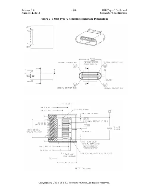
Figure 3-1 USB Type-C Receptacle Interface DimensionsFigure 3-1 USB Type-C Receptacle Interface Dimensions, cont.Figure 3-2 Reference Design USB Type-C Plug External EMC Spring Contact ZonesFigure 3-3 USB Full-Featured Type-C Plug Interface DimensionsFigure 3-4 Reference Footprint for a USB Type-C Vertical Mount Receptacle(Informative)Figure 3-5 Reference Footprint for a USB Type-C Dual-Row SMT Right AngleReceptacle (Informative)Figure 3-6 Reference Footprint for a USB Type-C Hybrid Right-Angle Receptacle(Informative)Figure 3-7 Reference Footprint for a USB Type-C Mid-Mount Dual-Row SMT Receptacle(Informative)Figure 3-8 Reference Footprint for a USB Type-C Mid-Mount Hybrid Receptacle(Informative)This specification requires that all contacts be present in the mating interface of the USB Type-C receptacle connector, but allows the plug to include only the contacts required for USB PD and USB 2.0 functionality for applications that only support USB 2.0. The USB 2.0 Type-C plug is shown in Figure 3-9. The following design simplifications may be made when only USB 2.0 is supported:∙Only the contacts necessary to support USB PD and USB 2.0 are required in the plug.All other pin locations may be unpopulated. See Table 3-5. All contacts are required to be present in the mating interface of the USB Type-C receptacle connector.∙Unlike the USB Full-Featured Type-C plug, the internal EMC springs may be formed from the same strip as the signal, power, and ground contacts. The internal EMC springs contact the inner surface of the plug shell and mate with the receptacle EMC pads when the plug is seated in the receptacle.∙ A paddle card inside the plug may not be necessary if wires are directly attac hed to the contact pins.Figure 3-9 USB 2.0 Type-C Plug Interface Dimensions3.2.2Reference DesignsThis section provides reference designs for a few key features of the USB Type-C connector. The reference designs are provided as acceptable design examples. They are not normative.3.2.2.1Receptacle Mid-Plate (Informative)The signals between the top and bottom of the receptacle tongue are isolated by a mid-plate inside the tongue. Figure 3-10 shows a reference design of the mid-plate. It is important to pay attention to the following features of the middle plate:∙The distance between the signal contacts and the mid-plate should be accurately controlled since the variation of this distance may significantly impact impedance of the connector.∙The mid-plate in this particular design protrudes slightly beyond the front surface of the tongue. This is to protect the tongue front surface from damage caused by miss-insertion of small objects into the receptacle.∙The mid-plate is required to be directly connected to the PCB ground with at least two grounding points.∙The sides of the mid-plate mate with the plug side latches, making ground connections to reduce EMC. Proper surface finishes are necessary in the areaswhere the side latches and mid-plate connections occur.Figure 3-10 Reference Design of Receptacle Mid-Plate3.2.2.2Side Latch (informative)The side latches (retention latches) are located in the plug. Figure 3-11 shows a reference design of a blanked side latch. The plug side latches should contact the receptacle mid-plate to provide an additional ground return path.Figure 3-11 Reference Design of the Retention LatchFigure 3-12 Illustration of the Latch Soldered to the Paddle Card Ground3.2.2.3Internal EMI Springs and Pads (Informative)Figure 3-13 is a reference design of the internal EMC spring located inside the USB Full-Featured Type-C plug. Figure 3-14 is a reference design of the internal EMC spring located inside the USB 2.0 Type-C plug.Figure 3-13 Reference Design of the USB Full-Featured Type-C Plug Internal EMCSpringFigure 3-14 Reference Design of the USB 2.0 Type-C Plug Internal EMC SpringIt is critical that the internal EMC spring contacts the plug shell as close to the EMC spring mating interface as possible to minimize the length of the return path.The internal EMC pad (i.e., ground plate) shown in Figure 3-15 is inside the receptacle. It mates with the EMC spring in the plug. To provide an effective ground return, the EMC pads should have multiple connections with the receptacle shell.Figure 3-15 Reference Design of Internal EMC Pad3.2.2.4Optional External Receptacle EMC Springs (Informative)Some applications may use receptacles with EMC springs that contact the outside of the plug shell. Figure 3-16 shows a reference receptacle design with external EMC springs. The EMC spring contact landing zones for the fully mated condition are normative and defined in Section 3.2.1.Figure 3-16 Reference Design of a USB Type-C Receptacle with External EMC Springs。
USB Type-C 3.协会规范学习参考资料
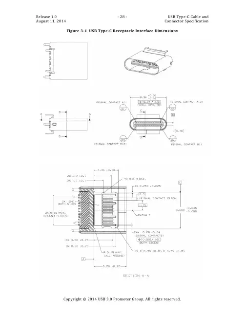
Figure 3-1 USB Type-C Receptacle Interface DimensionsFigure 3-1 USB Type-C Receptacle Interface Dimensions, cont.Figure 3-2 Reference Design USB Type-C Plug External EMC Spring Contact ZonesFigure 3-3 USB Full-Featured Type-C Plug Interface DimensionsFigure 3-4 Reference Footprint for a USB Type-C Vertical Mount Receptacle(Informative)Figure 3-5 Reference Footprint for a USB Type-C Dual-Row SMT Right AngleReceptacle (Informative)Figure 3-6 Reference Footprint for a USB Type-C Hybrid Right-Angle Receptacle(Informative)Figure 3-7 Reference Footprint for a USB Type-C Mid-Mount Dual-Row SMT Receptacle(Informative)Figure 3-8 Reference Footprint for a USB Type-C Mid-Mount Hybrid Receptacle(Informative)This specification requires that all contacts be present in the mating interface of the USB Type-C receptacle connector, but allows the plug to include only the contacts required for USB PD and USB 2.0 functionality for applications that only support USB 2.0. The USB 2.0 Type-C plug is shown in Figure 3-9. The following design simplifications may be made when only USB 2.0 is supported:∙Only the contacts necessary to support USB PD and USB 2.0 are required in the plug.All other pin locations may be unpopulated. See Table 3-5. All contacts are required to be present in the mating interface of the USB Type-C receptacle connector.∙Unlike the USB Full-Featured Type-C plug, the internal EMC springs may be formed from the same strip as the signal, power, and ground contacts. The internal EMC springs contact the inner surface of the plug shell and mate with the receptacle EMC pads when the plug is seated in the receptacle.∙ A paddle card inside the plug may not be necessary if wires are directly attac hed to the contact pins.Figure 3-9 USB 2.0 Type-C Plug Interface Dimensions3.2.2Reference DesignsThis section provides reference designs for a few key features of the USB Type-C connector. The reference designs are provided as acceptable design examples. They are not normative.3.2.2.1Receptacle Mid-Plate (Informative)The signals between the top and bottom of the receptacle tongue are isolated by a mid-plate inside the tongue. Figure 3-10 shows a reference design of the mid-plate. It is important to pay attention to the following features of the middle plate:∙The distance between the signal contacts and the mid-plate should be accurately controlled since the variation of this distance may significantly impact impedance of the connector.∙The mid-plate in this particular design protrudes slightly beyond the front surface of the tongue. This is to protect the tongue front surface from damage caused by miss-insertion of small objects into the receptacle.∙The mid-plate is required to be directly connected to the PCB ground with at least two grounding points.∙The sides of the mid-plate mate with the plug side latches, making ground connections to reduce EMC. Proper surface finishes are necessary in the areaswhere the side latches and mid-plate connections occur.Figure 3-10 Reference Design of Receptacle Mid-Plate3.2.2.2Side Latch (informative)The side latches (retention latches) are located in the plug. Figure 3-11 shows a reference design of a blanked side latch. The plug side latches should contact the receptacle mid-plate to provide an additional ground return path.Figure 3-11 Reference Design of the Retention LatchFigure 3-12 Illustration of the Latch Soldered to the Paddle Card Ground3.2.2.3Internal EMI Springs and Pads (Informative)Figure 3-13 is a reference design of the internal EMC spring located inside the USB Full-Featured Type-C plug. Figure 3-14 is a reference design of the internal EMC spring located inside the USB 2.0 Type-C plug.Figure 3-13 Reference Design of the USB Full-Featured Type-C Plug Internal EMCSpringFigure 3-14 Reference Design of the USB 2.0 Type-C Plug Internal EMC SpringIt is critical that the internal EMC spring contacts the plug shell as close to the EMC spring mating interface as possible to minimize the length of the return path.The internal EMC pad (i.e., ground plate) shown in Figure 3-15 is inside the receptacle. It mates with the EMC spring in the plug. To provide an effective ground return, the EMC pads should have multiple connections with the receptacle shell.Figure 3-15 Reference Design of Internal EMC Pad3.2.2.4Optional External Receptacle EMC Springs (Informative)Some applications may use receptacles with EMC springs that contact the outside of the plug shell. Figure 3-16 shows a reference receptacle design with external EMC springs. The EMC spring contact landing zones for the fully mated condition are normative and defined in Section 3.2.1.Figure 3-16 Reference Design of a USB Type-C Receptacle with External EMC Springs。
TYPEC数据线规格书

TYPE C数据线规格书关键词:TYPE C数据线摘要:本文介绍了数据线的规格,性能及测试规范。
缩略语:1范围标准适用于TYPE A TO C数据线需求规格书,未尽规格描述以TYPE C协会规范为准。
2编写依据3数据线正常工作和存储条件3.1数据线应能在下列条件下正常工作:工作环境温度:-20 C〜+55C;(仅作单体验证目的,与整机匹配时以整机试验环境为准);相对湿度:5%- 95%大气压力:86 kPa〜106kPa;数据线的存储温度:-40 C〜+85 C;4数据线主要参数4.1数据线连线规格详细尺寸以及工艺要求以3D图档为准1、type C 金属插头,要求必须是整体拉伸成型,不能是折弯成型,不接受接缝;2、金属插头部分,要求做不锈钢原色,表面喷砂处理:50u” ~15Ou” MATTNICKELPLATINGOVER ALL3、保证至少3A通流能力整条线缆产品详细规格(BOM青单,包括端子图纸2D &可拆解版本的3D)要有确认才能认可(认证时必须提供以上文件)。
4.2线材主体信息:4.2.1 外观5V/3A A plug TO C plug, cover 式,白色半雾面,素材细咬花处理,MT110064.2.2 主体结构绝缘材质须满足章节测试性能要求423 关键尺寸4.2.3.1 B plug参考协会规范4.2.3.2 TYPE C plug1. 红圈标示尺寸为重点尺寸,其余尺寸依据协会规范要求2. 各组件BOM LIST原材料信息需明确到具体牌号3. 应满足TYPE C规格'土-.LJ L : .:!■:.LO <4 士珂止J:T-H rcnnr|韵叮可■卜HE]*>* 八年I rn 5 > ^J1E_(PCT 閉“ fi.Q)75L jji年S" I立1 /* (1_3*平电車i ip afTg Dig *I」叶m 6 —昱己』匚JL J :.㉚:^NM r Cr3R 朋OAI『「咽吐Cl壮Hl JLC *3. dhP uhCF ^/fWT C0&-W?池;期DOUS ¥疔丁2 M烂回叫应吃笳N顶RtHJ. 和M 就皿仍it:rnns-nTEJi PCmiHt t OHM - NLU U -^CB lA VCU TIJC^E^ANCE ±0 lO^rMV9b pH]4V9K1 1■ %心iiq u r W 2QI 誑JKlLE M RUkH MU. J H1■” BU PUHI M low MJ. ui' w^i Mon -wnr.jnw nnu.1rUlLI 1■ -I3E-」■ttr E 1 厂利-«5U■:a TA~\tfb f■□£. LNLtHVirW tJMJHMI.DETAIL E4X 0.81需富(GND SPR1N6)-4X 0. 18 MIN. (T) IGND SPR1NCS<5〉间距尺寸和位査废L|2X 0^27 MIN ・ <S> (SIGNAL CONTACTS)(SIGNAL CONTACTS)• 0.0234X I .M|\.ZX 1.74 M ;H (CD絢菟尺寸<0位■/!2.80 :0.0&(RtTCMf ION SWINGS 〉L<C 751I^IONAL C0N1ACT PITCH)HA -.IU r:心 t 0.250 xo-oeoDRCLTO SPRINGSCO >36}SECTION A AQ AND BOTTOM CONTACTS SHALL NOT TOUCH间距尺寸和位Jtt 度(0,25 M[N,I5PARP EDGES ARE NOT PEAM1S5:B_ERAD]US OR 匚HAMFER ALL AROUND REQUIREDSECTION OC423.3 镀层厚度测试区域规定关于镀层测试区域和方法:TYPEC/A : TYPEC/A 产生接触的关键区域为PIN 针头部触点,因此镀层工艺为考虑成本一般只覆盖PIN 针触点位置,其他区域为 flash Au,所以镀层的量测范围定义在PIN 针触点弧顶的最高处< Af 镀层厚度为在触点弧 、顶最高点的范围内进行测量,同一触点在 范围内测量三次取平 均值DETAIL G-6.6匕 ±0.】0ZX 1.570 +0.0Z5:-0*800 *0.025I TONGUE OPENING!I ・ 3C0 tO.O25T A T RZX C C ・]d ±0・05 X ^5*(BOTH SIDES7424 线序Table 3-20 USBType-C to USB AMWiringUSB Type-C PlugUSB AMPin Signal Name Pin Signal NameA1, B1, A12, B12 GND 4 GNDA4, B4, A9, B9 VBUS 1 VBUSA5 CCA6 Dpi 3 D+A7 Dni 2 DShell Shield Shell ShieldNotes:1. Pin A5 (CC) of the USBType-C plug shall be connected to V BUs through a resistor Rp. See Section and Table 4-13 for the functional description and value of Rp.2. Contacts B6 and B7 should not be present in the USB Type-C plug.3. All V BUS pins shall be connected together within the USB Type-C plug. Bypass capacitors are notrequired for the V BUS pins at this cable.4. All Ground return pins shall be connected together within the USB Type-C plug.5. All USB Type-C plug pins that are not listed in this table shall be open (not connected).Standard-A plug QMicro-B receptacle <-'Table 4-13 DFP CC Term in ati on (Rp) Requireme nts DFP Advertiseme nt Curre nt Source to-VResistor pull-up to-VResistor pull-up toV 士5%Default USB Power 80 A ± 20% 56 k Q 士 20%(Note 1) 36 k Q 士20%A @ 5 V 180 卩 A ± 8% 22 k Q 士5% 12 k Q 士5%A @ 5 V 330 卩A ± 8% 10 k Q 士5% k Q 士5%Notes:DRP5技术要求5.1 线材外观要求5.1.1 线材外观要求如下:未尽事宜参考《》5.2 线材性能要求Test con diti onTemperature : 15C to 35 °CAir pressure : 86 to106 kPaRelative humidity : 25% to 85%5.3 安全性要求USB数据线的安全性能应能满足CCEE规定要求。
USB Type-C 规范1.2(中文版)

知识产权声明
THIS SPECIFICATION IS PROVIDED TO YOU “AS IS” WITH NO WARRANTIES WHATSOEVER, INCLUDING ANY WARRANTY OF MERCHANTABILITY, NON-INFRINGEMENT, OR FITNESS FOR ANY PARTICULAR PURPOSE. THE AUTHORS OF THIS SPECIFICATION DISCLAIM ALL LIABILITY, INCLUDING LIABILITY FOR INFRINGEMENT OF ANY PROPRIETARY RIGHTS, RELATING TO USE OR IMPLEMENTATION OF INFORMATION IN THIS SPECIFICATION. THE PROVISION OF THIS SPECIFICATION TO YOU DOES NOT PROVIDE YOU WITH ANY LICENSE, EXPRESS OR IMPLIED, BY ESTOPPEL OR OTHERWISE, TO ANY INTELLECTUAL PROPERTY RIGHTS.
预发行行业审查公司提供反馈
Revision History.......................................................................................................................14
LIMITED COPYRIGHT LICENSE: The USB 3.0 Promoters grant a conditional copyright license under the copyrights embodied in the USB Type-C Cable and Connector Specification to use and reproduce the Specification for the sole purpose of, and solely to the extent necessary for, evaluating whether to implement the Specification in products that would comply with the specification.
usb,type,c,协会规范

竭诚为您提供优质文档/双击可除usb,type,c,协会规范篇一:usb3.1type-c公对公接点图usb3.1(type-c)接点图usb3.1type-c公对公接点图pin的四种类型:1、usb3.1中Rx、tx为高速pin;2、usb2.0数据pin;3、边频带信号pin;4、电源及地线pin.图表中a6,a7为usb2.0的数据pin;a8,b8为预留pin;a5,b5为配置通道或有源器件电源;配置通道的功能:1、探测usbtypec连接器端口是否插配,从而决定如何配置电源的供应;2、探测usbtypec公头连接器的方向性,从而决定采用哪侧的高速信号pin组传输信号;3、建立连接的主从关系;4、探测连接的额电流水平/大小,控制或配置电源的供应水平;5、usbpd通讯;6、给有源器件供应电源;7、功能延伸。
usbtypec连接器-公头设计指南:使用高性能的pcb基板材料。
推荐pcb厚度应该有一个公差小于或等于±10%的usb插针间距;篇二:typec数据线规格书typec数据线规格书V1.0关键词:typec、数据线摘要:本文介绍了数据线的规格,性能及测试规范。
缩略语:1范围标准适用于typeatoc数据线需求规格书,未尽规格描述以typec协会规范V1.1为准。
2编写依据3数据线正常工作和存储条件3.1数据线应能在下列条件下正常工作:3.1.1工作环境温度:-20℃~+55℃;(仅作单体验证目的,与整机匹配时以整机试验环境为准);3.1.2相对湿度:5%~95%;3.1.3大气压力:86kpa~106kpa;3.1.4数据线的存储温度:-40℃~+85℃;4数据线主要参数4.1数据线连线规格详细尺寸以及工艺要求以3d图档为准1、typec金属插头,要求必须是整体拉伸成型,不能是折弯成型,不接受接缝;2、金属插头部分,要求做不锈钢原色,表面喷砂处理:50u”~150u”mattnickelplatingoVeRall3、保证至少3a通流能力整条线缆产品详细规格(bom清单,包括端子图纸2d&可拆解版本的3d)要有确认才能认可(认证时必须提供以上文件)。
type-c的标准
type-c的标准Type-C接口是一种通用、高效的数据传输和充电接口,逐渐被广泛应用在各种电子设备上。
为了保障产品的质量和可靠性,必须对Type-C接口进行严格的寿命插拔测试。
以下是Type-C接口的一些主要标准:1. 接触电阻:接触电阻是评估Type-C接口性能的重要指标之一。
在插拔测试过程中,需要详细记录每次插拔后的接口状态,包括接触电阻、插拔力等数据。
合格的Type-C母座的接触电阻应该在一定范围内,一般小于50mΩ,以确保良好的电气连接和信号传输质量。
2. 插拔寿命:Type-C接口寿命插拔测试的主要目的是评估接口在多次插拔过程中的耐用性和稳定性。
测试过程中需要模拟用户在实际使用过程中的插拔行为,检测接口在长时间使用下是否容易出现磨损、松动、接触不良等问题。
一般需要进行数千次甚至数万次的插拔测试。
3. 插拔速度:在测试过程中,需要模拟用户在实际使用过程中的插拔速度,避免过快或过慢的插拔行为,以确保测试结果的准确性。
4. 结构测试:包括耐插拔寿命试验、线缆弯曲试验、线缆拔出试验、4轴向测试等,以评估Type-C接口在不同使用场景下的性能和稳定性。
5. 电气测试:包括低电平接触电阻测试、电流温升测试、绝缘电阻、耐电压、接触电容、阻抗等,以评估Type-C接口的电气性能。
6. 环境测试:包括物理冲击、任意振动、热冲击、腐蚀气体冲击、温湿度老化等,以评估Type-C接口在不同环境下的可靠性和稳定性。
7. 电镀要求:包括可焊性、抗潮性、耐腐蚀性等,以确保Type-C 接口在使用过程中的质量和性能。
8. 屏蔽测试:线材屏蔽的好坏将影响到EMI与RFI,USB协会针对线材屏蔽的测试也定义了严谨的测试要求。
9. 高频测试:上述高频测试完成后,ILfitatNq、IMR、INEXT、IFEXT、IRL这5项参数必须通过USB协会所公告的公式进行换算,才能得知此Type-C线缆是否符合协会的要求。
综上所述,Type-C接口的标准包括接触电阻、插拔寿命、插拔速度、结构测试、电气测试、环境测试、电镀要求、屏蔽测试和高频测试等多个方面。
TYPE C数据线规格书
TYPE C数据线规格书关键词:TYPE C、数据线摘要:本文介绍了数据线的规格,性能及测试规范。
缩略语:1范围标准适用于 TYPE A TO C数据线需求规格书,未尽规格描述以TYPE C协会规范为准。
2编写依据3数据线正常工作和存储条件3.1数据线应能在下列条件下正常工作:工作环境温度:-20℃~+55℃;(仅作单体验证目的,与整机匹配时以整机试验环境为准);相对湿度:5%~95%;大气压力:86 kPa~106kPa;数据线的存储温度:-40℃~+85℃;4数据线主要参数4.1数据线连线规格详细尺寸以及工艺要求以3D图档为准1、 type C金属插头,要求必须是整体拉伸成型,不能是折弯成型,不接受接缝;2、金属插头部分,要求做不锈钢原色,表面喷砂处理: 50u”~150u”MATT NICKEL PLATING OVER ALL3、保证至少3A通流能力整条线缆产品详细规格(BOM清单, 包括端子图纸2D & 可拆解版本的3D)要有确认才能认可(认证时必须提供以上文件)。
4.2线材主体信息:4.2.1外观5V/3A A plug TO C plug, cover式,白色半雾面,素材细咬花处理,MT110064.2.2主体结构导体材质规格如下:材质:镀锡铜绝缘材质NON-PVC,须满足章节测试性能要求4.2.3关键尺寸4.2.3.1 B plug参考协会规范4.2.3.2TYPE C plug1.红圈标示尺寸为重点尺寸,其余尺寸依据协会规范要求2.各组件BOM LIST原材料信息需明确到具体牌号3.应满足TYPE C 规格4.2.3.3镀层厚度测试区域规定关于镀层测试区域和方法:TYPE C/A:TYPE C/A 产生接触的关键区域为PIN针头部触点,因此镀层工艺为考虑成本一般只覆盖PIN针触点位置,其他区域为flash Au,所以镀层的量测范围定义在PIN针触点弧顶的最高处5技术要求5.1线材外观要求5.1.1线材外观要求如下:未尽事宜参考《终端数据线检验通用操作指导书》5.2线材性能要求Test conditionTemperature:15℃ to 35℃Air pressure :86 to106 kPaRelative humidity:25% to 85%以插入力和拔出力测试标准为依据,测试TYPE C端子插拔次数10000次(正反方向各5000次,每2500次换一个方向)做完25次插拔之后,插拔力变化不能超过33%A公插拔1500次测试结束后端子外观无异常、插拔力需要满足要求插拔耐久测试前后:Type C:插入力5~20N ;USB AM: 35N(MAX)插拔耐久测试前后:Type C:拔出力8~20NUSB AM: 10N(Min)测试后,样品外观、机械结构应正常,功能和电气性能正应常的上下左右4个方向力量要求大于,插入方向要求大于10Kg,连接器不允许有失效,接口允许有可恢复的变形,数据线电气性能正常;结构无松脱,无断裂两端壳体都需要测试抗拉脱力,测试后两端壳体不应有脱落现象数据线外观结构、功能及电气性能应正常,端子不应有损坏或严重变形Type C /B plug Plating gold Au 不小于30µ″,Plating Ni 不小于 80µ″认证测试:100VAC/60s/产线测试:100VAC/认证测试: 300VDC 60s 100MΩ产线测试:300VDC/10MΩ部品外观无损坏;线缆电气性能正常样品外观无损坏;线缆电气性能正常测试后,样品外观、机械结构应正常,功能和电气性能应正常试验后,样品外观应无明显锈蚀、变色、及镀层剥落等现象。
Type C协会标准规范
Coupling between VBus and differential USB D+/D-
≦-40dB for 0.3MHz<f≦ 30MHz, and ≦
19.12log10(f/30)-40(in dB) for 30MHz<f≦ 100MHz
Single-ended coupling between SBU_A and CC,
SBU_B and CC
Single-ended coupling between CC and D-
The limit is defined with the vertices of
(0.3MHz, -65dB), (1MHz, -55dB), (18MHz, -30dB), and (100MHz, -
25dB) in scale of log10(f)
The limit is defined with the vertices of
(0.3MHz, -80dB), (30MHz, -40dB) and (100MHz, -40dB) in scale of log10(f)
≦ 900 nH
Vbus capacitance
Group B-1 Type C connector and cable assembly mechanical tests
Cable pull out 線材吊重
協會標準 40 N Minmum, 線材組裝 需無電性斷開且線材不會
從CONN分離
Cable flex 線材柔軟
No loss of continuity during cycling
Single-ended coupling between SBU_A and SBU_B
type c协会认证流程
type c协会认证流程
USB Type-C的认证流程主要包括以下步骤:
1. 提交申请:向USB协会提交申请,并支付相应的费用。
2. 产品检测:将产品送到指定的检测机构进行检测,检测内容包括但不限于产品的电气性能、物理尺寸、材料等。
3. 认证审核:USB协会对检测机构提交的检测报告进行审核,确认产品是否符合USB Type-C的标准。
4. 认证通过:如果产品通过了检测和审核,USB协会会授予认证证书,并允许在产品上使用USB Type-C的标识。
需要注意的是,具体的认证流程可能会因为不同的产品、不同的标准而有所不同。
因此,在进行Type-C认证时,建议先了解相关的标准和规定,并咨询专业机构或USB协会的相关工作人员。