ISL6754EVAL2Z 1600W ZVS DC
ISL8487EIB中文资料
1
CAUTION: These devices are sensitive to electrostatic discharge; follow proper IC Handling Procedures. 1-888-INTERSIL or 1-888-468-3774 | Intersil (and design) is a registered trademark of Intersil Americas Inc. Copyright © Intersil Americas Inc. 2003-2005. All Rights Reserved All other trademarks mentioned are the property of their respective owners.
*Shutdown Mode for ISL8487E, ISL81487L (See Note 7)
TABLE 1. SUMMARY OF FEATURES PART NUMBER ISL8487E ISL81487L ISL81487E HALF/FULL DUPLEX Half Half Half NO. OF DEVICES DATA RATE ALLOWED ON BUS (Mbps) 256 256 256 0.25 0.25 5 SLEW-RATE LIMITED? Yes Yes No RECEIVER/ QUIESCENT LOW POWER PIN DRIVER ENABLE? ICC (µA) SHUTDOWN? COUNT Yes Yes Yes 120 120 350 Yes Yes No 8 8 8
*Shutdown Mode for ISL8487E, ISL81487L (See Note 7) RECEIVING INPUTS RE 0 0 0 1 1 DE 0 0 0 0 1 A-B ≥ +0.2V ≤ -0.2V Inputs Open X X OUTPUT RO 1 0 1 High-Z * High-Z
IR公司_大功率MOS管选型

I DContinuous Drain Current(A)70°Micro3Surface Mount PackagesV (BR)DSSDrain-to-Source Breakdown Voltage (V)R DS(on)On-State Resistance ()ΩI D Continuous Drain Current 25°C(A)R ΘMax.Thermal Resistance (°C/W)1FaxonDemand Number Case Outline KeyPartNumberPD Max.PowerDissipation (W)N-ChannelLogic LevelIRLML2402*912570.54200.25 1.20.95230H1IRLML2803912580.54300.251.20.93230P-ChannelLogic LevelIRLML6302*912590.54-200.6-0.62-4.8230H1IRLML5103912600.54-300.6-0.61-4.8230* Indicates low VGS(th), which can operate at VGS = 2.7VMeasured at ambient for Micro3, Micro6, Micro8, SO-8, and SOT-223 package styles. All others measured at case.1Micro3SO-8D-PakD -PakSOT-227Micro6SOT-223Micro82 Illustrations not to scaleI DContinuous Drain Current(A)70°Micro6Surface Mount PackagesV (BR)DSSDrain-to-Source Breakdown Voltage (V)R DS(on)On-State Resistance ()ΩI D Continuous Drain Current 25°C(A)R ΘMax.Thermal Resistance (°C/W)1FaxonDemand Number Case Outline KeyPartNumberPD Max.PowerDissipation (W)N-ChannelLogic LevelIRLMS1902915401.7200.10 3.2 2.675H2IRLMS1503915081.7300.103.22.675P-ChannelLogic LevelIRLMS6702*914141.7-200.20-2.3-1.975H2IRLMS5703914131.7-300.20-2.3-1.975* Indicates low VGS(th), which can operate at VGS = 2.7VMeasured at ambient for Micro3, Micro6, Micro8, SO-8, and SOT-223 package styles. All others measured at case.1Micro3SO-8D-PakD -PakSOT-227Micro6SOT-223Micro82 Illustrations not to scaleI DContinuous Drain Current(A)70°Micro8Surface Mount PackagesV (BR)DSSDrain-to-Source Breakdown Voltage (V)R DS(on)On-State Resistance ()ΩI D Continuous Drain Current 25°C(A)R ΘMax.Thermal Resistance (°C/W)1FaxonDemand Number Case Outline KeyPart NumberP D Max.PowerDissipation (W)N-Channel Logic LevelIRF7601* 912611.820 0.035 5.7 4.6 70 H3IRF7603 912621.830 0.035 5.6 4.5 70Dual N-Channel Logic LevelIRF7501* 912651.220 0.135 2.4 1.9 100 H3IRF7503 912661.2530 0.135 2.4 1.9 100P-Channel Logic LevelIRF7604* 912631.8-20 0.09 -3.6 -2.9 70 H3IRF7606 912641.8-30 0.09 -3.6 -2.9 70Dual P-Channel Logic LevelIRF7504* 912671.25-20 0.27 -1.7 -1.4 100 H3IRF7506 912681.25-30 0.27 -1.7 -1.4 100Dual N- and P-Channel Logic LevelIRF7507* 912691.2520 0.1352.4 1.9 100 H3-20 0.27 -1.7 -1.4IRF7509 912701.2530 0.135 2.4 1.9 100-30 0.27 -1.7 -1.4* Indicates low VGS(th), which can operate at VGS = 2.7VMeasured at ambient for Micro3, Micro6, Micro8, SO-8, and SOT-223 package styles. All others measured at case.1Micro3SO-8D-Pak D -PakSOT-227Micro6SOT-223Micro8 2 Illustrations not to scaleI DContinuous Drain Current(A)70°SO-8Surface Mount PackagesV (BR)DSSDrain-to-Source Breakdown Voltage (V)R DS(on)On-State Resistance ()ΩI D Continuous Drain Current 25°C(A)R ΘMax.Thermal Resistance (°C/W)1FaxonDemand Number Case Outline KeyPart Number P D Max.PowerDissipation (W)N-ChannelIRF7413913302.5300.011139.250H4IRF7413A 916132.5300.0135128.450IRF9410915622.5300.0375.850Dual N-ChannelIRF7311914352.0200.029 6.6 5.362.5H4IRF7313914802.0300.029 6.5 5.262.5IRF7333917002.0300.10 3.5 2.862.5917002.0300.050 4.9 3.962.5IRF9956915592.0300.103.52.862.5Dual P-ChannelIRF7314914352.0-200.058-5.3-4.362.5H4IRF7316915052.0-300.058-4.9-3.962.5IRF9953915602.0-300.25-2.3-1.862.5* Indicates low VGS(th), which can operate at VGS = 2.7VMeasured at ambient for Micro3, Micro6, Micro8, SO-8, and SOT-223 package styles. All others measured at case.1Micro3SO-8D-PakD -PakSOT-227Micro6SOT-223Micro82 Illustrations not to scaleI DContinuous Drain Current(A)70°SO-8Surface Mount PackagesV (BR)DSSDrain-to-Source Breakdown Voltage (V)R DS(on)On-State Resistance ()ΩI D Continuous Drain Current 25°C(A)RΘMax.ThermalResistance(°C/W)1FaxonDemand Number Case Outline KeyPart NumberP D Max.PowerDissipation (W)Dual N- and P-ChannelIRF7317 915682.020 0.029 6.6 5.3 62.5 H42.0-20 0.058 -5.3 -4.3 62.5IRF9952 915622.030 0.103.5 2.8 62.5915622.0-30 0.25 -2.3 -1.8 62.5IRF7319 916062.030 0.029 6.5 5.2 62.52.0-30 0.058 -4.9 -3.9 62.5* Indicates low VGS(th), which can operate at VGS = 2.7VMeasured at ambient for Micro3, Micro6, Micro8, SO-8, and SOT-223 package styles. All others measured at case.1Micro3SO-8D-Pak D -PakSOT-227Micro6SOT-223Micro8 2 Illustrations not to scaleI DContinuous Drain Current(A)70°SO-8Surface Mount PackagesV (BR)DSSDrain-to-Source Breakdown Voltage (V)R DS(on)On-State Resistance ()ΩI D Continuous Drain Current 25°C(A)R ΘMax.Thermal Resistance (°C/W)1FaxonDemand Number Case Outline KeyPart Number P D Max.PowerDissipation (W)N-ChannelLogic LevelIRF7401912442.5200.0228.77.050H4IRF7201911002.5300.0307.0 5.650IRF7403912452.5300.0228.55.450Dual N-ChannelLogic LevelIRF7101908712.0200.10 3.5 2.362.5H4IRF7301912382.0200.050 5.2 4.162.5IRF7303912392.0300.050 4.9 3.962.5IRF7103910952.0500.1303.02.362.5P-ChannelLogic LevelIRF7204911032.5-200.060-5.3-4.250H4IRF7404912462.5-200.040-6.7-5.450IRF7205911042.5-300.070-4.6-3.750IRF7406912472.5-300.045-5.8-3.750IRF7416913562.5-300.02-10-7.150* Indicates low VGS(th), which can operate at VGS = 2.7VMeasured at ambient for Micro3, Micro6, Micro8, SO-8, and SOT-223 package styles. All others measured at case.1Micro3SO-8D-PakD -PakSOT-227Micro6SOT-223Micro82 Illustrations not to scaleI DContinuous Drain Current(A)70°SO-8Surface Mount PackagesV (BR)DSSDrain-to-Source Breakdown Voltage (V)R DS(on)On-State Resistance ()ΩI D Continuous Drain Current 25°C(A)R ΘMax.Thermal Resistance (°C/W)1FaxonDemand Number Case Outline KeyPart Number P D Max.PowerDissipation (W)Dual P-ChannelLogic LevelIRF7104910962.0-200.250-2.3-1.862.5H4IRF7304912402.0-200.090-4.3-3.462.5IRF7306912412.0-300.10-3.6-2.962.5Dual N- and P-Channe Logic LevelIRF7307912421.4200.050 4.3 3.490H4-200.090-3.6-2.9IRF7105910972.0250.1093.5 2.862.52-250.25-2.3-1.862IRF7309912432.0300.050 4.9 3.962.5-300.10-3.6-2.9* Indicates low VGS(th), which can operate at VGS = 2.7VMeasured at ambient for Micro3, Micro6, Micro8, SO-8, and SOT-223 package styles. All others measured at case.1Micro3SO-8D-PakD -PakSOT-227Micro6SOT-223Micro82 Illustrations not to scaleI DContinuous Drain Current(A)70°SOT-223Surface Mount PackagesV (BR)DSSDrain-to-Source Breakdown Voltage (V)R DS(on)On-State Resistance ()ΩI D Continuous Drain Current 25°C(A)R ΘMax.Thermal Resistance (°C/W)1FaxonDemand Number Case Outline KeyPart Number P D Max.PowerDissipation (W)N-ChannelIRFL4105913812.1550.045 3.7 3.060H6IRFL110908612.01000.54 1.50.9660IRFL4310913682.11000.20 1.6 1.360IRFL21090868 2.02001.50.960.660IRFL214908622.02502.00.790.560P-ChannelIRFL9110908642.0-1001.2-1.1-0.6960H6N-ChannelLogic LevelIRLL3303913792.1300.031 4.6 3.760H6IRLL014N 914992.1550.14 2.0 1.660IRLL2705913802.1550.043.83.060* Indicates low VGS(th), which can operate at VGS = 2.7VMeasured at ambient for Micro3, Micro6, Micro8, SO-8, and SOT-223 package styles. All others measured at case.1Micro3SO-8D-PakD -PakSOT-227Micro6SOT-223Micro82 Illustrations not to scaleI DContinuous Drain Current(A)100°D-PakSurface Mount PackagesV (BR)DSSDrain-to-Source Breakdown Voltage (V)R DS(on)On-State Resistance ()ΩI D Continuous Drain Current 25°C(A)R ΘMax.Thermal Resistance (°C/W)1FaxonDemand Number Case Outline KeyPart Number P D Max.PowerDissipation (W)N-ChannelIRFR33039164257300.0313321 2.2H7IRFR024N9133638550.0751610 3.3IRFR41059130248550.0452516 2.7IRFR12059131869550.0273723 1.8IRFR11090524251000.54 4.3 2.75IRFR120N 91365391000.219.1 5.8 3.2IRFR391091364521000.11159.5 2.4IRFR2109052625200 1.5 2.6 1.75IRFR22090525422000.8 4.833IRFR21490703252502 2.2 1.45IRFR2249060042250 1.1 3.8 2.43IRFR3109059725400 3.6 1.7 1.15IRFR3209059842400 1.8 3.123IRFR42090599425003 2.4 1.53IRFRC2090637426004.421.33* Indicates low VGS(th), which can operate at VGS = 2.7VMeasured at ambient for Micro3, Micro6, Micro8, SO-8, and SOT-223 package styles. All others measured at case.1Micro3SO-8D-PakD -PakSOT-227Micro6SOT-223Micro82 Illustrations not to scaleI DContinuous Drain Current(A)100°D-PakSurface Mount PackagesV (BR)DSSDrain-to-Source Breakdown Voltage (V)R DS(on)On-State Resistance ()ΩI D Continuous Drain Current 25°C(A)R ΘMax.Thermal Resistance (°C/W)1FaxonDemand Number Case Outline KeyPart Number P D Max.PowerDissipation (W)P-ChannelIRFR55059161057-550.11-18-11 2.2H7IRFR53059140289-550.065-28-18 1.4IRFR90149065425-600.5-5.1-3.25IRFR90249065542-600.28-8.8-5.63IRFR91109051925-100 1.2-3.1-25IRFR91209052042-1000.6-5.6-3.63IRFR9120N 9150739-1000.48-6.5-4.1 3.2IRFR92109052125-2003-1.9-1.25IRFR92209052242-200 1.5-3.6-2.33IRFR92149165850-250 3.0-2.7-1.7 2.5IRFR93109166350-4007.0-1.8-1.12.5* Indicates low VGS(th), which can operate at VGS = 2.7VMeasured at ambient for Micro3, Micro6, Micro8, SO-8, and SOT-223 package styles. All others measured at case.1Micro3SO-8D-PakD -PakSOT-227Micro6SOT-223Micro82 Illustrations not to scaleI DContinuous Drain Current(A)100°D-PakSurface Mount PackagesV (BR)DSSDrain-to-Source Breakdown Voltage (V)R DS(on)On-State Resistance ()ΩI D Continuous Drain Current 25°C(A)R ΘMax.Thermal Resistance (°C/W)1FaxonDemand Number Case Outline KeyPart Number P D Max.PowerDissipation (W)N-ChannelLogic LevelIRLR27039133538300.0452214 3.3H7IRLR33039131657300.0313321 2.2IRLR31039133369300.0194629 1.8IRLR024N 9136338550.0651711 3.3IRLR27059131746550.042415 2.7IRLR29059133469550.0273623 1.8IRLR120N 91541391000.18511 6.9 3.2IRLR341091607521000.10159.52.4* Indicates low VGS(th), which can operate at VGS = 2.7VMeasured at ambient for Micro3, Micro6, Micro8, SO-8, and SOT-223 package styles. All others measured at case.1Micro3SO-8D-PakD -PakSOT-227Micro6SOT-223Micro82 Illustrations not to scaleI DContinuous Drain Current(A)100°D 2PakSurface Mount PackagesV (BR)DSSDrain-to-Source Breakdown Voltage (V)R DS(on)On-State Resistance ()ΩI D Continuous Drain Current 25°C(A)R ΘMax.Thermal Resistance (°C/W)1FaxonDemand Number Case Outline KeyPart NumberP D Max.PowerDissipation (W)N-ChannelIRFZ24NS 913554555 0.07 17 12 3.3 H10IRFZ34NS 913116855 0.04 29 20 2.2IRFZ44NS 9131511055 0.022 49 35 1.4IRFZ46NS 9130512055 0.020 53 37 1.3IRFZ48NS 9140814055 0.016 64 45 1.1IRF1010NS 913723.855 0.011 84 60 40IRF3205S 9130420055 0.008 110 80 0.75IRFZ44ES 9171411060 0.023 48 34 1.4IRF1010ES 9172017060 0.012 83 59 0.90IRF2807S 9151815075 0.013 71 50 1.0IRF520NS 9134047100 0.2 9.5 6.7 3.2IRF530NS 9135263100 0.11 15 11 2.4IRF540NS 91342110100 0.052 27 19 1.6IRF1310NS 91514120100 0.036 36 25 1.3IRF3710S 91310150100 0.028 46 33 1.0IRF3315S 9161794150 0.082 21 15 1.6IRF3415S 91509150150 0.042 37 26 1.0IRFBC20S 9.101450600 4.4 2.2 1.4 2.5IRFBC30S 9101574600 2.2 3.6 2.3 1.7IRFBC40S 91016130600 1.2 6.2 3.9 1.0* Indicates low VGS(th), which can operate at VGS = 2.7VMeasured at ambient for Micro3, Micro6, Micro8, SO-8, and SOT-223 package styles. All others measured at case.1Micro3SO-8D-Pak D -PakSOT-227Micro6SOT-223Micro8 2 Illustrations not to scaleI DContinuous Drain Current(A)100°D 2PakSurface Mount PackagesV (BR)DSSDrain-to-Source Breakdown Voltage (V)R DS(on)On-State Resistance ()ΩI D Continuous Drain Current 25°C(A)R ΘMax.Thermal Resistance (°C/W)1FaxonDemandNumberCase Outline KeyPart NumberP D Max.PowerDissipation (W)IRFBF20S 9166554900 8.0 1.7 1.1 2.3 H10P-ChannelIRF5305S 91386110-55 0.06 -31 -22 1.4 H10IRF4905S 914783.8-55 0.02 -74 -52 40IRF9520NS 9152247-100 0.48 -6.7 -4.8 3.2IRF9530NS 9152375-100 0.20 -14 -9.9 2.0IRF9540NS 9148394-100 0.117 -19 -13 1.6IRF5210S 91405150-100 0.06 -35 -25 1.0* Indicates low VGS(th), which can operate at VGS = 2.7VMeasured at ambient for Micro3, Micro6, Micro8, SO-8, and SOT-223 package styles. All others measured at case.1Micro3SO-8D-Pak D -PakSOT-227Micro6SOT-223Micro8 2 Illustrations not to scaleI DContinuous Drain Current(A)100°D 2PakSurface Mount PackagesV (BR)DSSDrain-to-Source Breakdown Voltage (V)R DS(on)On-State Resistance ()ΩI D Continuous Drain Current 25°C(A)R ΘMax.Thermal Resistance (°C/W)1FaxonDemand Number Case Outline KeyPart NumberP D Max.PowerDissipation (W)N-Channel Logic LevelIRL3302S 916925720 0.020 39 25 2.2 H10IRL3202S916756920 0.016 48 30 1.8IRL3102S 916918920 0.013 61 39 1.4IRL3402S 9169311020 0.01 85 54 1.1IRL3502S 9167614020 0.007 110 67 0.89IRL2703S 913604530 0.04 24 17 3.3IRL3303S 913236830 0.026 38 27 2.2IRL3103S 9133811030 0.014 64 45 1.4IRL2203NS 9136717030 0.007 116 82 0.90IRL3803S 9131920030 0.006 140 98 0.75IRLZ24NS 913584555 0.06 18 13 3.3IRLZ34NS 913086855 0.035 30 21 2.2IRLZ44NS 9134711055 0.022 47 33 1.4IRL3705NS 9150217055 0.01 89 63 0.90IRL2505S 9132620055 0.008 104 74 0.75IRLZ44S 9090615060 0.028 50 36 1.0IRL530NS 9134963100 0.1 15 11 2.4IRL2910S 91376150100 0.026 48 34 1.0* Indicates low VGS(th), which can operate at VGS = 2.7VMeasured at ambient for Micro3, Micro6, Micro8, SO-8, and SOT-223 package styles. All others measured at case.1Micro3SO-8D-Pak D -PakSOT-227Micro6SOT-223Micro8 2 Illustrations not to scaleI DContinuous Drain Current(A)100°SOT-227Surface Mount PackagesV (BR)DSSDrain-to-Source Breakdown Voltage (V)R DS(on)On-State Resistance ()ΩI D Continuous DrainCurrent 25°C(A)RΘMax.Thermal Resistance (°C/W)1FaxonDemand Number Case Outline KeyPart Number P D Max.PowerDissipation (W)N-ChannelFully Isolated Low ChargeFA38SA50LC 916155005000.1338240.25H21FA57SA50LC916506255000.0857360.20* Indicates low VGS(th), which can operate at VGS = 2.7VMeasured at ambient for Micro3, Micro6, Micro8, SO-8, and SOT-223 package styles. All others measured at case.1Micro3SO-8D-PakD -PakSOT-227Micro6SOT-223Micro82 Illustrations not to scaleI DContinuous Drain Current(A)100°I-PakThrough-Hole PackagesV (BR)DSSDrain-to-Source Breakdown Voltage (V)R DS(on)On-State Resistance ()ΩI D Continuous Drain Current 25°C(A)R ΘMax.Thermal Resistance (°C/W)1FaxonDemand Number Case Outline KeyPart Number P D Max.PowerDissipation (W)N-ChannelIRFU33039164257300.0313321 2.2H8IRFU024N 9133638550.0751610 3.3IRFU41059130248550.0452519 2.7IRFU12059131869550.0273723 1.8IRFU11090524251000.54 4.3 2.7 5.0IRFU120N 91365391000.219.1 5.8 3.2IRFU391091364521000.11159.5 2.4IRFU2109052625200 1.5 2.6 1.7 5.0IRFU22090525422000.80 4.8 3.0 3.0IRFU2149070325250 2.0 2.2 1.4 5.0IRFU2249060042250 1.1 3.8 2.4 3.0IRFU3109059725400 3.6 1.7 1.1 5.0IRFU3209059842400 1.8 3.1 2.0 3.0IRFU4209059942500 3.0 2.4 1.5 3.0IRFUC2090637426004.42.01.33.0I-PakTO-220 FullPakTO-262TO-247HEXDIPTO-220AB Illustrations not to scale** Not ratedI DContinuous Drain Current(A)100°I-PakThrough-Hole PackagesV (BR)DSSDrain-to-Source Breakdown Voltage (V)R DS(on)On-State Resistance ()ΩI D Continuous Drain Current 25°C(A)R ΘMax.Thermal Resistance (°C/W)1FaxonDemand Number Case Outline KeyPart Number P D Max.PowerDissipation (W)P-ChannelIRFU55059161057-550.11-18-11 2.2H8IRFU53059140289-550.065-28-18 1.4IRFU90149065425-600.50-5.1-3.2 5.0IRFU90249065542-600.28-8.8-5.6 3.0IRFU91109051925-100 1.2-3.1-2.0 5.0IRFU91209052042-1000.60-5.6-3.6 3.0IRFU9120N 9150739-1000.48-6.5-4.1 3.2IRFU92109052125-200 3.0-1.9-1.2 5.0IRFU92209052242-200 1.5-3.6-2.3 3.0IRFU92149165850-2503.0-2.7-1.7 2.5IRFU93109166350-4007.0-1.8-1.12.5N-ChannelLogic LevelIRLU27039133538300.0452214 3.3H8IRLU33039131657300.0313321 2.2IRLU31039133369300.0194629 1.8IRLU024N 9136338550.0651711 3.3IRLU27059131746550.04241715IRLU29059133469550.0273623 1.8IRLU120N 91541391000.18511 6.9 3.2IRLU341091607521000.10159.52.4I-PakTO-220 FullPakTO-262TO-247HEXDIPTO-220AB Illustrations not to scale** Not ratedI DContinuous Drain Current(A)100°HEXDIPThrough-Hole PackagesV (BR)DSSDrain-to-Source Breakdown Voltage (V)R DS(on)On-State Resistance ()ΩI D Continuous Drain Current 25°C(A)R ΘMax.Thermal Resistance (°C/W)1FaxonDemand Number Case Outline KeyPart Number P D Max.PowerDissipation (W)N-ChannelIRFD014907001.3600.2 1.7 1.2120H9IRFD024906991.3600.1 2.5 1.8120IRFD110903281.31000.54 1.00.71120IRFD120903851.31000.27 1.30.94120IRFD210903861.3200 1.50.60.38120IRFD220904171.32000.80.80.50120IRFD214912711.3250 2.00.570.32120IRFD224912721.3250 1.10.760.43120IRFD310912251.3400 3.60.420.23120IRFD320912261.3400 1.80.600.33120IRFD420912271.3500 3.00.460.26120IRFDC20912281.36004.40.320.21120I-PakTO-220 FullPakTO-262TO-247HEXDIPTO-220AB Illustrations not to scale** Not ratedI D Continuous Drain Current (A)100°TO-220Qg TotalGate Charge(nC)Through-Hole PackagesV (BR)DSSDrain-to-Source Breakdown Voltage (V)R DS(on)On-State Resistance ()ΩI D Continuous Drain Current 25°C (A)R ΘMax.Thermal Resistance(°C/W)1Faxon Demand Number Case OutlineKeyPart Number P D Max.Power Dissipation (W)N-ChannelLow ChargeIRF737LC91314743000.75 6.1** 1.7 3.9H11IRF740LC 910681254000.5510** 1.039IRF840LC 910691255000.858.0** 1.039IRFBC40LC910701256001.26.2**1.039I-PakTO-220 FullPakTO-262TO-247HEXDIPTO-220AB Illustrations not to scale** Not ratedI DContinuous Drain Current(A)100°TO-220ABThrough-Hole PackagesV (BR)DSSDrain-to-Source Breakdown Voltage (V)R DS(on)On-State Resistance ()ΩI D Continuous Drain Current 25°C(A)R ΘMax.Thermal Resistance (°C/W)1FaxonDemand Number Case Outline KeyPart Number P D Max.PowerDissipation (W)N-ChannelIRFZ24N 9135445550.071712 3.3H12IRFZ34N9127656550.042618 2.7IRFZ44N 9130383550.0244129 1.8IRFZ46N 9127788550.024633 1.7IRFZ48N 9140694550.0165337 1.6IRF1010N 91278130550.0127251 1.2IRF320591279150550.0089869 1.0IRFZ34E 9167268600.0422820 2.2IRFZ44E 91671110600.0234834 1.4IRF1010E 91670170600.01281570.90IRF280791517150750.0137150 1.0IRF520N 91339471000.209.5 6.79.5IRF530N 91351601000.111511 2.4IRF540N 91341941000.0522719 1.6IRF1310N 916111201000.0363625 1.3IRF3710913091501000.0284633 1.0IRF331591623941500.0822115 1.6IRF3415914771501500.0423726 1.0IRFBC209062350600 4.4 2.2 1.4 2.5IRFBC309048274600 2.2 3.6 2.3 1.7IRFBC4090506125600 1.2 6.2 3.9 1.0IRFBE2090610548006.51.81.22.3I-PakTO-220 FullPakTO-262TO-247HEXDIPTO-220AB Illustrations not to scale** Not ratedI DContinuous Drain Current(A)100°TO-220ABThrough-Hole PackagesV (BR)DSSDrain-to-Source Breakdown Voltage (V)R DS(on)On-State Resistance ()ΩI D Continuous Drain Current 25°C(A)R ΘMax.Thermal Resistance (°C/W)1FaxonDemand Number Case Outline KeyPart Number P D Max.PowerDissipation (W)IRFBE3090613125800 3.0 4.1 2.6 2.0H12IRFBF3090616125900 3.7 3.6 2.3 1.0IRFBG209060454100011 1.40.86 2.3IRFBG309062012510005.03.12.01.0P-ChannelIRF9Z24N 9148445-550.175-12-8.53.3H12IRF9Z34N 9148556-550.10-17-12 2.7IRF530591385110-550.06-31-22 1.4IRF490591280150-550.02-64-45 1.0IRF9530N 9148275-1000.20-13-9.2 2.0IRF9540N 9143794-1000.117-19-13 1.6IRF521091434150-1000.06-35-25 1.0IRF62159147983-1500.29-11-7.81.8I-PakTO-220 FullPakTO-262TO-247HEXDIPTO-220AB Illustrations not to scale** Not ratedI DContinuous Drain Current(A)100°TO-220ABThrough-Hole PackagesV (BR)DSSDrain-to-Source Breakdown Voltage (V)R DS(on)On-State Resistance ()ΩI D Continuous Drain Current 25°C(A)R ΘMax.Thermal Resistance (°C/W)1FaxonDemand Number Case Outline KeyPart NumberP D Max.PowerDissipation (W)N-Channel Logic LevelIRL3302 916965720 0.020 39 25 2.2 H12IRL3202 916956920 0.016 48 30 1.8IRL3102 916948920 0.013 61 39 1.4IRL3402 9169711020 0.01 85 54 1.1IRL3502 9169814020 0.007 110 67 0.89IRL2703 913594530 0.04 24 17 3.3IRL3303 913225630 0.026 34 24 2.7IRL3103 913378330 0.014 56 40 1.8IRL2203N 9136613030 0.007 100 71 1.230 0.007 61 43 3.2IRL3803 9130115030 0.006 120 83 1.0IRLZ24N 913574555 0.06 18 13 3.3IRLZ34N 913075655 0.035 27 19 2.7IRLZ44N 913468355 0.022 41 29 1.8IRL3705N 9137013055 0.01 77 54 1.2IRL2505 9132520055 0.008 104 74 0.75IRL520N 9149447100 0.18 10 7.1 3.2IRL530N 9134863100 0.10 15 11 2.4IRL540N 9149594100 0.044 30 21 1.6IRL2910 91375150100 0.026 48 34 1.0I-PakTO-220 FullPakTO-262TO-247HEXDIPTO-220AB Illustrations not to scale** Not ratedI D Continuous Drain Current (A)100°TO-220 FullPak (Fully Isolated)Qg TotalGate Charge(nC)Through-Hole PackagesV (BR)DSSDrain-to-Source Breakdown Voltage (V)R DS(on)On-State Resistance ()ΩI D Continuous DrainCurrent 25°C(A)R ΘMax.Thermal Resistance (°C/W)1Fax on Demand Number Case OutlineKeyPart Number P D Max.Power Dissipation (W)N-ChannelLow ChargeIRFI740GLC91209404000.55 6.0** 3.139H13IRFI840GLC 91208405000.85 4.8** 3.139IRFIBC40GLC91211406001.24.0**3.139I-PakTO-220 FullPakTO-262TO-247HEXDIPTO-220AB Illustrations not to scale** Not ratedI DContinuous Drain Current(A)100°TO-220 FullPak (Fully Isolated)Through-Hole PackagesV (BR)DSSDrain-to-Source Breakdown Voltage (V)R DS(on)On-State Resistance ()ΩI D Continuous Drain Current 25°C(A)R ΘMax.Thermal Resistance (°C/W)1FaxonDemand Number Case Outline KeyPart Number P D Max.PowerDissipation (W)N-ChannelIRFIZ24N 9150126550.07139.2 5.8H14IRFIZ34N9148931550.041913 4.8IRFIZ44N 9140338550.02428200.024IRFIZ46N 9130640550.023122 3.8IRFIZ48N 9140742550.0163625 3.6IRFI1010N 9137347550.0124431 3.2IRFI32059137448550.0085640 3.1IRFIZ24E 9167329600.071149.6 5.2IRFIZ34E 9167437600.0422115 4.1IRFI510G 90829271000.54 4.5 3.2 5.5IRFI520N 91362271000.207.2 5.1 5.5IRFI530N 91353331000.11117.8 4.5IRFI540N 91361421000.0521813 3.6IRFI1310N 91611451000.0362216 3.3IRFI371091387481000.0252820 3.1IRFI620G 90832302000.8 4.1 2.6 4.1IRFI630G 90652322000.4 5.9 3.7 3.6IRFI640G 90649402000.189.8 6.2 3.1IRFI614G 9083123250 2.0 2.1 1.3 5.5IRFI624G 9083330250 1.1 3.4 2.2 4.1IRFI634G 90738322500.45 5.6 3.5 3.6IRFI644G 90739402500.287.953.1I-PakTO-220 FullPakTO-262TO-247HEXDIPTO-220AB Illustrations not to scale** Not ratedI DContinuous Drain Current(A)100°TO-220 FullPak (Fully Isolated)Through-Hole PackagesV (BR)DSSDrain-to-Source Breakdown Voltage (V)R DS(on)On-State Resistance ()ΩI D Continuous Drain Current 25°C(A)R ΘMax.Thermal Resistance (°C/W)1FaxonDemand Number Case Outline KeyPart Number P D Max.PowerDissipation (W)IRFI720G 9083430400 1.8 2.6 1.7 4.1H14IRFI730G 9065032400 1.0 3.7 2.3 3.6IRFI740G 90651404000.55 5.4 3.4 3.1IRFI734G 9100135450 1.2 3.4 2.1 3.6IRFI744G 91002404500.63 4.9 3.1 3.1IRFI820G 9064130500 3.0 2.1 1.3 4.1IRFI830G 9064632500 1.5 3.12 3.6IRFI840G 90642405000.85 4.6 2.9 3.1IRFIBC20G 90850306004.41.71.1 4.1IRFIBC30G 90851356002.2 2.5 1.63.6IRFIBC40G 9085240600 1.2 3.5 2.2 3.1IRFIBE20G 9085330800 6.5 1.4.86 4.1IRFIBE30G 9085435800 3.0 2.1 1.4 3.6IRFIBF20G 90855309008.0 1.2.79 4.1IRFIBF30G90856359003.71.91.23.6P-ChannelIRFI9Z24N 9152929-550.175-9.5-6.7 5.2H14IRFI9Z34N 9153037-550.10-14-10 4.1IRFI49059152663-550.02-41-29 2.4IRFI9540G 9083742-1000.117-13-9.2 3.6IRFI9540N 9148742-1000.117-13-9.2 3.6IRFI52109140448-1000.06-20-14 3.1IRFI9634G 9148835-2501.0-4.1-2.63.6I-PakTO-220 FullPakTO-262TO-247HEXDIPTO-220AB Illustrations not to scale** Not ratedI DContinuous Drain Current(A)100°TO-220 FullPak (Fully Isolated)Through-Hole PackagesV (BR)DSSDrain-to-Source Breakdown Voltage (V)R DS(on)On-State Resistance ()ΩI D Continuous Drain Current 25°C(A)R ΘMax.Thermal Resistance (°C/W)1FaxonDemand Number Case Outline KeyPart Number P D Max.PowerDissipation (W)N-ChannelLogic LevelIRLI2203N 9137847300.0076143 3.2H14IRLI38039132048300.0066747 3.1IRLIZ24N 9134426550.06149.9 5.8IRLIZ34N 9132931550.0352014 4.8IRLIZ44N 9149838550.0222820 4.0IRLI3705N 9136947550.014733 3.2IRLI25059132763550.00858412.4IRLI520N 91496271000.187.7 5.4 5.5IRLI530N 91350331000.10117.8 4.5IRLI540N 91497421000.04420143.6IRLI291091384481000.02627193.1P-ChannelLogic LevelIRFI9520G 9083537-1000.6-5.2-3.6 4.1H14IRFI9530G 9083638-1000.03-7.7-5.4 3.6IRFI9620G 9087430-200 1.5-3.0-1.9 4.1IRFI9630G 9083840-2000.8-4.3-2.7 3.6IRFI9640G9083940-2000.5-6.1-3.93.1I-PakTO-220 FullPakTO-262TO-247HEXDIPTO-220AB Illustrations not to scale** Not ratedI D Continuous Drain Current (A)100°TO-247Qg TotalGate Charge(nC)Through-Hole PackagesV (BR)DSSDrain-to-Source Breakdown Voltage (V)R DS(on)On-State Resistance ()ΩI D Continuous Drain Current 25°C (A)R ΘMax.Thermal Resistance (°C/W)1Fax on Demand Number Case OutlineKeyPart Number P D Max.Power Dissipation (W)1N-ChannelLow ChargeIRFP350LC912291904000.3018**0.6570H16IRFP360LC 912302804000.2023**0.4598IRFP450LC 912311905000.4016**0.6570IRFP460LC 912322805000.2720**0.4598IRFPC50LC 912331906000.6013**0.6570IRFPC60LC912342806000.4016**0.4598I-PakTO-220 FullPakTO-262TO-247HEXDIPTO-220AB Illustrations not to scale** Not rated。
ISL6752(6754)EVAL1Z ZVS DC Power Supply with Synchronous Rectifiers User Guide
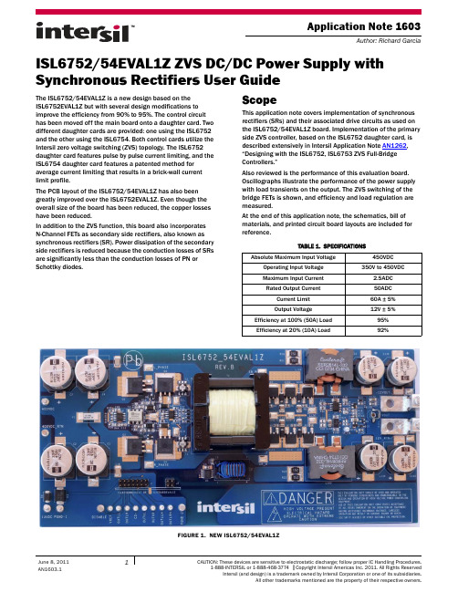
Application Note 1603Author: Richard GarciaISL6752/54EVAL1Z ZVS DC/DC Power Supply with Synchronous Rectifiers User GuideThe ISL6752/54EVAL1Z is a new design based on the ISL6752EVAL1Z but with several design modifications to improve the efficiency from 90% to 95%. The control circuit has been moved off the main board onto a daughter card. Two different daughter cards are provided: one using the ISL6752 and the other using the ISL6754. Both control cards utilize the Intersil zero voltage switching (ZVS) topology. The ISL6752 daughter card features pulse by pulse current limiting, and the ISL6754 daughter card features a patented method for average current limiting that results in a brick-wall current limit profile.The PCB layout of the ISL6752/54EVAL1Z has also been greatly improved over the ISL6752EVAL1Z. Even though the overall size of the board has been reduced, the copper losses have been reduced.In addition to the ZVS function, this board also incorporates N-Channel FETs as secondary side rectifiers, also known as synchronous rectifiers (SR). Power dissipation of the secondary side rectifiers is reduced because the conduction losses of SRs are significantly less than the conduction losses of PN or Schottky diodes.ScopeThis application note covers implementation of synchronous rectifiers (SRs) and their associated drive circuits as used on the ISL6752/54EVAL1Z board. Implementation of the primary side ZVS controller, based on the ISL6752 daughter card, is described extensively in Intersil Application Note AN1262, “Designing with the ISL6752, ISL6753 ZVS Full-Bridge Controllers.”Also reviewed is the performance of this evaluation board. Oscillographs illustrate the performance of the power supply with load transients on the output. The ZVS switching of the bridge FETs is shown, and efficiency and load regulation are measured.At the end of this application note, the schematics, bill of materials, and printed circuit board layouts are included for reference.TABLE 1.SPECIFICATIONSAbsolute Maximum Input Voltage450VDCOperating Input Voltage 350V to 450VDCMaximum Input Current 2.5ADC Rated Output Current50ADC Current Limit 60A ± 5%Output Voltage12V ± 5%Efficiency at 100% (50A) Load 95%Efficiency at 20% (10A) Load92%FIGURE 1.NEW ISL6752/54EVAL1ZBlock DiagramThe evaluation board is composed of several distinct circuit elements. The three main sections are the ZVS full bridge on the input, the current doubler rectifier on the output, and the controller daughter card. See “Schematics- Main Board,ISL6752/54EVAL1Z” on page23 and “Schematics - Daughter Card” on page25 for complete circuit details.Daughter CardsThe ISL6752 or ISL6754 control ICs are located on their respective daughter cards, as shown in Figures 3 and 4. Both daughter cards have the control ICs on the primary side and the voltage error amplifier on the secondary side. Creepage spacing between the primary and secondary is maintained on the cards. The ISL6752 and the ISL6754 control ICs are located on the primary side, eliminating the need for two AC line isolating gate drive transformers to drive the primary side bridge FETs. Instead, the low side FETs are driven directly by MOSFET drivers (on the main board), and the high side FETs are driven by a gate drive transformer that only requires operational insulation. Primary side control also simplifies design of the current sensing transformers because they also do not have to be AC line isolating.A line isolation rated opto-coupler (D5 on ISL6752DB or D2 on ISL6754DB) passes the analog error signal generated by the error amplifier, U1, from the secondary to the primary. Opto D3 passes a digital signal from primary to secondary to turn off the SRS for diode emulation. The only functional difference between the ISL6752 andISL6754 daughter cards is how current limit is implemented. The ISL6752 uses pulse-by-pulse current limit, and the ISL6754 uses average current limit.Special test points located on the daughter cards aid in probing nodes on the daughter cards for evaluation. Test points PGND and TP_PRI are located on the primary side, and SGND andTP_SEC are located on the secondary. With these test points, the user can employ the spring-like probe accessories included withFIGURE 2.ISL6752/54EVAL1Z BLOCK DIAGRAMFIGURE 3.ISL6752 DAUGHTER CARDmany scope probes. The scope signal pin is inserted in TP_PRI (or TP_SEC), and the short spring ground lead is inserted in PGND (or SGND).To probe any node on the daughter card, solder a 30ga insulated wire between the desired node and the via that is associated with the TP_PRI or TP_SEC test point. This method not only simplifies probing of any node, but also implements the preferredtechnique of measuring small signals in the presence of high amplitude switching magnetic fields.The ISL6752DBEVAL1Z and the ISL6754DBEVAL1Z daughter cards are also available as standalone evaluation kits.ZVS Full BridgeThe low side FETs, Q 3 and Q 4, are driven directly by the ISL89160 MOSFET driver, U1 (Figure 5). The two high-side FETs, Q 1 and Q 2, are indirectly driven by the ISL89160 driver, U2. A level translating gate drive transformer, T 3, with complementary output windings, directly drives the high-side bridge FETs with a symmetrical square wave. The design of T 3 is simplified because it only needs 400V operational insulation, and it is always driven with a square wave, thus eliminating the problems associated with non-symmetrical drive waveforms.Observe that the ISL89160 MOSFET drivers are located as close as possible to their respective bridge FETs to minimize thedetrimental effects of parasitic inductance on the outputs of the drivers. Although the input signal lead lengths between the drivers and the daughter card are relatively long (about 5cm), they are shielded on top and bottom by ground planes, to significantly reduce the noise injected on these lines. Thehysteresis of the ISL89160 inputs also lessens the possibility of noise corrupting the gate signals.High Voltage ProtectionBecause a failure of the bridge can cause catastrophic damage to the primary side control elements, a voltage crowbar, F1 and D 3, and a voltage blocking diode, D 4, are incorporated (Figure 6). D 3 clamps the bias voltage to a safe level. If 400V is applied to the V DD node, F1 opens shortly after D3 conducts current. D 4provides additional protection by blocking high voltage from being applied to the 13V lab supply. Note that a fully debugged power supply does not need these additional components. These parts are included on the evaluation board to minimize damage, should the user accidently introduce a fault while evaluating thecircuits. The designer may want to keep F1 in the final design, toprevent a loud bang if the bridge does fail.FIGURE 4.ISL6754 DAUGHTER CARDFIGURE 5.FULL BRIDGEFIGURE 6.PROTECTION CIRCUITSPrimary Side Current SensingThe primary side bridge has two current sensing transformers, T 2 and T 4, one on each leg on the drains of the low-side bridge FETs (Figure 7). Using two transformers allows each CT to reset during alternate half cycles. Alternate current sensing methods are reviewed in “Current Sensing” on page 8.Synchronous Rectifier Drive CircuitTwo banks of SRs are driven by the ISL89163 MOSFET driver, U4 (Figure 8). An RCD network on the inputs to this driver delay the turn-on of the SRs relative to the turn-off of the primary side bridge FETs.The ISL89367, U108, can optionally be used to drive the SRs instead of the ISL89163. Review “Schematics - Daughter Card” on page 25 to understand how to disconnect the ISL89163 and connect the ISL89367.The pulse transformer, T 6, crosses the isolation boundary to couple the control signals from the ISL6752, ISL6754 to the MOSFET drivers (Figure 9). Note that this transformer alsoprovides the secondary side bias voltage for the MOSFET drivers.Current Doubler OutputThe current doubler output is composed of two banks of SRs, Q 107... Q 109 and Q 111... Q 113; inductors L 102and L 103; and output filter capacitors, C 133... C 136 (Figure 10). The advantage of this topology is that the output current is shared by the two inductors, thus reducing conduction losses. Another advantage isthat the secondary winding of the power transformer does not require a center tap.FIGURE 7.PRIMARY SIDE CURRENT SENSINGFIGURE 8.SRs AND DRIVERSFIGURE 9.PULSE TRANSFORMER AND DRIVERBasic SR PrinciplesReplacing diodes with MOSFETs has two major advantages:•Dramatically reduces conduction losses•The applied duty cycle remains virtually constant from no load to full load. Disadvantages are:•Additional complexity and cost•Higher reverse recovery losses as compared to fast recovery diodes.•When paralleling units for redundancy, provisions must be made to prevent current circulation among the paralleled units.SR Drive Timing RequirementsTo emulate a diode, an SR must be driven ON when a diode would normally be conducting. But unlike a diode, if the SR is ON, the current through the SR can reverse if the voltage on the SR “cathode” becomes positive. The consequence is that if the SR is driven ON when the primary side is sourcing voltage to the secondary, the secondary side will be shorted by the SR. Figure 11 illustrates the timing required to drive the SRs. Notethat the rising edges of the two lower bridge FETs are delayed bythe ISL6752/54 relative to the PWM signal. Likewise, the risingedges of the SRs gate signals are delayed by the ISL89163relative to the falling edge of the PWM signal. These delays arenecessary to prevent the overlap of drive signals that wouldresult with high amplitude short circuit currents.When an SR is turned off while current is flowing from source todrain, the current diverts from the FET channel to the internalbody diode. Because the voltage drop across the body diode ishigher than the channel, it is desirable to minimize dissipation byminimizing the duration of the current flow through the bodydiode.FIGURE 10.CURRENT DOUBLER OUTPUTFIGURE 11.TIMING FOR SRs AND BRIDGE FETsSR Drive and BiasOUTLLN and OUTLRN in Figure 12 are control signals from the ISL6752/54 that are used to drive the SRs. Because theISL6752/54 is located on the primary side, a pulse transformer, T6, is used to cross the isolation boundary. The simplified schematic of Figure 12 illustrates the use of T6 to not only couple OUTLLN and OUTLRN to the secondary, but also to generate the bias for drivers on the secondary.When /OUTLLN or /OUTLRN (outputs of EL7212) transitions to a logic high, it is necessary to turn off the associated SR quickly. For example, when /OUTLRN (blue) transitions high, V1 is high, and C10 is quickly discharged by Q100. U4 then drives R-SR off. In a similar manner, when /OUTLLN is high, U4 drives L-SR off. When /OUTLLN or /OUTLRN transitions to a logic low, it is necessary to turn on the SRs after a time delay, to prevent the SRs from shorting the primary side bridge when it is sourcing current. For example, when /OUTLRN transitions to low, V1 is low and Q100 turns off, allowing C10 to be charged by R27. When the positive threshold of UR is exceeded, the output of U4 drives on R_SR. In a similar manner, the high to low transition of/OUTLLN results in the output of U4 driving on L_SR after a time delay.Note that the cathodes of D9 are connected together to peak charge C123. Because C123 is large in value, after the initial charging, the voltage does not change significantly from cycle to cycle. An important aspect of generating the bias for U4 in this manner is that the thresholds for the logic transitions on the inputs of U4 are proportional to VBIAS, and the voltage to charge C9 and C10 is also VBIAS. Consequently, the delays generated by the RC networks are independent of the absolute value of VBIAS. Current DoublerFigure 13 illustrates the current flow in the two inductors of the current doubler topology. Current flow in the circuit is correlated with the waveforms by color coding. The green waveform represents the sum of red and blue currents through R LOAD. For circuit clarity, paralleled SRs and output capacitors of theISL6752/54EVAL1Z board are not shown.When using diodes (instead of SRs), if the average load current is less than half of the ramp current in the output inductors, the current in the inductors becomes discontinuous, and the duty cycle of the PWM is shortened to maintain the desired output voltage. When using SRs, the inductor currents in L1 and L2 can become negative because current in SRs can flow bidirectionally; consequently, the duty cycle remains virtually unchanged. The benefit is that the load transient performance is the same for any load from zero up to current limit. Another advantage is that, for very light loads, the duty cycle is not reduced to very small duty cycles, pulse skipping does not occur, and the associated voltage jitter does not happen.An important design consideration for the current doubler topology is that the DC resistance of both halves must be equal. PCB layout must be as symmetrical as possible, and the DCRs of the inductors should be reasonably equal. If not, the current between the two sides does not split equally. Because perfect physical PCB symmetry is not always possible, current sharing between inductors must be confirmed.In Figure 14, inductor current waveforms are taken from the ISL6752/54EVAL1Z board. Current balance between the two inductors was achieved after one board revision. The inductor currents maintain the same waveform shape even at no load. Another design consideration when using SRs is how to connect the outputs of multiple power supplies in parallel for redundancy or increased power capacity. A consequence of negative current flow in an SR (when a diode would otherwise be reverse biased and off) is that power can be transferred from the secondary to the primary if one of the paralleled outputs has a higher voltage. The voltage loop of the units with lower set point voltages attempts to pull down the voltage by sinking current from the higher set point units. The primary side bridge capacitor is charged by the secondary side, eventually resulting in excessive voltage damage. This damage can be avoided by using OR-ing diodes (or FETs) on the paralleled outputs. Another solution is to turn off the SRs (diode emulation mode) when the current reverses in the SRs, but this eliminates some of the advantages of using SRs. Paralleling features are not implemented on the ISL6752/54EVAL1Z board.FIGURE 13.CURRENT FLOW IN TWO INDUCTORS OF CURRENT DOUBLER TOPOLOGYFIGURE 14.INDUCTOR CURRENT WAVEFORMS 50A LOAD30A LOAD NO LOADCurrent SensingCurrent flowing from the secondary to the primary can result in an unanticipated malfunction of the current sensing transformer circuit if reverse SR currents are not considered. Figure 15 shows a commonly used primary side current sensing circuit utilizing one current sensing transformer (CT).This circuit works well for peak current mode control if power is always flowing from primary to secondary, as is the case when diodes are used instead of SRs. Figure 16 illustrates the performance of the current sensing output when power always flows from primary to secondary.The voltage across R S is as expected. The vertical dashed lines show when the power cycle is terminated at the required peak of the current.Figure 17 illustrates what happens at no load to the sense voltage across R S.Notice that the negative components of the primary transformer current are rectified, resulting in two peaks of current across R S for each half cycle. Under steady state conditions, the rectified negative component may cause erratic performance because the cycle can terminate on the first peak (the inverted peak, as indicated by the vertical red line) instead of the required second peak. This condition can easily be corrected by having a small load across the output to ensure that the negative peak is always less than the positive.A minimum load, however, does not correct a more serious problem that occurs when there is a large load step from a heavy load to no load. When the load current is interrupted, the output capacitor charges higher than the regulated voltage. As the regulation loop is starting to respond by slewing to a minimum duty cycle, the excessive voltage on the output capacitor starts to discharge back to the primary. This results in a large negative current at the beginning of the duty cycle, which causes the duty cycle to be terminated very early. The imbalance of the applied volt-seconds to the power transformer may saturate the power transformer and damage the power bridge.Another scenario is that the current sensing transformer itself may saturate, which also damages the bridge. The control loop cannot maintain balanced alternate half cycles applied to the power transformer without valid current sense information. There are three solutions to this problem. Figure 18 illustrates the placements of two current sensing transformers, one on each drain leg of the bottom FETs.In this configuration, only positive current flowing into the drains of the bottom FETs are sensed across R S, solving the problem of rectified negative currents being impressed across R S. An advantage of using two CTs is that there is a full half cycle available to reset the cores of the CTs. This is the solution used in the ISL6752/54EVAL1Z board.FIGURE 15.PRIMARY SIDE CURRENT SENSING CIRCUIT UTILIZINGONE CTFIGURE 16.PERFORMANCE OF CURRENT SENSING OUTPUTFIGURE 17.NO LOAD SENSE VOLTAGE ACROSS R SFigure 19 shows a different current sensing implementation that also solves the problem shown in Figure 15. In this example, both drain currents of the bottom FETs are sensed by only one CT. There are some limitations that must be considered, however. The minimum time available to reset the core is the duration of the selected dead time between the two FETs on the same side of the bridge. To accommodate the resetting of the CT, this dead time can be made longer, but the consequences of reducing the maximum duty cycle available for output voltage regulation mustIf the dead time is kept short, then the peak voltage required for resetting the core is relatively large. For example, assume that the selected dead time is 2% of the duty cycle. The resultingworst-case reset voltage is shown approximately in Equation1:In Equation 1, V SMAX is 1V (the current limit voltage of theISL6752); this is the ideal reset voltage. In practice, however, the parasitic capacitance of the output windings suppresses the peak voltage, and consequently, the reset time increases. If a custom current sensing transformer is designed, the effects of the parasitic capacitance can be minimized by increasing the space between turns. If a standard, off-the-shelf transformer is used, however, the output capacitance may be too large to allow long duty cycles. In this case, the two-transformer solution may be necessary.Notice in Figure 19 that the 400V RTN is slightly more negative than signal ground. This configuration is recommended for applications that directly drive the bottom FETs with MOSFET drivers. If the 400V RTN and the MOSFET drivers are grounded, regenerative feedback will be present on the output of the MOSFET drivers because of the CT windings in the gate drive loop.A variation on the current sense circuit in Figure 19 is to place the current sensing transformer in the common drain lead of the two high-side FETs, as shown in Figure 20.The circuits shown in Figures 19 and 20 give exactly the same performance, but the problem associated with the gate drives (as explained in Figure 19) is avoided. The disadvantage of placing the CT at this location is that the CT must be designed with400VDC operational insulation.ConclusionThis application note reviews the use of MOSFETs as synchronous rectifiers to replace conventional diodes. The advantages of improved power efficiency and load transient are reviewed along with implementation problems that must be solved.The use of daughter cards for the ISL6752 and ISL6754 control ICs also allows comparison of cycle-by-cycle peak current limiting and average current limiting.TRANSFORMERSFIGURE 19.CURRENT SENSING TRANSFORMER IN THE COMMON SOURCE LEAD0.980.02⁄()V SMAX49V=•(EQ. 1)FIGURE 20.DRAIN LEADReferences[1]Fred Greenfeld, Intersil Application Note AN1246,“Techniques to Improve ZVS Full-bridge Performance”[2]Fred Greenfeld, Intersil Application Note AN1262, “Designingwith the ISL6752, ISL6753 ZVS Full-bridge Controllers”[3]Richard Garcia, Intersil Application Note AN1619, “Designingwith ISL6752DBEVAL1Z and ISL6754DBEVAL1Z ControlCards”Evaluation Board Set-upThe following sections cover the set-up of theISL6752/54EVAL1Z evaluation board. Also included are waveforms, performance parameters, PCB layout, and schematics.Setting UpLab Equipment Required•DC bias power supply, 12.6VDC @ 200mA minimum •Adjustable 0VDC-400VDC regulated lab power supply, 2.5ADC minimum with current limit•Fan to cool heatsinks•Oscilloscope, digital preferred, with 4 channels, 20MHz minimum bandwidth•Adjustable DC load (electronic or resistor), 70A @ 12V,100A @ 0V min, >850W•DC Multimeter•Infra-red temperature probe (optional but highly recommended)Turn-On Procedure1.Solder a wire between DISABLE and PGND-1 lugs located onthe lower left side of the main board. Optionally connect a switch between these two lugs.2.Install either of the daughter control cards onto the mainboard.3.Connect the DC load to the outputs of the evaluation board.Adjust the load to zero current.4.With both supplies turned off, connect the DC bias supply tothe +13V terminal and PGND.5.Connect the 400V supply to +400V and 400V RTN.6.Turn on the DC bias supply and adjust the current limit to200mA. Adjust the voltage to +12.6 VDC. The lab supplycurrent should be approximately 150mA.7.Turn on the 400V supply and adjust the current limit to 2.5A.Adjust the voltage to 400VDC. Do not exceed 450VDC. The current should be approximately 45mA.8.Turn on the fan and direct the air flow through the heatsinksmounted on the bottom of the board.ing the test points that are adjacent to the output powerlugs, measure the output voltage of 12V ±0.5VDC.The output load and input voltage can now be safely adjusted. Because there is no thermal shut-down circuit, it is important to maintain adequate airflow over the heatsinks, especially when applying large loads. It is recommended to measure the temperature of the power FETs (primary bridge and secondary SRs) to ensure that their temperatures do not exceed +85°C. It is usually necessary to have only a moderate airflow over the heatsinks, even under worst-case loads.Danger•This evaluation unit should be used and operated only by persons experienced and knowledgeable in the design and operation of high voltage power conversion equipment. •Use of this evaluation unit constitutes acceptance of all risk inherent in the operation of equipment having accessible hazardous voltage. Careless operation may result in serious injury or death.•Use safety glasses or other suitable eye protection.•A line isolated 400VDC supply is required. CautionA voltage clamp, D3, is used to protect the primary side control circuit from catastrophic damage should the high voltage bridge fail. In order to prevent this clamp from conducting, do not adjust the bias supply above 13.5VDC.WaveformsZVSIn Figure 21, the drain-source voltage of the low-side FETs relative to the gate voltage is displayed to highlight the ZVS performance of the bridge. The load is at the rated 50A. Notice that full ZVS is not achieved because the minimum resonance voltage is about 25VDC. Also, the gate drive is turning on late (about 25ns), allowing the resonant voltage to start rising. Eventhough the optimum zero voltage switching is not achieved, 98% of the switching losses are still recovered [(4002-502)/4002=98%]. This improvement over the ISL6752EVALZ was achieved by increasing the leakage inductance of thetransformer and by using bridge FETs with less body capacitance.In Figure 22, resonant switching with 50% load still saves 84% of the switching losses. Other techniques can be used to improve ZVS performance. For more information, see Application NoteAN1246, “Techniques to Improve ZVS Ful-bridge Performance”.ZVS WaveformsFIGURE 21.RESONANT SWITCHING WITH 100% (50A) LOADFIGURE 22.RESONANT SWITCHING WITH 50% (25A) LOADLoad Transients WaveformsFIGURE 23.STEP LOAD: 0A TO 12.5A (12.5A DELTA)FIGURE 24.STEP LOAD: 25A TO 37.5A (12.5A DELTA)FIGURE 25.STEP LOAD: 37.5A TO 50AFIGURE 26.STEP LOAD: 0A TO 25AFIGURE 27.STEP LOAD: 0A TO 50AFIGURE 28.SHORT CIRCUIT RELEASE WITH ISL6754V OUT recovers after a short circuit is removed when using the ISL6754DBEVAL controller.After the short is removed, V OUT increases linearly because the output capacitance is being charged with a constant current (~55A).NOTE:Output Ripple and Noise WaveformsFIGURE 29.OUTPUT RIPPLE, 50A LOAD, 40MHz BANDWIDTHFIGURE 30.OUTPUT RIPPLE, 50A LOAD, 145MHz BANDWIDTHTransformer Current, Primary Winding WaveformsFIGURE 31.PRIMARY TRANSFORMER CURRENT vs OUTPUT LOAD TRANSIENT (25A TO 50A)FIGURE 32.PRIMARY TRANSFORMER CURRENT vs OUTPUT LOAD TRANSIENT (50A TO 25A)Performance CurvesFIGURE 33.POWER EFFICIENCY vs LOAD (ISL6752 OR ISL6754)FIGURE 34.LOAD REGULATION FIGURE 35.PULSE BY PULSE vs AVERAGE CURRENT LIMIT21015202570758085909295100OUTPUT CURRENT (A)E F F I C I E N C Y (%)6560555030354045505592% EFFICIENCY WITH 20% LOAD12.0011.9511.9011.8511.80ISL6754ISL6752102030405060I OUT (A)V O U T (V )01020304050607080I OUT (A)V O U T (V )121086420ISL6754ISL6752Application Note 1603Bill of MaterialsPART NUMBERQTY UNITS REFERENCE DESIGNATORDESCRIPTION MANUFACTURER MANUFACTURER PART ISL6752/54EVAL1ZREVBPCB1eaPWB-PCB,ISL6752_54EVAL1Z, REV B, ROHSIMAGINEERING INCISL6752/54EVAL1ZREVBPC BC3216X7R1C475K-T 2eaC11, C17CAPACITOR, SMD, 1206, 4.7µF, 16V, 10%, X7R, ROHSTDK C3216X7R1C475KC4532X7R2J104K-T 2ea C5, C18CAP, SMD, 1812, 0.1µF, 630V, 10%, X7R, ROHSTDKC4532X7R2J104K GA355QR7GF332KW01L-T 2ea C20, C121CAP, SMD, 2220, 3300pF, 250V, 10%, X7R, ROHSMURATA GA355QR7GF332KW01L H1046-00102-100V10-T 2ea C14, C15CAP, SMD, 0805, 1000pF, 100V, 10%, X7R, ROHSVENKEL C0805X7R101-102KNE H1046-00102-50V5-T 2ea C9, C10CAP, SMD, 0805, 1000pF, 50V, 5%, NP0, ROHS PANASONIC ECU-V1H102JCX H1046-00105-25V10-T 5ea C6, C12, C13, C16, C22CAP, SMD, 0805, 1.0µF, 25V, 10%, X5R, ROHS AVX 08053C105KAT2A H1065-00106-25V10-T 1ea C123, C132CAP, SMD, 1206, 10µF, 25V, 10%, X5R, ROHS VENKEL C1206X5R250-106KNE H1082-00475-50V10-T 4ea C7, C8, C127, C129CAP, SMD, 1210, 4.7µF, 50V, 10%, X7R, ROHS MURATA GRM32ER71H475KA88L SER2814L-332KL2eaL102, L103COIL-PWR INDUCTOR, SMD, 3.3µH, 10%, 48A, 1.2m Ω, ROHS COILCRAFTSER2814L-332KLUUG1C222MNL1ZD 4ea C133-C136CAP, SMD, 16X16.5, 2200µF, 16V, 20%, AL.EL., ROHS NICHICON UUG1C222MNL1ZDUUG2W330MNL1MS 4ea C1-C4CAP, SMD, 18X21.5, 33µF, 450V, 20%, ALUM.ELEC, ROHS NICHICON UUG2W330MNL1MS131-4353-001ea VOUT CONN-SCOPE PROBE TEST PT, COMPACT, PCBMNT, ROHSTEKTRONIX 131-4353-001514-26eaa) 13VDC, 400VDC, PGND-1, PGND-2, DISABLE CONN-TURRET, TERMINAL POST, TH, ROHSKEYSTONE 1514-21514-20ea b) 400VDC_RTNCONN-TURRET, TERMINAL POST, TH, ROHSKEYSTONE 1514-250029ea a) CS+, VREF, OUTLL, OUTLR, OUTUL, OUTUR CONN-MINI TEST POINT, VERTICAL, WHITE, ROHS KEYSTONE500250020ea b) SR_EN, OUTLLN, OUTLRNCONN-MINI TEST POINT, VERTICAL, WHITE, ROHSKEYSTONE 50025016-T13eaa) GLL, GLR, LLN, LRN, SR_A, SR_B, PGND-3, 2, +12VOUT, 12V RTN CONN-COMPACT TEST POINT, SMD, ROHS KEYSTONE50165016-T 0ea b) SGND-1, SGND-CONN-COMPACT TEST POINT, SMD, ROHSKEYSTONE 50165016-Teac) L_PHASE, R_PHASE CONN-COMPACT TESTPOINT, SMD, ROHSKEYSTONE5016。
威森特常规产品报价
对每个常规 网络摄型号分850S 特价960P 130万860S 爆款960P 130万960S-AV 音频版 960P 130万华为海思1082S-AV 音频版1080P 200万型号分2501S (H.265)06SE 960P 9003(捷安锐视)1080P1300S 960P1185S 星光全彩1080P日夜全彩 白光摄像机1600S1080P 9200S 1080P型号分型号分6130S-AV 音频版960P 6200S-AV 音频版1080P 3MP型号分 1086S 推荐1080P 200万型号分5130S960P 861S960P 130万 862S 爆款960P 130万 1083S1080P 200万2506S (H.265)智能球形变倍一体机特殊场合 网络红激光 夜视王7621S 1080P 型号分型号分7613S960P 7620S1080P Q1960P 1305倍Q2 1080P 2 5倍Q3 1080P 2 25倍3MP型号分特点:室内室外防雨 4.5寸迷你球机 6颗阵列红外灯 5倍支持360度旋转 支持预置位 支持手机远程控制、手机录像。
可无线连4.5寸迷你球道路车牌摄像机防爆摄像机防爆摄像机电梯专用摄像机银行专用摄像机2081S 全彩低照度1080P 2061S 全彩低照度1080P 型号分2080S1080P 6203S 音频版3MP 型号分2060S960P 型号分 6201S 音频版1080P 6202S 音频版1080P 6003S960P 6013S 1080P6033S1080P L6001080P L7001085P型号分L500960P9615AH AHD同轴960P 9610AH AHD同轴9196AH AHD同轴960P960P9612AH AHD同轴960P2000HD 模拟005HK 模拟81000TVL 605HD 模拟1000TVL型号分型号分型号分型号分模拟摄像机 AHD同型号分9660AH AHD同轴960P 7118HD 模拟812路 NVR 型号Smart-916S 16路画面显示 支持1块硬模式1:接入16路108支持自组网一键添加 ,支持音频输出 可接音响耳机 即插即用,型号Smart-912S 12路画面显示,支持1块硬模式1:接入12路96模式2:接入9路108支持音频输出 可接音响耳机 即插即用,NVR网络录像型号Smart-904S 6路画面显示,支持1块硬支持 接入6路1080支持自组网一键添加 ,支持音频输出 可接音响耳机 即插即用,型号Smart-906S 6路画面显示,支持1块硬6路 NVR 4路 NVR 支持 接入6路108025路 NVR 4路 混合录像机16路 NVR 36路 NVR 4盘位即插即用,一键远程4合一 混合硬盘型号:6804S 4路画面显示,支持1块硬盘同时支持模拟摄像机、AH支持自组网一键添加 ,即插即用,一键支持自组网一键添加 ,支持音频输出 可接音响耳机 即插即用,型号Smart-936S 36路画面显示,支持4块硬模式1:接入36路96模式2:接入35路108型号:6808S 8路画面显示,支持1块硬盘同时支持模拟摄像机、AH即插即用型号Smart-925S 25路画面显示,支持2块硬模式1:接入25路108H.265 NVR录像机 4路 H.265 NVR 8路 混合录像机16路 混合录像机32路 混合录像机支持V390全景摄像机 多种模式显示 支持自型号:9804S 4路画面显示,支持1块硬盘存储减半 最高支持支持V390全景摄像机 多种模式显示 支持自即插即用,一键型号:9808S 8路画面显示,支持1块硬盘存储减半 最高支持支持自组网一键添加 ,即插即用,一键型号:6632S 32路画面显示,支持4块硬盘同时支持模拟摄像机、AH支持自组网一键添加 ,即插即用,一键即插即用,一键型号:6616S 16路画面显示,支持2块硬盘同时支持模拟摄像机、AHPOE 网络监一根网络线 同时传输电源与信号8路 H.265 NVR 32路 H.265 NVR 16路 H.265 NVR 一根网络线 同时传输电源无需交换机、无需电源线型960P 130万华为海思方案一根网络线 同时传输电源型号:9832S 32路画面显示,支持4块硬盘存储减半 最高支持支持V390全景摄像机 多种模式显示 支持自即插即用,一键型960P 130万华为海思方案即插即用,一键型号:9816S 8路画面显示,支持1块硬盘存储减半 最高支持支持V390全景摄像机 多种模式显示 支持自即插即用,一键全景 网络监一台顶多台 全方位无死角监控 同步录音录4路 POE NVR 8路 POE NVR 型号:3 300万像素支持语音对讲 远程监最大支持128G TF卡共计9个网口 8个网口支持2块硬盘,型号:1200万像素支持语音对讲 远程监最大支持128G TF卡内置拾音器,V6方型4路画面显示 接入最大4共计5个网口 4个网口无需交换机 支型8路画面显示接入 最大8无需交换机、无需电源线免布线 电力网络一根电力线 同时传输多个摄像机 最远60 农行卡号:622 849 06300 1210 9510 户名:孙恒 邮政新卡号: 622 188 12100 2364 9705 户名:孙恒资中行:6216 615 00000 2408 071 户名:孙恒资工商:6222 08040 20014 07068 户名:孙恒资 开户行:中华 建行:4367 4201 3039 8652 954 户名:孙恒资支付宝:136******** 孙国强 以上报价不含税票及运费 (公司可开增全景专用 8路NVR 全景专用 4路NVR 最高可接入4路5M支持HDMI输出 即插即用,一键远型号 9808 8路画面显示,支持1块硬盘支持2分割画面、4分最高可接入8路5M支持HDMI输出 即插即用,一键远内置拾音器,V6方型号 9804 4路画面显示,支持1块硬盘支持2分割画面、电力网络传可实现电力猫功省去交换机、电源线、网支持任何品牌网络电力需配合 电力网络传省去交换机、电源线、网支持任何品牌网络10台起 价格69元76元100元12610台起 价格网络摄像机V6方案 H.264压缩格式全铝合金结构 75口径2颗晶元点阵红外灯最远夜视距离50米以上性能130万像素 华为海思200万像素 华为海思分辨率分辨率性能 130万像素 国科芯片130万像素 V6AK芯片全铝合金结构 100口径机机195元机机130元220元VIP价格60元75元力猫功能 同电表内 多个使用线、网线、监控电源、防水盒一半人工费牌网络NVR录像机、网络IPC摄像机电力网络接收器网络传输器 (发射器 )。
松下 数码相机 DC-G100 使用说明书

池或重新连接交流电源适配器,再将本机打开。
请勿在无线电发射器或高压线附近使用本机。 • 如果您在无线电发射器或高压线附近拍摄,拍摄的图像和/
或声音可能会受到不良影响。
DVQX2059 (SCH)
7
安全注意事项
• 要清洁您的相机,请卸下电池或卡,或从插座拔下电源插 头,然后用软干布擦拭。
保持本机远离电磁设备(例如微波炉、电视机、游戏机等)。 • 如果您在电视机上面或附近使用本机,本机上的图像和/或
声音可能被电磁波辐射干扰。 • 请勿在移动电话附近使用本机,否则噪声可能对图像和/或
声音产生不良影响。 • 扬声器或大型电机产生的强大磁场可能造成记录的数据损坏
或图像失真。 • 电磁波辐射可能对本机造成不良影响,干扰图像和/或声音。 • 如果本机受电磁设备的不良影响而不能正常工作,请关闭本
使用注意事项
• 除了随机附送的以外,请勿使用任何其他USB连接电缆。 • 除了随机附送的或正品Panasonic手柄(DMW-SHGR1 :另售)
以外,请勿使用任何其他手柄。 • 使用带有HDMI标志的“高速HDMImicro电缆”。
不符合HDMI标准的电缆不能工作。
“高速HDMImicro电缆”(D型-A型插头,最长2 m) • 请勿使用3 m或以上长度的立体声麦克风电线。
10 DVQX2059 (SCH)
目录6. 驱动/图像稳定器55选择驱动模式 ................................ 55 图像稳定器 .................................. 56
7. 亮度(曝光)/着色/图像效果
57
[测光模式].................................. 57 曝光补偿 .................................... 58 ISO感光度 ................................... 59 白平衡(WB)................................. 61
Riegl VZ-6000中文介绍

利用全站仪拼接
精确扫描已知的远处物体(反射片) RiSCAN PRO 后视点处理功能
设置已知的站点(内置激光铅锤) 内置倾斜补偿传感器
RIEGL VZ®-6000 扫描仪的操作原理和连接
WLAN 天线 搬运手柄
激光开启指示器
高分辨率 7〞彩色触摸屏
450
激光开启指示器
电 源 接 口 , LAN 数 据 接 口 10/100/1000MBit/s,电源开关
dry snow
dry snow
90
Target Reflectivity [%]
Target Reflectivity [%]
200 kHz PRR
6500
6500
300 kHz PRR
6000
6000
5500
5500
5000
5000
4500
4500
4000 3750 3500
MTA 6
4000
3500
5)
接收最大回波次数
6) 8)
3 800 m 4) 2 100 m 4)
3 300 m 4) 1 800 m 4)
精度 重复测量精度 7) 8) 最近测量距离 激光波长 激光发散度 9) (Gaussian Beam Definition) 激光光斑
测量原理:
基于时间-飞行差脉冲测量,全回波,实时波形分析
操作模式:
激光最大发射频率 2)
有效测量频率 3) 最大测距 物体反射率 ≥ 90 % 物体反射率 ≥ 20 %
2)
全波形输出(可选的) 单一脉冲范围
50 kHz 100 kHz 200 kHz 300 kHz 37 000 meas./sec 74 000 meas./sec 147 000 meas./sec 222 000 meas./sec 6 000 m 4) 3 600 m 4 800 m 4) 2 800 m 4) 无穷次
价格对比
汉柏 型号 List 76500 18500 175000 81000 53000 14850 代理商折扣 用户折扣
神州数码(代理商折扣1.2-1.5,用户折扣1.8-2. 型号 DCRS-5960-28T DCRS-5750-28T DCS-3950-28C DCFW-1800E-N5002 DCWL-ZD-1006 带25AP许可增加 DCWL-ZF-7942AP-L List 80000 35000 16600 220000 43000 60000 12500
锐捷 List 79810 18000 340000 13300 20000
锐捷 代理商折扣 用户折扣
思科 型号 List 代理商折扣 用户折扣 WS-C3750V2-23TS-S $3,995 1.8 7200 WS-C2960S-24TS-L 33% 38% ASA5510-K8 $7,340 1.5 11000 HW-3000-MNT-19 LIC-PEFNG-32 AP-90-MNT $4,493 1.45 6500 型号
三层交换机 PT-3750E-28T 二层交换机 安全网关 PT-2960-28T
PA-5500-U20B PW-MC1500 无线控制器 带25AP许可增加 无线AP PWA-1010i
扣1.2-1.5,用户折扣1.8-2.5) 代理商折扣 用户折扣
H3C(比神码贵5%-10%)
1.2-1.5
型号 List 代理商折扣 用户折扣 LS-S5600-26C 80000 LS-5500-28C-EI 54000 H3C S3600-28TP-SI 18000 LS-3100-26TP-EI-H3-A 26500 1.8-2.5 2.2 2.4 H3C SecPath F1000-E-SI523000 EWP-WX5004-H3(缺 245500 省规格可管理64个AP) EWP-WA1208E-GP 12500
Z2系列直流电机
Z2系列直流电机Z2系列直流电动机是我国60年代研制开发的中小型直流电动机,具有性能可靠、价格便宜的优点,目前仍然广泛用于印染机械、包装机械、塑料机械等行业。
一、技术参数Z2系列电动机(220伏,1500转/分)电动机还可以制成额定电压为110V、160V、340V、440V、460V,额定转速为3000转、1000转、750转、600转等派生系列电动机,详细资料与本公司联系。
Z2系列发电机(115伏,1450转/分)发电机还可以制成115V 2850转/分、230V 2850转/分、230V 1450转/分等电压及转速等级的电机武汉索特南洋电机有限公司拥有雄厚的技术力量,先进的生产工艺装备,质量检验体系和管理水平。
并多次获得用户单位和地区的好评,获得“信用AAA”和“守合同重信用单位”等信誉称号。
武汉索特南洋电机有限公司的理念:提供专用的产品,提供专业的服务,打造专注的团队,成就专享的人生。
我们将恪守满足需要创品牌,诚信经营,求发展的方针,竭诚为客户提供满意的产品和专业的服务。
根据用户需要,可配置多速、高效、直流等多种电机,并可装置制动器或单向停止器。
我武汉索特南洋电机有限公司是专业电机制造商,主要生产销售:水冷电机、细纱机电机、炉用电机、变频电机、防爆电机、辊道电机、直流电机、起重电机、特种电机,以及各种非标产品设计与生产。
该系列产品适用于高温环境、变频调速系统。
其特点是调速范围广、运行稳定、可靠性高、运行效率高、外观设计美观。
产品具有独特的冷却系统可保证电动机在外界环境温度很高的情况下长期运行时的稳定工作,能耐高温高湿、防腐等特点。
广泛应用于军工、航天、污水处理、冶金、轻工、化工、钢铁、水泥、印刷、制糖、食品、橡胶、医药、建筑、起重、运输、木工机械、仪器仪表等行业。
武汉索特南洋电机有限公司力求以最优的质量,最快的速度,最有效的方式竭诚为用户服务,诚挚地与各界朋友合作,共谋发展。
武汉南洋电机联系方式电话:400-0988-308(全国免费)************传真:************e-mail:*****************地址:武汉市汉口沿江大道160号武昌火车站乘车线路:乘坐402路公交至沿江大道兰陵路站下,步行至兰陵路口往里100米即到汉口火车站乘车线路:乘坐603、38路公交至沿江大道兰陵路站下,步行至兰陵路口往里100米即到武汉市内公交路线:526、588、721、523、601、502、603、801、802等公交至沿江大道兰陵路站下,步行至兰陵路口往里100米即到以上资料来源/部分电机参数商品描述:YTAE变频系列电磁制动三相异步电动机是按JB/T6456-92标准制造的带交流圆盘式电磁制动器的三相异步电动机。
Z系列二极管参数
Z系列⼆极管参数Z系列⼆极管参数型号PDF资料⼚商特性⽤途极限⼯作电压Vrwm(V)极限⼯作电流Im(A)耗散功率Pw(w)最⾼⼯作频率fm(Hz)代换型号ZMM55-C3V6 BILIN 3.6V稳压⼆极管 3.6 0.5 ZMM55-C3V9 BILIN 3.9V稳压⼆极管 3.9 0.5 ZMM55-C43 BILIN 43V稳压⼆极管43 0.5 ZMM55-C47 BILIN 47V稳压⼆极管47 0.5 ZMM55-C4V3 BILIN 4.3V稳压⼆极管 4.3 0.5 ZMM55-C4V7 BILIN 4.7V稳压⼆极管 4.7 0.5 ZMM55-C5V1 BILIN 5.1V稳压⼆极管 5.1 0.5 ZMM55-C5V6 BILIN 5.6V稳压⼆极管 5.6 0.5 ZMM55-C6V2 BILIN 6.2V稳压⼆极管 6.2 0.5 ZMM55-C6V8 BILIN 6.8V稳压⼆极管 6.8 0.5 ZMM55-C7V5 BILIN 7.5V稳压⼆极管7.5 0.5 ZMM55-C8V2 BILIN 8.2V稳压⼆极管8.2 0.5 ZMM55-C9V1 BILIN 9.1V稳压⼆极管9.1 0.5 ZP10整流⼆极管3000 10ZP100整流⼆极管3000 100ZP100/100整流⼆极管100 100ZP100/1000整流⼆极管1000 100ZP100/1200整流⼆极管1200 100ZP100/1400整流⼆极管1400 100ZP100/1600整流⼆极管1600 100ZP100/200整流⼆极管200 100ZP100/300整流⼆极管300 100ZP100/400整流⼆极管400 100ZP100/500整流⼆极管500 100ZP100/600整流⼆极管600 100ZP100/700整流⼆极管700 100ZP100/800整流⼆极管800 100ZP100/900整流⼆极管900 100ZP1000整流⼆极管3000 1000ZP1000/100整流⼆极管100 1000型号PDF资料⼚商特性⽤途极限⼯作电压Vrwm(V)极限⼯作电流Im(A)耗散功率Pw(w)最⾼⼯作频率fm(Hz)代换型号ZP1000/1000整流⼆极管1000 1000 ZP1000/1200整流⼆极管1200 1000 ZP1000/1400整流⼆极管1400 1000 ZP1000/1600整流⼆极管1600 1000 ZP1000/1800整流⼆极管1800 1000 ZP1000/200整流⼆极管200 1000 ZP1000/2000整流⼆极管2000 1000 ZP1000/300整流⼆极管300 1000 ZP1000/400整流⼆极管400 1000 ZP1000/500整流⼆极管500 1000 ZP1000/600整流⼆极管600 1000 ZP1000/700整流⼆极管700 1000 ZP1000/800整流⼆极管800 1000ZP1000/900整流⼆极管900 1000 ZP10A整流⼆极管25 10 ZP10B整流⼆极管50 10 ZP10C整流⼆极管100 10 ZP10D整流⼆极管200 10 ZP10E整流⼆极管300 10 ZP10F整流⼆极管400 10 ZP10G整流⼆极管500 10 ZP10H整流⼆极管600 10 ZP10J整流⼆极管700 10 ZP10K整流⼆极管800 10 ZP10L整流⼆极管900 10 ZP10N整流⼆极管1200 10 ZP10P整流⼆极管1400 10 ZP10Q整流⼆极管1600 10 ZP10R整流⼆极管1800 10 ZP10S整流⼆极管2000 10型号PDF资料⼚商特性⽤途极限⼯作电压Vrwm(V)极限⼯作电流Im(A)耗散功率Pw(w)最⾼⼯作频率fm(Hz)代换型号ZP1500整流⼆极管3000 1500ZP20整流⼆极管3000 20ZP200整流⼆极管3000 200 R50210010RSWA,10SM200 ZP200/100整流⼆极管100 200ZP200/1000整流⼆极管1000 200ZP200/1200整流⼆极管1200 200ZP200/1400整流⼆极管1400 200ZP200/1600整流⼆极管1600 200ZP200/1800整流⼆极管1800 200ZP200/200整流⼆极管200 200ZP200/300整流⼆极管300 200ZP200/400整流⼆极管400 200ZP200/500整流⼆极管500 200ZP200/600整流⼆极管600 200ZP200/700整流⼆极管700 200ZP200/800整流⼆极管800 200ZP200/900整流⼆极管900 200ZP2000整流⼆极管3000 2000ZP20A整流⼆极管25 20ZP20B整流⼆极管50 20ZP20C整流⼆极管100 20ZP20D整流⼆极管200 20ZP20E整流⼆极管300 20ZP20F整流⼆极管400 20ZP20G整流⼆极管500 20ZP20H整流⼆极管600 20ZP20J整流⼆极管700 20ZP20K整流⼆极管800 20ZP20L整流⼆极管900 20ZP20M整流⼆极管1000 20型号PDF资料⼚商特性⽤途极限⼯作电压Vrwm(V)极限⼯作电流Im(A)耗散功率Pw(w)最⾼⼯作频率fm(Hz)代换型号ZP20P整流⼆极管1400 20 ZP20Q整流⼆极管1600 20 ZP20R整流⼆极管1800 20 ZP20S整流⼆极管2000 20 ZP30整流⼆极管3000 30 ZP300整流⼆极管3000 300 ZP300/100整流⼆极管100 300 ZP300/1000整流⼆极管1000 300 ZP300/1200整流⼆极管1200 300 ZP300/1400整流⼆极管1400 300 ZP300/1600整流⼆极管1600 300 ZP300/1800整流⼆极管1800 300 ZP300/200整流⼆极管200 300 ZP300/2000整流⼆极管2000 300 ZP300/300整流⼆极管300 300 ZP300/400整流⼆极管400 300 ZP300/500整流⼆极管500 300 ZP300/600整流⼆极管600 300 ZP300/700整流⼆极管700 300 ZP300/800整流⼆极管800 300 ZP300/900整流⼆极管900 300 ZP400整流⼆极管3000 400 ZP5整流⼆极管3000 5 ZP50整流⼆极管3000 50 ZP500整流⼆极管3000 500 ZP500/100整流⼆极管100 500 ZP500/1000整流⼆极管1000 500 ZP500/1200整流⼆极管1200 500 ZP500/1400整流⼆极管1400 500型号PDF资料⼚商特性⽤途极限⼯作电压Vrwm(V)极限⼯作电流Im(A)耗散功率Pw(w)最⾼⼯作频率fm(Hz)代换型号ZP500/1600整流⼆极管1600 500 ZP500/1800整流⼆极管1800 500 ZP500/200整流⼆极管200 500 ZP500/2000整流⼆极管2000 500 ZP500/300整流⼆极管300 500 ZP500/400整流⼆极管400 500 ZP500/500整流⼆极管500 500 ZP500/600整流⼆极管600 500 ZP500/700整流⼆极管700 500 ZP500/800整流⼆极管800 500 ZP500/900整流⼆极管900 500 ZP50A整流⼆极管25 50 ZP50B整流⼆极管50 50 ZP50C整流⼆极管100 50 ZP50D整流⼆极管200 50 ZP50E整流⼆极管300 50 ZP50F整流⼆极管400 50 ZP50G整流⼆极管500 50 ZP50H整流⼆极管600 50ZP50N整流⼆极管1200 50 ZP50P整流⼆极管1400 50 ZP50Q整流⼆极管1600 50 ZP50R整流⼆极管1800 50 ZP50S整流⼆极管2000 50 ZP55A整流⼆极管25 1 ZP55B整流⼆极管50 1型号PDF资料⼚商特性⽤途极限⼯作电压Vrwm(V)极限⼯作电流Im(A)耗散功率Pw(w)最⾼⼯作频率fm(Hz)代换型号ZP55C整流⼆极管100 1 ZP55D整流⼆极管200 1 ZP55E整流⼆极管300 1 ZP55F整流⼆极管400 1 ZP55G整流⼆极管500 1 ZP55H整流⼆极管600 1 ZP55J整流⼆极管700 1 ZP55K整流⼆极管800 1 ZP55L整流⼆极管900 1 ZP55M整流⼆极管1000 1 ZP55N整流⼆极管1200 1 ZP57A整流⼆极管25 25 ZP57B整流⼆极管50 25 ZP57C整流⼆极管100 25 ZP57D整流⼆极管200 25 ZP57E整流⼆极管300 25 ZP57F整流⼆极管400 25 ZP57G整流⼆极管500 25 ZP57H整流⼆极管600 25 ZP57K整流⼆极管800 25 ZP57L整流⼆极管900 25 ZP57M整流⼆极管1000 25 ZP59A整流⼆极管25 20 ZP59B整流⼆极管50 20 ZP59C整流⼆极管100 20 ZP59D整流⼆极管200 20 ZP59E整流⼆极管300 20 ZP59F整流⼆极管400 20 ZP59G整流⼆极管500 20 ZP59H整流⼆极管600 20型号PDF资料⼚商特性⽤途极限⼯作电压Vrwm(V)极限⼯作电流Im(A)耗散功率Pw(w)最⾼⼯作频率fm(Hz)代换型号ZP59J整流⼆极管700 20 ZP59K整流⼆极管800 20 ZP59L整流⼆极管900 20 ZP59M整流⼆极管1000 20 ZP59S整流⼆极管2000 20 ZP5A整流⼆极管25 5ZP5G整流⼆极管500 5 ZP5H整流⼆极管600 5 ZP5J整流⼆极管700 5 ZP5K整流⼆极管800 5 ZP5L整流⼆极管900 5 ZP5M整流⼆极管1000 5 ZP5N整流⼆极管1200 5 ZP5P整流⼆极管1400 5 ZP5Q整流⼆极管1600 5 ZP5R整流⼆极管1800 5 ZP5S整流⼆极管2000 5 ZP600整流⼆极管3000 600 ZP800整流⼆极管3000 800 ZP800/100整流⼆极管100 800 ZP800/1000整流⼆极管1000 800 ZP800/1200整流⼆极管1200 800 ZP800/1400整流⼆极管1400 800 ZP800/1600整流⼆极管1600 800 ZP800/1800整流⼆极管1800 800 ZP800/200整流⼆极管200 800型号PDF资料⼚商特性⽤途极限⼯作电压Vrwm(V)极限⼯作电流Im(A)耗散功率Pw(w)最⾼⼯作频率fm(Hz)代换型号ZP800/2000整流⼆极管2000 800 ZP800/300整流⼆极管300 800 ZP800/400整流⼆极管400 800 ZP800/500整流⼆极管500 800 ZP800/600整流⼆极管600 800 ZP800/700整流⼆极管700 800 ZP800/800整流⼆极管800 800 ZP800/900整流⼆极管900 800。
,ISL28136FHZ-T7A,ISL28136FBZ-T7,ISL28136FHZ-T7,ISL28136FBZ,ISL28136EVAL1Z, 规格书,Datasheet 资料
•Compatible with most vacuum and mechanical pick and place assembly systems.•Accepts standard and mini blade automotive blade fuses.•Clip with Matte-Tin plate is ideal for low temperature soldering applications,for other temperature sensitive components.•Clips with Tin-Nickel plate are ideal for lead free,high temperature soldering applications.•Compatible with most vacuum and mechanical pick and place assembly systems.•Fully insulated clips to protect fuses against shorting.•One piece assembly reduces assembly time •Withstands shock and vibration.Pad Layout For TwoClips.185[4.7].150[3.8].242[6.14].282[7.2].100[2.5].062[1.6].062[1.6]SPECIFICATIONSMaterial:.016(.41)Brass,Matte Tin PlateCurrent Rating:30Amps @500V ACSPECIFICATIONSMaterial:.016(.41)Brass,Tin-Nickel PlateCurrent Rating:20Amps @500V ACTel (718)956-8900•Fax (718)956-9040(800)221-5510•kec@31-0720th Road –Astoria,NY 11105-2017RoHS COMPLIANT ~ISO 9001CERTIFIED ®VERTICAL ENTRYVERTICAL ENTRYFor Mini:Littelfuse:MIN series/Bussmann ATM series or equivalentFor Mini:Littelfuse:MIN series/Bussmann ATM series or equivalentCAT.NO.3586(Bulk).120[3.0]DIA.(2)PLS..320[8.1].092[2.3]TYP..400[10.2].125[3.2]SMT “AUTO”BLADE FUSE CLIPSSMT “AUTO”BLADE FUSEHOLDERS.325[8.3].345[8.8].630[16.0].290[7.4].062[1.6]TYP..390[9.9].111[2.8].062[1.6].350[8.8].390[9.9]Mounting DetailHORIZONTAL ENTRY2in 1FUSE HOLDERMINI FUSE HOLDER.325[8.3].345[8.8].265[6.7].530[13.5].290[7.4].780[19.8].062[1.6]TYP.Mounting Detail.530[13.5].111[2.8].350[8.8].062[1.6]SPECIFICATIONSContacts:.016(.41)Brass,Tin-Nickel Plate Insulator:High Temperature Nylon 46,UL 94V-0Operating Temp.Range:-58°F to+292°F (-50°C to+145°C)Current Rating:20Amps @500V ACSPECIFICATIONSContacts:.016(.41)Brass,Tin-Nickel Plate Insulator:High Temperature Nylon 46,UL 94V-0Operating Temp.Range:-58°F to+292°F (-50°C to+145°C)Current Rating:20Amps @500V AC.100[2.5].312[7.9].250[6.4].075[1.9].156[4.0].105[2.7]TYP..090[2.3]L =.562[14.3]FOR MINI FUSE L =.750[19.0]FOR STANDARD AND LOW PROFILE FUSES.252[6.4].105[2.7].067[1.7].067[1.7].176[4.5]LPad Layout For Two Clips.100[2.5].110[2.8].320[8.1].312[7.9]Mounting Detail For Two ClipsSPECIFICATIONSMaterial:.012(.30)Brass,Tin-Nickel PlateCurrent Rating:15Amps @500V ACCAT.NO.3563TR (Tape &Reel)CAT.NO.3563(Bulk)Tape &Reel Spec’s:24mm wide,12mm pitch,13inch reel (1500pieces per reel)CAT.NO.3586TR (Tape &Reel)CAT.NO.3569(Bulk)CAT.NO.3569TR (Tape &Reel)Tape &Reel Spec’s:16mm wide,12mm pitch,13inch reel (750pieces per reel)Tape &Reel Spec’s:24mm wide,8mm pitch,13inch reel (2000pieces per reel)CAT.NO.3587TR (Tape &Reel)CAT.NO.3587(Bulk)Tape &Reel Spec’s:32mm wide,16mm pitch,13inch reel (500pieces per reel)CAT.NO.3588(Bulk)CAT.NO.3588TR (Tape &Reel)Tape &Reel Spec’s:32mm wide,16mm pitch,13inch reel (500pieces per reel)For Mini:Littelfuse:MIN series/Bussmann ATM series or equivalentFor Mini:Littelfuse:MIN series/Bussmann ATM series.For Standard:Littelfuse:ATO series/Bussmann ATC series.For Low Profile:Littelfuse:891series/Bussmann ATM-LP seriesFor Standard:Littelfuse:ATO series/Bussmann ATC series.For Low Profile:Littelfuse:891series/Bussmann ATM-LP seriesSMT “AUTO”FUSE CLIPS &HOLDERS41.400[10.2].250[6.4].125[3.2].091[2.30].125[3.2].236[6.0].079[2.00](2) PLS芯天下--/。
- 1、下载文档前请自行甄别文档内容的完整性,平台不提供额外的编辑、内容补充、找答案等附加服务。
- 2、"仅部分预览"的文档,不可在线预览部分如存在完整性等问题,可反馈申请退款(可完整预览的文档不适用该条件!)。
- 3、如文档侵犯您的权益,请联系客服反馈,我们会尽快为您处理(人工客服工作时间:9:00-18:30)。
ISL6754EVAL2Z 1600W ZVS DC/DC Power Supply User GuideThe ISL6754EVAL2Z is a 1600W dc/dc power supply with the features of wide input voltage range, current sharing between channels, average current limit, adjustable output voltage, channel interleaving, etc. The ISL6754EVAL2Z can achieve high efficiency up to 95% by adopting Intersil advanced ZVS technology. This board is targeted to the electrical vehicle charging system and other high power level applications.SpecificationsCharacteristics Conditions Min Typ Max UnitFrequency 85 KHZ Input Voltage 150 450 V Output Voltage 9 16 V Maximum Output Current* Vin:150V-250V Vin:250V-450V 50 (Vin=150V) 125(Vin=250V)125(Vo<13V)AOutput Power Vin:250V-450V 1600 WEfficiency >94 % Load Regulation Vin:250V-450V 300 mV Line Regulation Io:125A 10 mV Ripple & Noise Io:125A 150 mV Start Up Time Io:125A 20 mS Dynamic 25%-50%-25% 50%-75%-50% 1A/us500(Without additional capacitor) mV OCP Value Vin=350V 130 A Input UVP Value Io:125A 12720V V HysteresisOutput OVPValue Io:125A 16.8 V V Output Capacitor Io:125A 0 10000uFTABLE 1. SPCIFICATIONS* From 250V – 150V, the DCDC must de-rate the maximum output current at the rate of 0.75A / V. That means, @ 150V input the maximum DCDC output current can be only 50A. Similarly the output voltage when the input voltage falls below 250V, can linearly follow the input voltage.From 13V-16V output, the DCDC must de-rate the maximum output current. This means, the maximum output power of the DCDC is limited to 1600W.PhotoThe board size : 150mm×220mm×40mm( W×L×H)FIGURE 1. ISL6754EVAL2ZBlock DiagramThere are two independent channels of ZVS full bridge converter with SR on each module. Each channel can output the maximum power 800W. So the module can output 1600W with two channels in parallel.FIGURE 2. INTERFACE DESCRIPTION Getting Started-step by step setupStep 1:Connect input sourceFIGURE 3. CONNECT INPUT Connect output loadFIGURE 4. CONNECT LOADConnect auxiliary powerFIGURE 5. CONNECT AUX POWERConnect the trim voltage sourceFIGURE 6. CONNECT TRIMVtrim(V) Vout(V)0 8.860.59.71 1 10.57 1.5 11.42 2 12.31 2.5 13.15 3 14.01 3.5 14.87 415.72 4.5 16.55TABLE 2. TRIM voltage vs. output voltageFIGURE 7. TRIM voltage vs. output voltageConnect the external Enable switch(the module is disabled by shorting pin_22 to Pin_16.)FIGURE 8. CONNECT ENABLE The switch should be closed before power-up if the power-up is controlled by enable.Step 2:Power up the auxiliary power:12VStep 3Power up the trim voltage source: 0-4.5VStep 4Turn on the input voltage source :150V-450V Step 5Open the enable switch if it is closed.Additional Functions (daughter board-J1)Pin DescriptionsPIN NUMBER DESCRIPTIONSPIN_1 N/APin_2 N/APin_ 3 N/APin_4 N/APin_5 Temperature measure for channel 2Pin_6 Sync clock signal input of channel 1Pin_7 5V_SPin_8 Sync clock signal input of channel 2Pin_9 Output voltage controlPin_10 Auxiliary powerPin_11 Output OVP faultPin_12 5V_MPin_13 Discharge the input capacitorPin_14 Input voltage measurementPin_15 Primary OVP and UVP faultPin_16 GND of secondaryPin_17 Output voltage settingPin_18 Temperature measurement for channel 1Pin_19 Enable of primaryPin_20 Enable of 5V_SPin_21 Enable of 5V_MPin_22 Enable of power stagePin_23 Current limit settingPin_24 Output current measurement for channel 2Pin_25 Current share signalPin_26 Output current measurement for channel 1Pin_27 12V_SPin_28 Sleep mode signalPin_29 N/APin_30 N/APin_31 N/APin_32 N/ATABLE 3. Pin DescriptionsInput voltage MeasurementInput voltage can be measured at J1_14, and the waveform at J1_14(hvm) is a PWM signal, and the input voltage is proportional to the duty cycle of this signal. The relationship between input voltage and duty cycle is shown below:Duty Cycle Vin(V)10%10020%15030%20040%25050%30060%35070%40080%450TABLE 4. DUTY CYCLE vs. INPUT VOLTAGEFIGURE 9. DUTY CYCLE vs. INPUT VOLTAGEOutput Current MeasurementThe output current can be measured at J1_24( Iout3) and J1_26(Iout1) which reflect the output current of Channel 1 and Channel 2 respectively. The relationship of voltage of J1_24( Iout3) and J1_26(Iout1) and output current is shown in the following figure.V _Iout(V) Current (A)0.161 5 0.184 10 0.247 15 0.311 20 0.392 25 0.458 30 0.54 35 0.627 401002003004005000%10%20%30%40%50%60%70%80%90%Duty Cycle Vs Input VoltageDuty Cycle Vs Input Voltage0.71645 0.806 50 0.887 55 0.982 60 1 65TABLE 5. IOUT voltage vs. OUTPUT CURRENTFIGURE 10. IOUT voltage vs. OUTPUT CURRENTSynchronizationAll channels can be synchronized by external clock, and this clock signal must meet the following requirements:1. The frequency must be in the range of 200KHz~250KHz2. The duty cycle must be in the range of 10%~30%3. The pulse voltage is 5VThis clock signal is applied to J1_6(SYNC1) and J1_8(SYNC3) to synchronize the two channels.Output OVP faultThe J1_11(OUT_OVP) will be pulled low when the output over voltage protection occurs. The power stage will be latched when the OVP is triggered, and the latch will be reset by toggling the 5V_S.Input OVP and UVP faultThe J1_15(priovuv) will be pulled low when the input OVP or UVP is triggered. The UVP will recover automatically once the input voltage is over the turn ‐on threshold, and the OVP need to be unlocked by pulling down the J1_19(enpri)Discharge bus capacitorThe bus capacitor when input source was disconnected will be discharged by a 5V voltage applying to J1_13(disc).020*******0.51 1.5Iout VS Output CurrentIout VS Output CurrentVADisable Primary driverThe primary driver can be disabled by a 5V voltage applied to J1_19.Current limit settingThe output current limit can be set by a signal applying to J1_23(I_limt), and the relationship of the voltage of this signal and output current limit is shown below.I _limit(V) Max Current(A)0.51051831.559232TABLE 6. ILIMIT value vs. MAX. OUTPUT CURRENTFIGURE 11. ILIMIT value vs. MAX. OUTPUT CURRENTThere is only average current limit protection on this board. The output current will be limited at the set point after the OCP is triggered. The output voltage will drop with the increasing of the output current. Please be noted that if the output is shorted, the output voltage will be very low, and the board will be out of control and will be damaged. In this case, output UVP circuit must be added in the daughter board to protect the board. The figure 12 is the suggestion of UVP.02040608010012000.511.522.5I_limit vs. Max Output Current10nFIGURE 12. Output UVP CircuitOutput Voltage SettingThe output voltage can be adjusted by the voltage at J1_(V_Control). The relationship is shown in figure 7. Parallel operation with other boardsThis board can operate in parallel with other boards by connecting the J1_25(ISHARE) of each board together. Sleep ModeThe bias power of the board will be disabled by applying 5V voltage to J1_28(SLEEP) to force the system into sleep mode.Temperature measurementThe temperature sensor RT1 and RT2 transfer the temperatures to the voltages on J1_5(Temp1) and J1_18(Temp3). The corresponding channel will shut down when the temperature of RTx is over the OTP threshold. The channel will recover after the temperature of RTx drops below the OTP threshold.T(ºC) V of Temp(v)‐40 4.9‐20 4.70 4.320 3.640 2.760 1.980 1.2100 0.8 120 0.5TABLE 7. TEMP VS VOLTAGEFIGURE 13. TEMP VS VOLTAGEOperation Mode of the Power Stage246‐5050100150Temperature VS Voltage ofTemp1(2)Temperature VS Voltage of Temp1(2)°CVThe new ZVS full bridge with primary clamp circuit is patented by Intersil. The operation mode of this circuit will be described in the following section.STAGE 1 STAGE 2STAGE 3 STAGE 4STAGE 5 STAGE 6STAGE 7 STAGE 8STAGE 9 STAGE 10STAGE 11 STAGE 12STAGE 13 STAGE 14STAGE 15 STAGE 16FIGURE 14. OPERATION MODE OF POWER STAGEStage 1: Load current is already transferred to D6. The reverse recovery current of the D5 is reflected in primary and stored the energy in L1 and L3. Energy is transferred to the load. D1 and D4 are conducting, Primary current I_T1 isincreasing, since the clamp voltage on C3 and C4 (same value and polarity) makes the I_D1 decrease slower than I_D4. This stage finished when I_D4 decreases to zero.Stage 2: As the primary current I_T1 is still increasing, the I_D1 is continually decreasing. This stage finished when I_D1 decrease to zero. I_T1 is increased to the same value with the I_L1 at the same time.Stage 3: Energy is still transferred to the load and the I_T1 is the same value with I_L1 and I_L3. This stage finished when Q1 is turned off.Stage 4: When Q1 is turned off, the energy stored in L3 is released from D4, D4 is conducting and the body diode of Q3 will turn on due to the stored energy in L1. The voltage on the primary side of the transformer will decrease to zero quickly and the rectifiers D5, D6 are conducting both. This stage finished when Q3 is turned on with ZVS.Stage 5: I_D4 is decreasing due to the voltage on C4. I_L1 is the same with I_T1 and decreases slowly. This stage finished when I_D4 is decreased to zero.Stage 6: I_T1 is still decreasing slowly. I_L1 is the same as I_T1, I_L3. This stage finished when Q4 is turned off.Stage 7: When Q4 is turned off, the parasitic capacitor of Q4 is charged and the parasitic capacitor of Q2 is discharged which leads to the body diode of Q2 conducts. The current of the primary transformer I_T1 is decreased due to the bus voltage on C1. I_D5 is increasing while I_D6 is decreasing. This stage finished when Q2 is turned on.Stage 8: Q2 turns on; I_T1 is still decreasing to lower than zero. I_D5 still increases while I_D6 decreases. This stage finished when the current commutating of the secondary is completed, the D6 stops conduct.Stage 9: Load current is already transferred to D5. The reverse recovery current of the D6 is reflected in primary and stored the energy in L1 and L3. Energy is transferred to the load. D2 and D3 are conducting, Primary current I_T1 is decreasing, since the clamp voltage on C3 and C4 (same value and polarity) makes the I_D3 decrease slower than I_D2. This stage finished when I_D2 decreases to zero.Stage 10:As the primary current I_T1 is still increasing, the I_D3 is continually decreasing. This stage finished whenI_D3 decrease to zero. I_T1 is increased to the same value with the I_L3 at the same time.Stage 11:Energy is still transferred to the load and the I_T1 is the same value with I_L1 and I_L3. This stage finished when Q2 is turned off.Stage 12: When Q2 is turned off, the energy stored in L1 is released from D2, D2 is conducting and the body diode of Q4 will turn on due to the stored energy in L3. The voltage on the primary side of the transformer will increase to zero quickly and the rectifiers D5, D6 are conducting both. This stage finished when Q4 is turned on with ZVS.Stage 13: I_D2 is decreasing due to the voltage on C3. I_L3 is the same with I_T1 and increases slowly. This stage finished when I_D2 is decreased to zero.Stage 14: I_T1 is still increasing slowly. I_L3 is the same as I_T1, I_L1. This stage finished when Q3 is turned off.Stage 15:When Q3 is turned off, the parasitic capacitor of Q3 is charged and the parasitic capacitor of Q1 is discharged which leads to the body diode of Q1 conducts. The current of the primary transformer I_T1 is increased due to the bus voltage on C1. I_D6 is increasing while I_D5 is decreasing. This stage finished when Q1 is turned on.Stage 16: Q1 turns on; I_T1 is still increasing to higher than zero. I_D5 still decreases while I_D6 increases. This stage finished when the current commutating of the secondary is completed, the D5 stops conduct. Then the whole stages ended.FIGURE 15. WAVEFORMS OF ALL STAGETest ResultsEfficiency:Vin(V) Iin(A) Vo(V) Io(A) Eff250 0.8031 13.133 12.637 0.827250 1.4484 13.108 25.115 0.909250 2.067 13.057 37.659 0.952250 2.7244 13.041 50.062 0.959250 3.3927 13.002 62.587 0.959250 4.0686 12.963 75.131 0.958250 4.7488 12.922 87.665 0.954250 5.4271 12.882 100.1 0.950250 6.1158 12.838 112.64 0.946250 6.8074 12.795 125.21 0.941350 0.6085 13.112 12.684 0.781350 1.0452 13.084 25.471 0.911350 1.508 13.05 38.062 0.941350 1.9736 13.015 50.54 0.952350 2.4457 12.973 63.065 0.956350 2.9229 12.933 75.609 0.956350 3.4053 12.895 88.171 0.954350 3.8875 12.855 100.64 0.951350 4.3764 12.815 113.14 0.947350 4.8681 12.77 125.67 0.942450 0.5065 13.108 11.953 0.687450 0.8554 13.076 25.106 0.853450 1.2177 13.04 37.621 0.895450 1.5789 13.005 50.043 0.916450 1.9452 12.969 62.531 0.926450 2.3146 12.927 75.056 0.932450 2.6861 12.885 87.59 0.934450 3.0603 12.844 100.02 0.933450 3.441 12.808 112.56 0.931450 3.8224 12.761 125.11 0.928TABLE 8. EFFICIENCYFIGURE 16. EFFICIENCY Current SharingFIGURE 17. CURRENT SHAREPower On/Off (By enabling/disabling)Ch1:Output VoltageVin=250V Io=0APower on power off Vin=250V Io=125APower on power off Vin=350V Io=0APower on power off Vin=350V Io=125APower on power off Vin=450V Io=0APower on power off Vin=450V Io=125APower on power offFIGURE 18. POWER ON AND OFFOutput ripple voltage (without interleave)CH1:Output VoltageVin=250V Io=125A Vin=350V Io=125AVin=450V Io=125AFIGURE 19. RIPPLE VOLTAGELoad transientCH1:Output VoltageVin=350V 50%~75%~50%,1A/us Vin=350V 25%~50%~25%,1A/usFIGURE 20. LOAD TRANSIENTInput UVP/OVPInput UVP:127V@Iout=0A 127V@ Iout=125AInput OVP:455V@Iout=0A 455V@Iout=125AOutput OVPOVP@ 16.8VOver temperature protectionOKSchematics (Patent Pending)FIGURE 21. SCHEMATICSComponent LocatorFIGURE 22. TOP LOCATORFIGURE 23. BOTTOM LOCATOR PCB LayoutFIGURE 24. TOP LAYERFIGURE 25. INTERNAL LAYER 1FIGURE 26. INTERNAL LAYER 2FIGURE 27. BOTTOM LAYERBOMIte m Quantit y Reference PartMFG MFG Part Number1 3 C1,C3,C10100uNichicon UUE1V101MNS1MS2 17 C2,C4,C9,C16,C29,C37,C38, 2.2u MURATA GCM32DR72A225KA64L C40,C41,C100,C101,C103, C104,C205,C206,C207,C208 3 13 C5,C7,C22,C44,C45,C56, 1u MURATA CGA4J3X7R1H105K C58,C71,C106,C107,C118,C120,C1344 51 C6,C13,C19,C21,C23,C24, 0.1u MURATA GCM188R71H104KA57D C26,C28,C48,C49,C51,C55, C59,C61,C67,C68,C74,C76, C77,C81,C82,C83,C84,C85, C90,C92,C110,C111,C113, C117,C121,C123,C129,C130, C137,C138,C140,C141,C142, C143,C145,C194,C195, C197,C198,C210,C212,C213,C215,C224,C2255 9 C8,C14,C17,C18,C27,C64, 0.01u MURATA GCM188R71H103KA37D C126,C209,C2296 1 C11 10uTDK 22205C106K4Z2A 7 9 C12,R13,R65,C65,R71,C127,C196 DNP R177,R1838 22 C15,C53,C54,C57,C60,C62, 100p MURATA GCM1885C1H101JA16D C63,C66,C70,C73,C80,C115, C116,C119,C122,C124,C125, C128,C133,C135,C139,C2269 1 C20 22u MURATA GCM32ER71C226KE19L10 2 C25,131 470p MURATA GCM1885C1H471JA16D11 1 C30 330pMURATA GCM1885C1H331JA16D 12 2 C31,C39 4700p EPCOS Inc B32021A3472M 13 4 C32,C33,C97,C98 2200u PANASONIC EEU-FC1V222 14 4 C34,C35,C95,C96 1uEPCOS Inc B32923C3105M15 2 C36,C990.1uMURATA GCJ55DR72J104KXJ1L16 8 C43,C50,C102,C105,C112, 0.22u MURATA GCM188R71H224KA64DC227,C228,C23017 4 C46,C47,C108,C109 2200p MURATA GCM188R71H222KA37D18 3 C52,C114,C214 4.7u MURATA GCM32ER71H475KA55L19 2 C72,C132 220p MURATA GCM1885C1H221JA16D20 15 C75,C78,C79,C86,C87,C88, 1000p MURATA GCM188R71H102KA37DC89,C91,C93,C94,C136,C144,C146,C147,C21121 3 C176,C177,C179 1000p MURATA GCM188R72A102KA37D22 1 C178 0.1u/100V MURATA GCM21BR72A104KA37L23 8 C216,C217,C218,C219,C220, 0.047u MURATA GCM21BR72A473KA37LC221,C222,C223 24 2 D1,D3 SS3P5LHM3 Vishay SS3P5LHM3/86A 25 2 D2,D6 STPS140A ST STPS140A 26 1 D4 15V Diodes BZT52C15-7-F 27 2 D5,D7 LED Panasonic LNJ308G8TRA 28 45 D8,D16,D20,D23,D25,D27, BAT54 Infineon BAT 54-02V E6327D28,D29,D31,D36,D37,D38, D39,D40,D41,D42,D43,D51, D53,D58,D60,D61,D62,D64, D66,D71,D72,D73,D74,D75, D76,D81,D82,D83,D84,D85, D86,D87,D95,D96,D97,D98,D99,D100,D101 29 4 D9,D19,D44,D55 BAS 70-05 Infineon BAS 70-05 E6327 30 8 D10,D13,D45,D48,D90,D91, 600V ST STTH5R06B-TRD92,D93 31 8 D11,D12,D14,D15,D46,D47, 100V/3A Vishay SS3H10HE3/57TD49,D50 32 14 D17,D21,D22,D24,D30,D32, BAS 170W E6327 Infineon BAS 170W E6327D35,D52,D56,D57,D63,D65, D67,D70 33 8 D18,D26,D33,D34,D54,D59, BAS 3010A-03W Infineon BAS 3010A-03W E6327D68,D69 34 1 D80 SS5P10 Vishay SS5P10-M3/86A 35 1 J1 32Pin DB 36 2 L1,L4 10uH2A Vishay IHLP2020BZER100M11 37 2 L2,L3 47uH/1A Panasonic ETQ-P5M470YFM38 2L5,L8 2.2uH/100A Wurth 750341156 39 1L6 MHF229 COILWSMFH22940 4L7,L9,L11,L12 5uH Wurth 750341156 41 10 M1,M2,M3,M4,M5,M6,M7,M8, MHM9,M1042 2P1,P3 1514-2 ERNI 214801 43 2P2,P4 1514-2 ERNI 214785 44 1Q1 SQS460EN Vishay SQS460EN45 2Q2,Q3 DNLS160 DIODESDNLS160-746 2Q4,Q5 DPLS160 DIODESDPLS160-747 3Q6,Q21,Q36 BC847 ON BC847ALT1G 48 7Q7,Q8,Q12,Q23,Q24,Q28, FCP22N60N FairchildFCP22N60N Q2949 8Q9,Q10,Q14,Q15,Q25,Q26, IPB100N10S3-05 Infineon IPB100N10S3-05Q30,Q3150 2Q11,Q27 SPD02N60C3 InfineonSPD02N60C3 51 1Q13 FCP22N60N InfineonFCP22N60N52 8Q16,Q18,Q19,Q22,Q32,Q34,BSS123 NXP BSS123,215 Q35,Q4453 2Q17,Q33 MMBT4124 DiodesIncMMBT4124-7-F 54 1Q20 BC857 ON BC857CLT1G 55 4Q45,Q46,Q47,Q48 SIR440DP Vishay SIR440DP56 2RT1,RT2 NTCS0603E3103FMT VishayNTCS0603E3103FMT57 2R1,R3 1M,1% Yageo RC0603FR-071ML 58 1R2 48.7K Yageo RC0603FR-0748K7L 59 1R4 150K Yageo RC0603FR-07150KL 60 1R5 75K Yageo RC0603FR-0775KL 61 1R6 100Yageo RC0603FR-07100RL 62 1R7 240K Yageo RC0603FR-07240KL 63 1R8 30.9K Yageo RC0603FR-0730K9L 64 1R9 820K Yageo RC0603FR-07820KL 65 60R10,R12,R14,R22,R23,R33, 10K Yageo RC0603FR-0710KLR34,R35,R36,R37,R61,R68,R70,R76,R79,R84,R85,R88,R91,R93,R94,R97,R99,R101,R102,R104,R105,R107,R108,R109,R111,R115,R117,R120,R134,R135,R145,R146,R147,R148,R149,R174,R180,R182,R189,R191,R195,R196,R201,R203,R204,R205,R207,R208,R211,R223,R224,R311,R312,R31366 3R11,R121,R214 100K Yageo RC0603FR-07100KL67 2 R15,R19 4.7K Yageo RC1206JR-074K7L 68 1 R16 51K Yageo RC0603FR-0751KL 69 7 R17,R86,R87,R89,R197, 20Yageo RC0603FR-0720RLR198,R199 70 21 R18,R52,R59,R60,R64,R75, 1k Yageo RC0603FR-071KLR112,R114,R122,R130,R166,R171,R172,R176,R187,R210,R212,R215,R225,R315,R316 71 6 R20,R25,R32,R133,R138, 499K Stackpole HVCB2512FKC499KR144 72 2 R21,R132 1Vishay CRCW25121R00FKEG 73 8 R24,R26,R27,R29,R136, 10k Vishay CRCW251210K0JNEGR137,R139,R140 74 8 R28,R30,R38,R39,R141, 1Yageo RC0603FR-071RL R142,R150,R15175 2 R31,R143 1MStackpole HVCB2512FKC1M00 76 1 R40 10MStackpole RMCF0603FT10M0 77 10 R41,R46,R153,R158,R286, 10Vishay CRCW060310R0FKEAH PR287,R288,R291,R295,R296 78 4 R42,R53,R154,R164 2Yageo RC0603FR-072RL 79 23 R43,R44,R45,R50,R57,R58, 499Yageo RC0603FR-07499RLR74,R77,R78,R155,R156,R157,R162,R169,R170,R188,R190,R226,R284,R285,R290,R293,R294 80 4 R47,R54,R159,R167 1.5K Yageo RC0603FR-071K5L 81 10 R48,R49,R51,R55,R127, 2k Yageo RC0603FR-072KLR160,R161,R163,R165,R220 82 2 R56,R168 2M Yageo RC0603FR-072KL 83 4 R62,R67,R175,R179 4.99Yageo RC0603FR-074R99L 84 4 R63,R69,R173,R181 1.5K Yageo RC0603FR-071K5L 85 2 R66,R178 15.4k Yageo RC0603FR-0715K4L 86 6 R72,R80,R92,R184,R192, 30K Yageo RC0603FR-0730KLR200 87 3 R73,R185,R227 3.48k Yageo RC0603FR-073K48L 88 2 R81,R194 6.65K Yageo RC0603FR-076K65L 89 16 R82,R90,R100,R103,R106, 499K Yageo RC0603FR-07499KLR110,R118,R124,R128,R202,R206,R209,R213,R217,R221, R22990 2 R83,R193 4.02K Yageo RC0603FR-074K02L 91 4 R95,R96,R281,R282 500K, 1%, 2010 Stackpole HVCB2010FDL500K92 1 R98 90.9K Yageo RC0603FR-0790K9L 93 1 R113 40.2K Yageo RC0603FR-0740K2L94 3 R116,R131,R314 20K Yageo RC0603FR-0720KL 95 1 R119 25.5K Yageo RC0603FR-0725K5L 96 4 R123,R152,R216,R289 49.9K Yageo RC0603FR-0749K9L 97 4 R125,R126,R218,R219 4.7K Yageo RC0603JR-074K7L 98 2 R129,R222 309Yageo RC0603FR-07309RL 99 2 R186,R319 2.49k Yageo RC0603FR-072K49L 100 1 R228 8.2k Yageo RC0603FR-07499RL 101 1 R271 47K Yageo RC0603JR-0747KL 102 1 R283 8.45K, 1%, 1206 Yageo RC1206FR-078K45L103 3 R297,R298,R299 0Yageo RC0805JR-070RL 104 1 T1 750341154Wurth 750341154105 2 T2,T6 CST PULSE FIS115NL 106 2 T3,T7 G114178ALF GCI G114178ALF 107 4 T4,T5,T8,T9 DRT PULSE PA2007NL108 1 U1 7805ON SEMI NCV78L05ABDR2G 109 1 U2 ISL78200 Intersil ISL78200AVEZ 110 1 U3 NCV8675 ON SEMI NCV8675DT50RKG 111 1 U4 ISL6745A Intersil ISL6745AAUZ112 1 U5 TPS2041 TI TPS2041BQDBVRQ1 113 6 U6,U7,U9,U17,U18,U20 ISL89164FBEBZ Intersil ISL89164FBEBZ 114 4 U8,U19,U23,U37 ADuM2210TRWZ ADI ADuM2210TRWZ 115 2 U10,U21 ISL6754AAZA Intersil ISL6754AAZA 116 11 U11,U12,U13,U14,U15,U22, ISL28213 Intersil ISL28213FUZ U24,U25,U26,U42,U43117 1 U35 SMBJ28CA Bourns Inc. SMBJ28CA 118 2 U40,U41 ISL6144 Intersil ISL6144IVZ 119 1 U50 172244TE 172244-1120 2 Z4,Z5 CT1206K25 EPCOS Inc CT1206K25G121 1 C69 560P Murata GCM1885C1H561JA16DTABLE 9. BOM。