艾德克斯负载仪 IT8500+系列用户手册
SCPI通信协议 直流可编程电子负载 IT8500系列说明书

SCPI通信协议直流可编程电子负载IT8500系列版权归属于艾德克斯电子(南京)有限公司本使用手册适用于下列机型的通信型号IT8511/IT8612/IT8512B/IT8513B/IT8513CIT8514B/IT8514C/IT8515B/IT8515C/IT8516B/IT8516CIT8518B/IT8518C/IT8518E/IT8518F张先生:189********固话:0755-********传真:0755-36692885目录第一章:通讯模块介绍 ................................................................. 4第二章 SCPI命令表 .....................................................................52.1 IEEE488.2 共同命令 ................................................ 5 2.2 SCPI 必备命令 .................................................... 5 2.3 标定命令 .......................................................... 6 2.4 输出设定命令 ....................................................... 6 2.5 量测命令 .......................................................... 8 2.6 接口配置命令 ....................................................... 8 2.7 触发命令 . (8)第三章 SCPI状态寄存器 (9)第四章 SCPI命令描述 .................................................................11 4.1 IEEE488.2 共同命令 ................................................ 11 4.2 SCPI 必备命令 ..................................................... 154.3 输出设定命令 ....................................................... 18 4.4 量测命令 ........................................................... 24 4.5 接口配置命令 ....................................................... 254.6 触发命令 ........................................................... 254.7 必备命令........................................................... 264.8 标定命令 ........................................................... 272张先生:189********固话:0755-********传真:0755-********通告本手册的内容如有更改,恕不另行通知。
Itech IT8800系列 直流可编程电子负载 用户手册
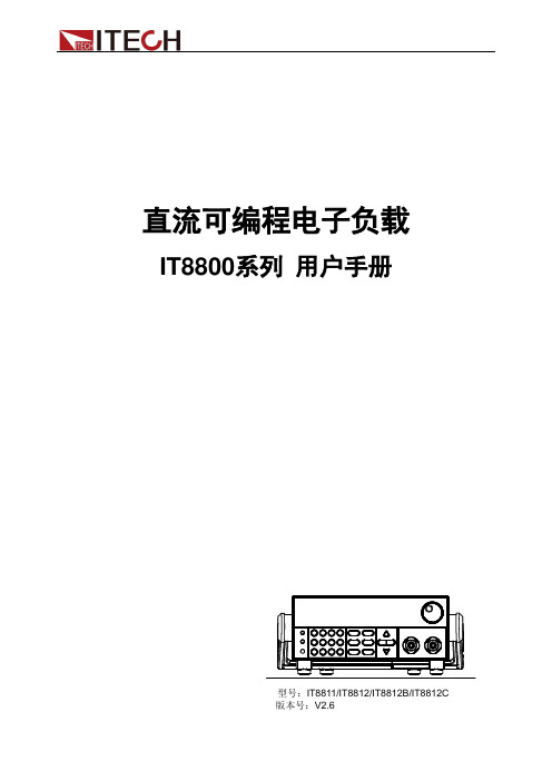
直流可编程电子负载IT8800系列用户手册型号:IT8811/IT8812/IT8812B/IT8812C版本号:V2.6声明© Itech Electronic, Co., Ltd. 2019根据国际版权法,未经Itech Electronic, Co., Ltd. 事先允许和书面同意,不得以任何形式(包括电子存储和检索或翻译为其他国家或地区语言)复制本手册中的任何内容。
手册部件号IT8800-402180版本第2版,2019 年10月15日发布Itech Electronic, Co., Ltd.商标声明Pentium是Intel Corporation在美国的注册商标。
Microsoft、Visual Studio、Windows 和MS Windows是Microsoft Corporation 在美国和/或其他国家/地区的商标。
担保本文档中包含的材料“按现状”提供,在将来版本中如有更改,恕不另行通知。
此外,在适用法律允许的最大范围内,ITECH 不承诺与本手册及其包含的任何信息相关的任何明示或暗含的保证,包括但不限于对适销和适用于某种特定用途的暗含保证。
ITECH对提供、使用或应用本文档及其包含的任何信息所引起的错误或偶发或间接损失概不负责。
如ITECH与用户之间存在其他书面协议含有与本文档材料中所包含条款冲突的保证条款,以其他书面协议中的条款为准。
技术许可本文档中描述的硬件和/或软件仅在得到许可的情况下提供并且只能根据许可进行使用或复制。
限制性权限声明美国政府限制性权限。
授权美国政府使用的软件和技术数据权限仅包括那些定制提供给最终用户的权限。
ITECH 在软件和技术数据中提供本定制商业许可时遵循FAR 12.211(技术数据)和12.212(计算机软件)以及用于国防的DFARS252.227-7015(技术数据-商业制品)和DFARS 227.7202-3(商业计算机软件或计算机软件文档中的权限)。
台湾艾德克斯IT8500帧格式通讯协议

IT8500 Series Frame FormatProgrammable DC Power SupplyModels IT8500© Copyright 2005 All Rights Reserved Ver1.1/MAR, 2008/8500-401DirectoryWarranty Information (3)Safety Summary (3)Chapter 1 Remote Operation Mode (5)1.1 IT-E131 RS232 Communication cable (5)1.2 IT-E132 USB Communication cable (5)Chapter 2 Communication Order for IT8500 (6)Frame Format (6)Communication Protocol (8)Warranty InformationCertificationWe certify that this product met its published specifications at time of shipment from the factory.WarrantyThis hardware product is warranted against defects in material and workmanship for a period of ONE year from date of delivery. IT8500 series electronic load for use with a hardware product and when properly installed on that hardware product, are warranted not to fail to execute their programming instructions due to defects in material and workmanship for a period of 90 days from date of delivery. During the warranty period our company will either repair or replace products which prove to be defective. Our company does not warranty that the operation for the software firmware or hardware shall be uninterrupted or error free.For warranty service, with the exception of warranty options, this product must be returned to a service facility designated by our company. Customer shall prepay shipping charges by (and shall pay all duty and taxes) for products returned to our place for warranty service. Our company shall pay for return of products to Customer.Limitation of WarrantyThe foregoing warranty shall not apply to defects resulting from improper or inadequate maintenance by the Customer, Customer-supplied software or interfacing, unauthorized modification or misuse, operation outside of the environmental specifications for the product, or improper site preparation and maintenance.AssistanceThe above statements apply only to the standard product warranty. Warranty options product maintenance agreements and customer assistance agreements are also available.Safety SummaryThe following general safety precautions must be observed during all phases of operation of this instrument. Failure to comply with these precautions or with specific warnings elsewhere in this manual violates safety standards of design, manufacture, and intended use of the instrument .We assumes no liability for the customer’s failure to comply with these requirements.Environmental ConditionsThis instrument is intended for indoor use. Pollution degree 2 environments. It is designed to operate at a maximum relative humidity of 95% and at altitudes of up to 2000 meters. Refer to the specifications tables for the ac mains voltage requirements and ambient operating temperature range.Before Applying PowerVerify that all safety precautions are taken. Note the instrument's external markings described under "Safety Symbols".Ground the InstrumentThis product is a Safety Class 1 instrument (provided with a protective earth terminal). To minimize shock hazard, the instrument chassis and cover must be connected to an electrical ground. The instrument must be connected to the ac power mains through a grounded power cable, with the ground wire firmly connected to an electrical ground (safety ground) at the power outlet. Note: Any interruption of the protective (grounding) conductor or disconnection of the protective earth terminal will cause a potential shock hazard that could result in personal injury.DO NOT OPERATE IN AN EXPLOSIVE ATMOSPHEREDo not operate the instrument in the presence of fumes or flammable gases.KEEP AWAY FROM LIVE CIRCUITSOperating personnel must not remove instrument covers except as instructed in this Guide for installing or removing electronic load modules. Component replacement and internal adjustments must be made only by qualified service personnel. Do not replace components with power cable connected. Under certain conditions dangerous voltages may exist even with the power cable removed. To avoid injuries always disconnect power, discharge circuits, and remove external voltage sources before touching components.DO NOT SERVICE OR ADJUST ALONEDo not try to do some internal service or adjustment unless another person capable of rendering first aid resuscitation is present.Safety SymbolsDirect currentAlternating currentBoth direct and alternating currentProtective earth (ground) terminalCaution (refer to accompanying documents)WARNINGThe WARNING sign denotes a hazard. It calls attention to a procedure, practice, or the like, which, if not correctly performed or adhered to, could result in personal injury. Do not proceed beyond a WARNING sign until the indicated conditions are fully understood and met.CAUTIONThe CAUTION sign denotes a hazard. It calls attention to an operating procedure, or the like, which, if not correctly performed or adhered to, could result in damage to or destruction of part or all of theChapter 1 Remote Operation ModeDB9 in the rear panel of electronic load could connect with RS-232 through on TTL connector. The following information may help you to know how to control the output of electronic load through PC.1.1 IT-E131 RS232 Communication cableThe DB9 interface connector on the rear panel of electronic load is TTL voltage level; you can use the communication cable (IT-E131) to connect the DB9 interface connector of the electronic load and the RS-232 interface connector of computer for the communication.PCLoadcableCOMPUTERI N S T R U M E N TRX TXIT1.2 IT-E132 USB Communication cableThe DB9 interface connector on the rear panel of electronic load is TTL voltage level; you can use the communication cable (IT-E132) to connect the DB9 interface connector of the electronic load and the USB interface connector of computer for the communication.PCLoadcableCOMPUTERI N S T R U M E N TRX TXITChapter 2 Communication Order for IT8500 Frame FormatFrame length is 26 bytes. Details as following:AAH Address Command 4—25bytes are information content Parity code Description :1. Start bit is AAH,occupies one byte.2.Address range from 0 to FE, occupies one byte.3.Each command occupies one byte. Following is the command details.20H Selecting the Remote control mode21H Selecting the input on/off state22H Setting the max input voltage23H Reading the max setup input voltage.24H Setting max input current25H Reading the max setup input current.26H Setting max input power.27H Reading the max setup input power.28H Selecting CC/CV/CW/CR operation mode of electronic load.29H Reading the operation mode.2AH Setting CC mode current value2BH Reading CC mode current value2CH Setting CV mode voltage value2DH Reading CV mode voltage value2EH Setting CW mode watt value2FH Reading CW mode watt value30H Setting CR mode resistance value31H Reading CR mode resistance value32H Setting CC mode transient current and timer parameter.33H Reading CC mode transient parameter34H Setting CV mode transient voltage and timer parameter.35H Reading CV mode transient parameter36H Setting CW mode transient watt and timer parameter37H Reading CW mode transient parameter38H Setting CR mode transient resistance and timer parameter39H Reading CR mode transient parameter3AH Selecting the list operation mode (CC/CV/CW/CR)3BH Reading the list operation mode.3CH Setting the list repeat mode (ONCE / REPEAT)3DH Reading the list repeat mode.3EH Setting the number of list steps.3FH Reading the number of list steps40H Setting one of the step’s current and time values.41H Reading one of the step’s current and time values.42H Setting one of the step’s voltage and time values.43H Reading one of the step’s voltage and time values44H Setting one of the step’s power and time values45H Setting one of the step’s power and time values.46H Setting one of the step’s resistance and time values47H Reading one of the step’s resistance and time values48H Setting list file name.49H Reading list file name.4AH Selection the memory space mode for storing list steps.4BH Reading the memory space mode for storing list steps.4CH Save list file in appointed area.4DH Get the list file from the appointed area.4EH Setting min voltage value in battery testing mode.4FH Reading min voltage value in battery testing mode50H Setting timer value of FOR LOAD ON51H Reading timer value of FOR LOAD ON52H Disable/Enable timer of FOR LOAD ON53H Reading timer state of FOR LOAD ON54H Setting communication address55H Enable/Disable LOCAL control mode.56H Enable/Disable remote sense mode.57H Reading the state of remote sense mode.58H Selecting trigger source.59H Reading trigger source.5AH Sending a trigger signal to trigging the electronic load.5BH Saving user’s setting value in appointed memory area for recall. 5CH Recall user’s setting value in appointed memory area.FIXED/SHORT/TRAN/LIST/BATTERY function mode. 5DH Selectingfunction mode state.5EH Getting5FH Reading input voltage, current, power and relative state60H Enter the calibration mode61H Getting the calibration mode state.62H Calibrate voltage value.63H Sending the actual input voltage to calibration program.64H Calibrate current value.65H Sending the actual input current to calibration program.66H Store the calibration data to EEPROM.67H Setting calibration information.68H Reading calibration information.69H Restore the factory default calibration data.6AH Reading product’s model, series number and version information.6CH Setting information of bar code12H The return information of command operation in electronic load.2. Selecting the input on/off state (21H)1st byte Start bit ( AAH )2nd byte Address(0—0XFE)3rd byte Command(21H)4th byte Input state(0 is OFF,1is ON)From 5th to 25th byte System reserveFrom26th byte Sum code3. Setting / Reading max input voltage(22H/23H)1st byte Start bit ( AAH )2nd byte Address (0—0XFE)3rd byte Command(22H/23H)4th byte The Lowest byte of max voltage value5th byte The lower byte of max voltage value.6th byte The higher byte of max voltage value.From 8th to 25th byte System reserve. 26th byte Sum code.6. Selecting / Reading CC/CV/CW/CR operation mode of electronic load.(28H/29H)1st byte Start bit ( AAH )2nd byte Address (0—0XFE)3rd byte Command(28H/29H)4th byte Mode(0 is CC mode, 1 is CV mode , 2 is CW mode , 3 is CR mode )From 5th to 25th byte System reserve26th byte Sum code7. Setting / Reading CC mode current value(2AH/2BH)1st byte Start bit ( AAH )2nd byte Address (0—0XFE)3rd byte Command (2AH/2BH)4th byte The lowest byte of current value5th byte The lower byte of current value.6th byte The higher byte of current value.7th byte The highest byte of current value.From 8th To 25th byte System reserve27th byte Sum code9. Setting / Reading CW mode watt value(2EH/2FH)1st byte Start bit ( AAH )2nd byte Address (0—0XFE)3rd byte Command(2EH/2FH)4th byte The lowest byte of max power value5th byte The lower byte of max power value6th byte The higher byte of max power value7th byte The highest byte of max power value8th to 25th byte System reserve26th byte Sum code11. Setting /Reading CC mode transient current and timer parameter. (32H/33H)1st byte Start bit ( AAH )2nd byte Address (0—0XFE)3rd byte Command(32H/33H)From 4th byte to 7th byte Setting value of current A (Lower bytes are in the front location, higher bytesare in the later location.)From 8th byte to 9th byte. Time value of timer A ((Lower bytes are in the front location, higher bytes are inthe later location) (1 represent 0.1mS)From 10th to 13th byte Setting value of current B (Lower bytes are in the front location, higher bytesare in the later location)the later location) (1 represent 0.1mS)16th byte Transition operation mode (0 is CONTINUES, 1 is PULSE, 2 is TOGGLED) From 17th to 25th byte System reserve26th byte Sum code12. Setting /Reading CV mode transient voltage and timer parameter.(34H/35H)1st byte Start bit ( AAH )2nd byte Address (0—0XFE)3rd byte Command(34H/35H)From 4th to 7th byte. Setting value of voltage A (Lower bytes are in the front location, higher bytesare in the later location)From 8th to 9th byte. Time value of timer A (Lower bytes are in the front location, higher bytes are inthe later location) (1represent 0.1mS)From 10th to 13th byte Setting value of voltage B(Lower bytes are in the front location, higher bytes arein the later location)From 14th to 15th byte Time value of timer B (Lower bytes are in the front location, higher bytes are inthe later location) (1represent 0.1mS)16th byte Transient operation mode (0 is CONTINUES,1 is PULSE,2 is TOGGLED) From 17th to 25th byte System reserve26th byte Sum code13. Setting /Reading CW mode transient watt and timer parameter(36H/37H)1st byte Start bit ( AAH )2nd byte Address (0—0XFE)3rd byte Command(36H/37H)From 4th to 7th byte Setting value of power A (Lower bytes are in the front location, higher bytes arein the later location)From 8th to 9th byte Time value of timer A (Lower bytes are in the front location, higher bytes are inthe later location) (1 represent 0.1mS)From 10th to 13th byte Setting value of power B(Lower bytes are in the front location, higher bytes arein the later location)From 14th to 15th byte Time value of timer B (Lower bytes are in the front location, higher bytes are inthe later location) (1 represent 0.1mS)16th byte Transition operation mode (0 is CONTINUES,1is PULSE,2 is TOGGLED) From 17th to 25th byte System reserve26th byte Sum code14. Setting /Reading CR mode transient resistance and timer parameter(38H/39H)1st byte Start bit ( AAH )2nd byte Address (0—0XFE)3rd byte Command(38H/39H)are in the later location)From 8th byte to 9th byte. Time value of timer A (Lower bytes are in the front location, higher bytes are inthe later location) (1 represent 0.1mS)From 10th byte to 13th byte Setting value of resistance B (Lower bytes are in the front location, higher bytesare in the later location)From 14th byte to 15th byte Time value of timer B (Lower bytes are in the front location, higher bytes are inthe later location) (1 represent 0.1mS)16th byte Transition operation mode (0 is CONTINUES,1 is PULSE,2 is TOGGLED)17th byte to 25th byte System reserve26th byte Sum code15.Selecting /Reading the list operation mode (CC/CV/CW/CR)(3AH/3BH)1st byte Start bit ( AAH )2nd byte Address (0—0XFE)3rd byte Command(3AH/3BH)4th byte LIST operation mode(0is CC mode,1 is CV mode ,2 is CW mode,3 is CR mode)From 5th to 25 byte System reserve26th byte Sum code16. Setting /Reading the list repeat mode. (3CH/3DH)1st byte Start bit ( AAH )2nd byte Address (0—0XFE)3rd byte Command(3CH/3DH)4th byte LIST repeat operation mode(0 is ONCE, 1 is REPEAT)From 5th to 25th byte System reserve26th byte Sum code17. Setting / Reading the number of list steps. (3EH/3FH)1st byte Start bit ( AAH )2nd byte Address (0—0XFE)3rd byte Command(3EH/3FH)From 4th to 5th byte LIST stepsFrom 6th to 25th byte System reserve26th byte Sum code18. Setting / Reading one of the step’s current and time values. (40H/41H)1st byte Start bit ( AAH )2nd byte Address (0—0XFE)3rd byte Command(40H/41H)From 4th byte to 5th byte Appointed one stepFrom 6th to 9th byte Current value of current step (Lower bytes are in the front location, higher bytesare in the later location)in the later location) (1 represent 0.1mS)From 12th to 25th byte System reserve26th byte Sum code19. Setting / Reading one of the step’s voltage and time values. (42H/43H)1st byte Start bit ( AAH )2nd byte Address (0—0XFE)3rd byte Command(42H/43H)From 4th to 5th byte Appointed one stepFrom 6th byte to 9th byte Voltage value of current step (Lower bytes are in the front location, higher bytesare in the later location)From 10th to 11th byte Time value of current step (Lower bytes are in the front location, higher bytes are in the later location) (1 represent 0.1mS)From 12th to 25th byte System reserve26th byte Sum code20. Setting / Reading one of the step’s power and time values. (44H/45H)1st byte Start bit ( AAH )2nd byte Address (0—0XFE)3rd byte Command(44H/45H)4th byte Appointed one stepFrom 5th to 8th byte Power value of current step (Lower bytes are in the front location, higher bytesare in the later location)From 9th to 10th byte Time value of current step (Lower bytes are in the front location, higher bytes are in the later location) (1 represent 0.1mS)From 11th to 25th byte System reserve26th byte Sum code21. Setting / Reading one of the step’s power and time values. (46H/47H)1st byte Start bit ( AAH )2nd byte Address (0—0XFE)3rd byte Command (46H/47H)From 4th to 5th byte Appointed one stepFrom 6th to 9th byte Resistance value of current step (Lower bytes are in the front location, higherbytes are in the later location)From 10th to 11th byte Time value of current step (Lower bytes are in the front location, higher bytes are in the later location) (1 represent 0.1mS)From 12th to 25th byte System reserve26th byte Sum code22. Setting / Reading List file name (48H/49H)1st byte Start bit ( AAH )2nd byte Address (0—0XFE)3rd byte Command (48H/49H)From 4th to 13th byte LIST file name (ASSIC code )From 14th to 25th byte System reserve26th byte Sum code23. Selection / Reading the memory space mode for storing list steps. (4AH/4BH) 1st byte Start bit ( AAH )2nd byte Address (0—0XFE)3rd byte Command(4AH/4BH)4th byte partition mode (1 | 2 | 4 | 8)From 5th to 25th byte System reserve26th byte Sum code24. Save / Get list file in appointed area.. (4CH/4DH)1st byte Start bit ( AAH )2nd byte Address (0—0XFE)3rd byte Command(4CH/4DH)4th byte Storing area 1 ~ 8)From 5th to 25th byte System reserve26th byte Sum code25. Setting / Reading min voltage value in battery testing mode.(4EH/4FH)1st byte Start bit ( AAH )2nd byte Address (0—0XFE)3rd byte Command(4EH/4FH)4th byte The lowest byte of voltage value.5th byte The lower byte of voltage value.6th byte The higher byte of voltage value.7th byte The highest byte of voltage value.From 8th to 25th byte System reserve26th byte Sum code26. Setting / Reading timer value of FOR LOAD ON (50H/51H)1st byte Start bit ( AAH )2nd byte Address (0—0XFE)3rd byte Command(50H/51H)4th byte The lowest byte of time value in timer. (1 represent 1S)5th byte The highest byte of time value in timer.From 8th to 25th byte System reserve26th byte Sum codeTime unit in Timer is S, 1S is represented by 1.27. Disable / Enable timer of FOR LOAD ON (52H);Reading timer state of FOR LOAD ON (53H)1st byte Start bit ( AAH )2nd byte Address (0—0XFE)3rd byte Command(52H/53H)4th byte Timer state (0 is disable ,1 is enable )From 5th to 25th byte System reserve26th byte Sum code28. Setting communication address (54H)1st byte Start bit ( AAH )2nd byte Address (0—0XFE)3rd byte Command (54H)4th byte New communication address (0~0XFE)From 5th to 25th byte System reserve26th byte Sum code29. Enable/Disable LOCAL control mode. (55H)1st byte Start bit ( AAH )2nd byte Address (0—0XFE)3rd byte Command (55H)4th byte State of LOCAL button(0:disable,1:enable “)From 5th to 25th byte System reserve26th byte Sum code30. Enable / Disable remote sense mode. (56H)Reading the state of remote sense mode. (57H)1st byte Start bit ( AAH )2nd byte Address (0—0XFE)3rd byte Command(56H/57H)4th byte Remote mode state (0:disable,1:enable)5th to 25th byte System reserve26th byte Sum code31. Selecting / Reading trigger source. (58H/59H)1st byte Start bit ( AAH )2nd byte Address (0—0XFE)3rd byte Command (58H/59H)4th byte Trigger mode (0:Keypad,1 External,mand)From 5th to 25th byte System reserve26th byte Sum code32. Sending a trigger signal to trigging the electronic load. (5AH) 1st byte Start bit ( AAH )2nd byte Address (0—0XFE)3rd byte Command(5AH)From 4th to 25th byte System reserve26th byte Sum code33. Saving / Recall user’s setting value in appointed memory area for recall.(5BH/5CH)1st byte Start bit ( AAH )2nd byte Address (0—0XFE)3rd byte Command(5BH/5CH)4th byte Storing area ( )From 5th to 25th byte System reserve26th byte Sum code34. Selecting / Getting FIXED/SHORT/TRAN/LIST/ BATTERY function mode.(5DH/5EH)1st byte Start bit ( AAH )2nd byte Address (0—0XFE)3rd byte Command(5DH/5EH)4th byte Work mode (0:FIXED,1:SHORT, 2:TRANSITION,3:LIST,4: BATTERY)From 5th to 25th byte System reserve26th byte Sum code35. Reading input voltage, current, power and relative state. (5FH)1st byte Start bit ( AAH )2nd byte Address (0—0XFE)3rd byte Command (5FH)From 4th to 7th byte Actual input voltage value (Lower bytes are in the front location, higher bytes are in the later location)From 8th to 11th byte Actual input current value (Lower bytes are in the front location, higher bytes arein the later location)From 12th to 15th byte Actual input power value (Lower bytes are in the front location, higher bytes arein the later location)16th byte Operation state registerFrom 17th to 18th byte Demand state registerFrom 19th to 25th byte System reserve26th byte Sum codeBIT SignalMeaning0 1 2 3 4 5 6 CALWTGREMOUTLOCALSENSELOTOperation state registerCalculate the new demarcate coefficientWait for trigger signalRemote control modeOutput stateLOCAL button state (0 is represent “not in effect “,1 is represent ‘in effect “)Remote testing modeFOR LOAD ON timer state0 1 2 3 4 5 6 7 8 9 RVOVOCOPOTSVCCCVCPCRDemand state registerInput reverse voltageOver voltageOver currentOver powerOver temperatureNot connect remote terminalConstant currentConstant voltageConstant powerConstant resistance36. Enter the calibration mode(60H)1st byte Start bit ( AAH )2nd byte Address (0—0XFE)3rd byte Command(60H)4th byte Calibration mode select(0:disable;1:enable) 5th byte Calibration password(0X85H)6th byte Calibration password(0X11H or 0X12H)From 7th to 25th byte System reserve26th byte Sum code38. Calibrate voltage value(62H)1st byte Start bit ( AAH )2nd byte Address (0—0XFE)3rd byte Command(62H)4th byte Voltage calibration point(1~4)From 5th to 25th byte System reserve26th byte Sum code41. Sending the actual input current to calibration program (65H)1st byte Start bit ( AAH )2nd byte Address (0—0XFE)3rd byte Command(65H)4th byte The lowest byte of actual current5th byte The lower byte of actual current6th byte The higher byte of actual current7th byte The highest byte of actual currentFrom 8th to 25th byte System reserve26th byte Sum code42. Store the calibration data to EEPROM(66H)1st byte Start bit ( AAH )2nd byte Address (0—0XFE)3rd byte Command (66H)From 4th to 25th byte System reserve26th byte Sum code45. Reading product’s model, series number and version information(6AH)1st byte Start bit ( AAH )2nd byte Address (0—0XFE)3rd byte Command(6AH)From 4th to 8th byte Mode information (ASIC code)9th byte The lowest byte of software version number(BCD code)10th byte The highest byte of software version number(BCD code)From 11th to 20th byte Product series number (ASIC code)From 21st to 25th byte System reserve26th byte Sum codeFor example:Product’s series number is 000045,product mode is 8511,software version number is V2.03,data as followingAA 00 31 38 35 31 31 00 03 02 ZZ ZZ ZZ ZZ ZZ ZZ ZZ ZZ ZZ ZZ XX XX XX XX XX 5746. Reading information in bar code (6BH)1st byte Start bit ( AAH )2nd byte Address (0—0XFE)3rd byte Command (6BH)From 4th to 22nd byte Information in bar code(ASICmode)From 23rd to 25th byte System reserve26th byte Sum code47. Setting information of bar code(6CH)1st byte Start bit ( AAH )2nd byte Address (0—0XFE)3rd byte Command(6CH)4th to 22nd byte Product series number(ASIC code)24th byte System reserve25th byte System reserve26th byte Sum code48. The return information of command operation in electronic load(12H)1st byte Start bit ( AAH )2nd byte Address (0—0XFE)3rd byte Command(12H)4th byte Command calibration resultFrom 5th to 25th byte System reserve26th byte Sum codeNOTEReceiving one frame command and verify themIf verify sum is wrong, return the parameter 90HIf setting parameter is wrong or over brim, return parameter A0H.If command is not enforce, return to parameter B0HIf command is invalid, return to parameter C0HOtherwise, return to parameter 80HNOTEReceiving one frame command and verify themIf verify sum is correct, return the relative reading dataIf verify sum is wrong, return the verify command (90H)。
电子负载仪器设备操作说明书
電子負載
電子負載
設備功能
功能測試
文件編號
設備型號
6312
廠 商
版 本
A0
1.各功能鍵功能說明﹕
1.1MODE模式轉換
1.2CLEAR 清除
1.3CHAN 功能選擇
1.4PROG 程序集
1.5RECALL 查詢
1.6SAVE 儲存
1.7SPEC 測試規格
1.8CONF 內置資料設定
1.9STACTIC/DYNA 動/靜態
3.5 工作時﹐可根據已儲存資料﹐按“RECALL”鍵﹐選擇所測項目﹔
3.6 工作完畢﹐按下“POWER”開關。
4.注意事項﹕
4.1 在使用過程中﹐“PRБайду номын сангаасG”, “CONF”鍵切勿操作﹔
4.2 儀器或治具出現異常時﹐非專業人員請勿亂操作﹐請與生技或儀保聯系。
核准
審核
制作
日期
2.操作說明﹕
2.1 根據提供電源﹐選擇電子負載電壓檔位﹔
2.2 按下“POWER”鍵,屏幕有數字顯示。
3.操作程序﹕
3.1 按“MODE”選擇“CCL”或“CCH”固定電流模式﹐按“ENTER”鍵根據提供電流大小﹐輸入數值﹐按“ENTER”鍵﹐再按“MODE”鍵﹔按“ENTER”鍵﹐然后按“SPEC”﹐輸入中心值(CENTER)﹐最大(HIGH)﹐最小(LOW)﹐最后按“SAVE”鍵輸入資料名﹐屏幕顯示“SAVE DEFAULT” 1:YES,2:NO﹐選擇數字1鍵﹐按“ENTER”再重復一次﹔
3.2 按動“LOAD”鍵﹐使其處于ON狀態﹐則負載當前處于滿載狀態﹐當為OFF狀態時為空載﹔
3.3 按動“SHORT”鍵﹐使其處于ON狀態﹐則負載當前處于短路狀態﹐反之則為開路狀態﹔
IT8500+ 编程与语法指南
安全声明
小心标志表示有危险。它要求在 执行操作步骤时必须加以注意, 如果不正确地执行或不遵守操作 步骤,则可能导致产品损坏或重 要数据丢失。在没有完全理解指 定的条件且不满足这些条件的情 况下,请勿继续执行小心标志所 指示的任何不当操作。
“警告 ”标志表示有危险。它要求 在执行操作步骤时必须加以注意, 如果不正确地执行操作或不遵守 操作步骤,则可能导致人身伤亡。 在没有完全理解指定的条件且不 满足这些条件的情况下,请勿继 续执行 “警告 ”标志所指示的任 何不当操作。
符合性信息
此部分列出一期遵循的 EMC(电磁兼容性)、安全和环境标准。
EC 一致性声明 – EMC
符合 Directive 2004/108/EC 有关电磁兼容性的要求。已证明符合《欧洲共同体
公报》中所列的以下技术规格:
EN 61326-1 2006: 测量、控制和实验室用电气设备的 EMC 要求。¹²³
安全注意事项
在此仪器操作的各个阶段中,必须遵循以下一般安全预防措施。如果未遵循这些 预防措施或本手册其他部分说明的特定警告,则会违反有关仪器的设计、制造和 用途方面的安全标准。 艾德克斯公司对用户不遵守这些预防措施的行为不承担 任何责任。
IT8500+系列电子负载支持 110V 或 220V 两种交流输入方式,请务必在开启电 源前检查电子负载的交流输入转换开关状态和供电电压相匹配,否则可能烧 坏电子负载
安全标志
直流电 交流电 既有直流也有交流电 保护性接地端子
ON(电源合) OFF(电源断) 电源合闸状态 电源断开状态
接地端子
参考端子
危险标志
正接线柱
警告标志(请参阅本手册了解 具体的“警告”或“小心”信 息)
艾德克斯IT8511_IT8512B_IT8512C电子负载仪说明书
代理艾德克斯电子负载/yiqi/itech/dianzifuzai.html 深圳格信达科技 电话18823303057 QQ:2104028976
代理艾德克斯电子负载/yiqi/itech/dianzifuzai.html 深圳格信达科技 电话18823303057 QQ:2104028976
ITECH艾德克斯电子负载仪IT8500系列单机直流电子负载
代理艾德克斯电子负载/yiqi/itech/dianzifuzai.html 深圳格信达科技 电话18823303057 QQ:2104028976
代理艾德克斯电子负载/yiqi/itech/dianzifuzai.html 深圳格信达科技 电话18823303057 QQ:2104028976
代理艾德克斯电子负载/yiqi/itech/dianzifuzai.html 深圳格信达科技 电话18823303057 QQ:2104028976
代理艾德克斯电子负载/yiqi/itech/dianzifuzai.html 深圳格信达科技 电话18823303057 QQ:2104028976
代理艾德克斯电子负载/yiqi/itech/dianzifuzai.html 深圳格信达科技 电话18823303057 QQ:2104028976
ห้องสมุดไป่ตู้
ITECH IT8500系列 说明书

版权归属于艾德克斯电子(南京)有限公司Ver3.0/Jan, 2010/ IT8500-401用户使用手册直流可编程电子负载本使用手册适用于下列机型型号 IT8511/IT8512/IT8512B/IT8512CIT8500系列第三章 面板操作 (13)3.1基本操作模式 ................................................ 13 3.1.1定电流操作模式(CC ) ............................................ 14 3.1.2定电阻操作模式(CR ) ............................................ 14 3.1.3定电压操作模式(CV ) ............................................ 14 3.1.4定功率操作模式(CW ) ............................................ 14 3.2动态测试操作 ................................................ 15 3.2.1连续模式(CONTINUOUS ) ....................................... 15 3.2.2脉冲模式(PULSE ) ............................................ 15 3.2.3触发模式(TRIGGER ) ............................................ 16 3.3顺序操作(LIST ) ............................................... 16 3.4 触发操作(TRIGGERED OPERATION ) ................................ 16 3.5 输入控制 ................................................ 17 3.5.1 短路操作(SHORT ) ............................................. 17 3.5.2 输入开关操作 ............................................. 17 3.6 电子负载可操作范围 ................................................. 17 3.7 保护功能 ................................................ 18 3.7.1 过电压保护(OV ) ............................................ 18 3.7.2 过电流保护(OC ) ............................................. 18 3.7.3 过功率保护(OW ) ............................................ 18 3.7.4 输入极性反接 ............................................. 18 3.7.5 过温度保护(OH ) .. (18)第二章 技术规格 .................................................. 12 2.1 主要技术参数 (12)2.2 补充特性 (13)第一章 快速入门 (6)1.1开机自检 ............................................... 6 1.1.1介绍 ............................................ 6 1.1.2自检步骤 ............................................ 6 1.1.3如果负载不能启动 ............................................ 6 1.2 前面板介绍 ................................................ 7 1.3后面板介绍 ................................................ 8 1.4 VFD 指示灯功能描述 ................................................ 8 1.5 键盘介绍 ................................................ 9 1.6快速功能键 ................................................ 9 1.7菜单操作 ................................................ 10 1.8选件和配件 (12)2用户使用手册目录第四章 安装 (21)4.1 验货 ................................................ 21 4.2清洁 ................................................ 21 4.3 安装位置 ................................................ 22 4.3.1 安装尺寸 ............................................. 22 4.3.2 负载把手的调节 ............................................. 23 4.3.3 支架安装 ............................................ 23 4.4 输入连接部分的安装 (25)第六章 负载通讯接口参考 (33)6.1通讯模块简介 ................................................. 33 6.2 电子负载与PC 间的通讯 (34)第五章 应用范例 (25)5.1 操作模式实例 25 5.1.1 定电流操作I-Set(设定一个从0到限定电流范围的定电流值) ........... 25 5.1.2 定功率操作P-Set (设定一个从0到限定功率范围的定功率值) ........... 26 5.1.3 定电阻操作R-set (设定一个从0.1Ω到4000Ω范围内定电阻值) ........... 26 5.1.4 定电压操作V-set (设定一个从0.1V 到限定电压范围的定电压值) ........... 26 5.1.5 IN ON/OFF 输入设定 ............................................. 26 5.2动态测试功能 ................................................ 26 5.2.1动态测试参数的设定 ............................................. 26 5.2.2动态测试操作 ............................................. 27 5.3顺序操作 ................................................ 29 5.4快速调用功能 ................................................ 30 5.5自动测试功能 ................................................ 30 5.5.1编辑测试档 ............................................. 30 5.5.2 快速取出测试档 ............................................. 31 5.5.3自动测试 ............................................. 32 5.6 电压量程和电流量程的快速切换方法 .. (32)3.8 远程测试功能 ................................................ 183.9 存取操作 ................................................ 193.10 电池放电测试操作 ................................................ 203.11 VON VOFF 操作 (20)3用户使用手册目录安全请勿自行在仪器上安装替代零件,或执行任何未经授权的修改。
艾德克斯多路电子负载操作指导书

1. 目的:为了使实验仪器操作方法规范,确保实验结果正确,延长仪器使用寿命,特制定本作业指导书。
2. 范围:本作业指导书适用该仪器的使用操作。
3. 职责:设备组:负责仪器定期校验。
实验室:负责仪器设备保养,作业指导书编写。
使用者:按照作业指导书使用仪器。
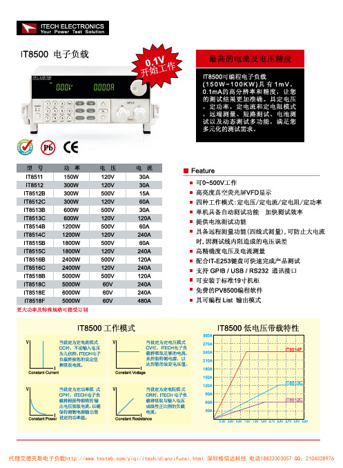
4. 作业内容:4.1. 仪器介绍4.1.1. 仪器主要参数IT8731: 输出电压80V 、 输出电流40A 、 输出功率200W 。
IT8733B: 输出电压500V 、输出电流30A 、 输出功率500W 。
IT8733: 输出电压80V 、 输出电流120A 、 输出功率600W 。
4.1.2. 仪器面板介绍4.1.3. 仪器按键功能介绍4.1.3.1. 控制模块按键功能介绍负载电源开关,打开时所有通道显示屏会点亮,所有通道进入开机自检的状态。
用来切换通道,由于IT8700是多路负载,一个主机控制所有模组。
每个模组都有自己的通道编号,想对某通道进行编辑,首先在主机面板上选择好编辑的通道才能进行编辑.例如:对5通道进行编辑,首先按Chan 键,主机VFD 上显示所有安装通道,直接按数字键5,就可以切换到5通道,这时就可以对该通道进行编辑。
用来保存数据,选择好通道后,在主机面板对该通道进行编辑参数,设置工作模式、电压、电流、斜率、动态参数等设置。
用101组设置参数。
所有的参数都保存在非易失性存储器中,可以掉电保存。
101组参数。
所有使用的参数只需要编辑和保存一次,它们就会一直保存在存储器中。
每次只需要调用即可。
用来进入单通道的菜单:此键用来单通道的菜单设置。
可实现A/B 动态的功能,选择CC/CV/CR 工作模式等,此菜单已在菜单列表中详细作了介绍。
/关闭:此键可以实现同步控制模组通道开启/关闭状态的功能。
只需要在配置菜单中开启所有模组的同步功能就可以。
触发功能键,编辑好自动测试文件或者动态脉冲输出时,必须选择触发源,负载有五种触发的方式,面板触发只是其中的一种。
- 1、下载文档前请自行甄别文档内容的完整性,平台不提供额外的编辑、内容补充、找答案等附加服务。
- 2、"仅部分预览"的文档,不可在线预览部分如存在完整性等问题,可反馈申请退款(可完整预览的文档不适用该条件!)。
- 3、如文档侵犯您的权益,请联系客服反馈,我们会尽快为您处理(人工客服工作时间:9:00-18:30)。
IT8500+用户手册
认证与质量保证
IT8500+系列电子负载完全达到手册中所标称的各项技术指标。
保固服务
ITECH 公司对本产品的材料及制造,自出货日期起提供一年的质量保固服务(保 固服务除以下保固限制内容)。
在此仪器操作的各个阶段中,必须遵循以下一般安全预防措施。如果未遵循这些 预防措施或本手册其他部分说明的特定警告,则会违反有关仪器的设计、制造和 用途方面的安全标准。 艾德克斯公司对用户不遵守这些预防措施的行为不承担任 何责任。
IT8500+系列电子负载支持 110V 或 220V 两种交流输入方式,请务必在开启 电源前检查电子负载的交流输入转换开关状态和供电电压相匹配,否则可能 烧坏电子负载
大短路输出电流而不会发生过热。如果有多个负载,则每对负载电线都必须 能安全承载电源的满载额定短路输出电流。 为减少起火和电击风险,请确保市电电源的电压波动不超过工作电压范围的 10%。 请勿自行在仪器上安装替代零件,或执行任何未经授权的修改。 请勿在可拆卸的封盖被拆除或松动的情况下使用本设备。 请仅使用制造商提供的电源适配器以避免发生意外伤害。 严禁将本设备使用于生命维持系统或其他任何有安全要求的设备上。
担保
本文档中包含的材料 “按现状 ”提 供,在将来版本中如有更改,恕不另 行通知。此外,在适用法律允许的最 大范围内,ITECH 不承诺与本手册 及其包含的任何信息相关的任何明 示或暗含的保证,包括但不限于对适 销和适用于某种特定用途的暗含保 证。 ITECH 对提供、使用或应用本 文档及其包含的任何信息所引起的 错误或偶发或间接损失概不负责。如 ITECH 与用户之间存在其他书面协 议含有与本文档材料中所包含条款 冲突的保证条款,以其他书面协议中 的条款为准。
保固服务不适用于因以下情况所造成的损坏:
顾客自行安装的电路造成的损坏,或顾客使用自己的产品造成的瑕疵; 顾客自行修改或维修过的产品; 顾客自行安装的电路造成的损坏或在指定的环境外操作本产品造成的损坏; 产品型号或机身序列号被改动、删除、移除或无法辨认; 由于事故造成的损坏,包括但不限于雷击、进水、火灾、滥用或疏忽。
若未按照制造商指定的方式使用设备,则可能会破坏该设备提供的保护。 请始终使用干布清洁设备外壳。请勿清洁仪器内部。 切勿堵塞设备的通风孔。
环境条件
IT8500+系列电子负载仅允许在室内以及低凝结区域使用,下表显示了本仪器的 一般环境要求。IT8500+系列电子负载风扇转速随散热器温度智能改变,当散热 器温度达到 40°C 时,风扇启动,随温度改变而智能调节。
安全标志
直流电 交流电 既有直流也有交流电 保护性接地端子
ON(电源合) OFF(电源断) 电源合闸状态 电源断开状态
接地端子
参考端子
危险 具体的“警告”或“小心”信息)
负接线柱
地线连接端标识
-
-
版权所有 © 艾德克斯电子有限公司
i
IT8500+用户手册
安全注意事项
直流可编程电子负载
IT8500+系列 用户手册
型号:IT8511+/IT8511A+/IT8512+/ IT8512A+/IT8512B+/IT8512C+/IT8512H+ /IT8513C+/IT8514C+/IT8514B+/IT8516C+
声明
© Itech Electronics, Co., Ltd. 2014 根据国际版权法,未经 Itech Electronics, I Co., Ltd. 事先允许和书面同意,不得以 任何形式(包括电子存储和检索或翻译为 其他国家或地区语言)复制本手册中的任 何内容。
手册部件号
IT8500+-402008
版本
第1版, 2014 年 11月 26 日发布 Itech Electronics, Co., Ltd.
商标声明
Pentium是 Intel Corporation在美国的注 册商标。
Microsoft、Visual Studio、Windows 和 MS Windows是 Microsoft Corporation 在美国和 /或其他国家 /地区的商标。
请勿使用已损坏的设备。在使用设备之前,请先检查其外壳。检查是否存在 裂缝或缺少塑胶。请勿在含有易爆气体、蒸汽或粉尘的环境中操作本设备。
电子负载出厂时提供了一个三芯电源线,您的电子负载应该被连接到三芯的 接线盒上。在操作电子负载供应器之前,您应首先确定电子负载接地良好!
请始终使用所提供的电缆连接设备。 在连接设备之前,请观察设备上的所有标记。 使用具有适当额定负载的电线,所有负载电线的容量必须能够承受电源的最
技术许可
本文档中描述的硬件和/或软件仅在得 到许可的情况下提供并且只能根据许可 进行使用或复制。
限制性权限声明
美国政府限制性权限。授权美国政府使用 的软件和技术数据权限仅包括那些定制 提供给最终用户的权限。ITECH 在软件 和技术数据中提供本定制商业许可时遵 循 FAR 12.211(技术数据)和 12.212 (计算机软件)以及用于国防的 DFARS 252.227-7015(技术数据-商业制品)和 DFARS 227.7202-3(商业计算机软件或 计算机软件文档中的权限)。
本产品若需保固服务或修理,请将产品送回 ITECH 公司指定的维修单位。
若需要送回 ITECH 公司作保固服务的产品,顾客须预付寄送到 ITECH 维修 部的单程运费,ITECH 公司将负责支付回程运费。
若从其它国家送回 ITECH 公司做保固服务,则所有运费、关税及其它税赋均 须由顾客负担。
保证限制
安全声明
小心标志表示有危险。它要求在 执行操作步骤时必须加以注意, 如果不正确地执行或不遵守操作 步骤,则可能导致产品损坏或重 要数据丢失。在没有完全理解指 定的条件且不满足这些条件的情 况下,请勿继续执行小心标志所 指示的任何不当操作。
“警告 ”标志表示有危险。它要求 在执行操作步骤时必须加以注意, 如果不正确地执行操作或不遵守 操作步骤,则可能导致人身伤亡。 在没有完全理解指定的条件且不 满足这些条件的情况下,请勿继 续执行 “警告 ”标志所指示的任 何不当操作。