nRF24LE1F16Q24 Schematic and Layout
毕业论文--智能小区车辆统计技术系统设计[管理资料]
![毕业论文--智能小区车辆统计技术系统设计[管理资料]](https://img.taocdn.com/s3/m/519362b0336c1eb91b375dd7.png)
1绪论随着社会经济的不断发展,国民生活水平的不断提高,兼具速度与舒适的车辆逐渐成为人们的代步工具。
然而对具有着各种大量车辆出入的小区物业而言,车辆的管理日益成为日常事务中的一项重要的工作内容。
由于车辆的激增,尤其是私家车数量的成倍增长,小区内交通堵塞、车辆擦挂等现象常有发生,小区内居民矛盾不断激化。
如何让管理人员了解小区内的车辆状况,对突发事件采取合适的措施,提高工作效率等就成了个小区物业期待解决的一个课题。
信息化是全球的趋势和潮流,是国家社会经济发展的必然选择。
在信息化和数字化的背景下小区物业车辆管理的信息化也将是不可阻挡的发展方向。
加快小区物业车辆管理车辆管理信息化的进程对改进现代化生活具有非同一般的意义。
智能小区车辆统计技术系统就是一款针对小区物业车辆管理的一套系统,它大大提高了小区物业车辆管理人员的工作效率,彻底改变了效率低下、漏洞百出的人工统计方式,也极大地减少了所需要的费用。
只要有车辆进出小区便会自动计数,并且当车辆达到小区所能容纳车辆的上限时便会自动报警,是一种能够为小区物业管理人员极大地减少工作量、节约成本的有效方式。
就当前车辆的数量以及未来国家的发展前景来看,人们对车辆仍然具有极大的需求,不得不说,小区车辆统计系统是一种颇有前景的管理方式。
小区车辆管理现状仍然有诸多问题,而我国目前车辆统计、计数系统只在大的工业环境及高速公路等有限场合存在,而忽略了与人民生活息息相关的小区车辆统计系统;即便个别小区具备了类似的系统而其昂贵的价格使得其难以推广。
因此迫切需要一种即经济实惠,又能解决这一问题的新的方法。
在进行了相关的调查了解后,我有了一些对于车辆统计计数的想法,查找了相关资料后发现,在现在的条件下这些想法是完全可以实现的。
本论文所研究的内容正好弥补了现阶段小区车辆统计的这一空白。
目前国内外在车辆检测系统中,大量应用了电磁传感技术、超声传感技术、视频检测技术、计算机技术、通信技术等高新科学技术。
NRF24LE1_CN简介

立即发布市场联系人:Anne Strand电话:+47 22 51 10 62传真:+47 22 51 10 99电邮地址:Anne.Strand@nordicsemi.no网址:新产品: 2.4GHz超低功耗系统芯片,其中包含nRF24L01+收发器、8位微控制器和闪存Nordic半导体推出世界上最小、集成度最高的单片超低功耗2.4GHz无线系统芯片-nRF24LE1Nordic半导体的nRF24LE1在尺寸方面超过了以前的超低功率(ULP)系统芯片(SoC):它把产业界中最好的2.4GHz收发器核(nRF24L01+)和一个8位混合信号微控制器与闪存集成在一块芯片上,用于超低功耗无线系统。
这个独一无二的芯片使用QFN封装,尺寸为4×4mm,是目前尺寸最小的单片超低功耗无线解决办法。
对于迅速发展的超低功耗无线市场,nRF24LE1是理想的芯片,因为它能够在一块芯片上运行RF协议堆栈和应用层。
挪威奥斯陆-2008年9月9日-Nordic半导体(奥斯陆证件交易所代号:NOD)今日推出nRF24LE1,这是2.4GHz的超低功耗无线系统芯片,用这个办法时,只需要一块芯片就可以实现无线应用系统。
用于超低功耗无线通信的系统芯片在nRF24LE1中,集成了一个功能齐全的2.4GHz收发器核nRF24L01+,并且包含Nordic公司经过实用证明的Enhanced ShockBurst™型硬件链接层。
nRF24LE1的最大电流很小,可以用钮扣电池供电,真正地实现了超低功耗。
在nRF24LE1中,还有一个加强型8051混合信号微控制器核,与以前的8051器件相比,它执行一条指令的时钟周期较少。
大多数指令只需要一个或者两个时钟周期,因而按照MIPS(每秒百万条指令)测试标准,它的性能平均提高了8倍。
这个优异性能与芯片上的16KB闪存和1KB的SRAM结合起来,保证了这个处理平台足以运行RF协议栈和应用层,而且运行起来十分容易。
nrf24l01(2.4G模块)

NRF24L01(2.4G模块)一、模块简介(1)2.4GHz全球开放ISM频段免许可证使用。
(2)最高工作速率2Mbps,高效GFSK调制,抗干扰能力强。
(3)126频道,满足多点通信和跳频通信需要。
(4)内置硬件CRC检错,和点对点通信地址控制。
(5)低功耗,1.9-3.6V工作,待机模式下22uA;掉电模式900nA。
(6)内置2.4GHz天线,体积小巧:15mm×29mm。
(7)模块可软件设置地址,只有收到本机地址时才会输出数据(提供中断提示),可直接接各种单片机使用,软件编程非常方便。
(8)内稳压电路,使用各种电源包括DC/DC开关电源均有很好的通道效果。
(9)2.54mm间距接口,DIP封闭。
(10)工作于Enhanced ShockBurst具有Automatic packet handling,Auto packet transaction handling,具有可选的内置包应答机制,极大地降低丢包率。
(11)与51单片机P0口连接的时候,需要加10K的上拉电阻,与其余口连接不需要。
(12)其他系列的单片机,如果是5V的,请参考该系列单片机IO口输出电流大小,如果超过10mA,需要串联电阻分压,否则容易烧毁模块!如果是3.3V的,可以直接和RF24L01模块的IO口线连接。
比如AVR系列单片机。
如果是5V的一般串接2K的电阻。
二、接口电路说明:1)VCC脚接电压范围为:1.9V-3.6V,不能在这个敬意之外,超过3.6V将会烧毁模块。
推荐电压3.3左右。
2)除电源VCC和接地端,其余脚都可以直接和普通的5V单片机IO口直接相连,无需转换。
当然对3V左右的单片机更加适用了。
3)硬件上面没有SPI的单片机也可以控制本模块,用普通单片机IO口模拟SPI,不需要单片机真正的串口介入,只需要普通的单片机IO口就可以了,当然用串口也可以。
4)如果需要其他封装接口,比如密脚插针,或者其他形式的接口,可联系我们定做。
nRF24LE1H 详细编程电路图 烧写电路
nRF24LE1 Flash/OTP Programming Adapter Kit User Guide Liability disclaimer
Nordic Semiconductor ASA reserves the right to make changes without further notice to the product to improve reliability, function or design. Nordic Semiconductor ASA does not assume any liability arising out of the application or use of any product or circuits described herein.
Figure 1. Kit content nRF24LE1 Flash/OTP Programming Adapter Kit content: • • 1 Programming Adapter Module 1 Printed Getting Started Guide
Revision 1.1
Main office: Otto Nielsens veg 12 7004 Trondheim Norway Phone: +47 72 89 89 00 Fax: +47 72 89 89 89
Revision History
Date December 2011 October 2009 Version 1.1 1.0 Description Removed references to the CD User Guide
nRFgo nRF24LE1 Flash/OTP Programming Adapter Kit
nRF24LE1芯片简单介绍

nRF24LE1芯片简单介绍NRF24LE1特性NRF24LE1采用了NORDIC最新的无线和超低功耗技术,在一个极小封装中集成了包括2.4G无线传输,增强型51 FLASH高速单片机,丰富外设及接口等的单片FLASH芯片,是一个综合了性能及成本的完美结合,很适合应用于各种2.4G的产品设计。
NRF24LE1=2.4GHz+Flash51+ADC+PWM+I2C+RTC+WDT+RNG+AES++COMP+UART+SPI….应用:无线鼠标,无线键盘,无线摇杆,PC外设,玩具,RFID,无线遥控,医学参数监测,线数字语音,工业控制及无线数据采集主要特性:1、内嵌 2.4GHz低功耗无线收发内核NRF24L01+, 250kbps,1Mbps,2Mbps空中速率2、高性能51内核,16kbytes Flash,1Kbyte data RAM,1Kbyte NVRAM3、具有丰富的外设资源,内置128bit AES硬件加密,32位硬件乘除处理器,6-12位ADC,两路PWM,I2C,UART,硬件随机数产生器件,WDT,RTC,模拟比较器4、提供QFN24,QFN32,QFN48多种封装,提供灵活应用选择5、灵活高效的开发手段,支持Keil C,ISP下载,是开发无线外设,RFID,消费产品,无线数传等有力工具及平台。
带Gazell协议Gazell协议是NORDIC专为2.4G无线桌面和其他无线应用设计推出的无线通信协议,配合NRF24LE1/NRF24LU1P使用,客户可以专注于应用设计,无需花费大量的精力在无线链路上。
低功耗Gazell协议是低功耗协议,可设计为纽扣电池供电的应用。
抗干扰性Gazell协议完成自动跳频及抗干扰的无线通信,具有在复杂环境下优异的抗干扰性能。
低延时Gazell协议充分利用NRF高速通信的特性,具有低延时特性,特别满足PC周边及其他应用。
高安全性Gazell协议具有AES 128bit 高强度加密,确保数据传输的安全可靠。
NRF24L01详细教程
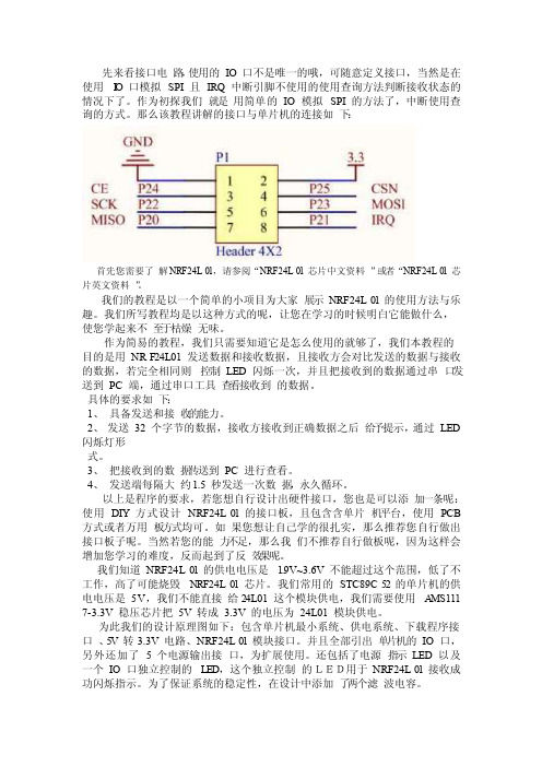
先来看接口电路,使用的IO 口不是唯一的哦,可随意定义接口,当然是在使用 I O 口模拟SPI 且IRQ 中断引脚不使用的使用查询方法判断接收状态的情况下了。
作为初探我们就是用简单的IO 模拟SPI 的方法了,中断使用查询的方式。
那么该教程讲解的接口与单片机的连接如下:首先您需要了解NRF24L01,请参阅“NRF24L01 芯片中文资料”或者“NRF24L01 芯片英文资料”。
我们的教程是以一个简单的小项目为大家展示NRF24L01 的使用方法与乐趣。
我们所写教程均是以这种方式的呢,让您在学习的时候明白它能做什么,使您学起来不至于枯燥无味。
作为简易的教程,我们只需要知道它是怎么使用的就够了,我们本教程的目的是用NRF24L01发送数据和接收数据,且接收方会对比发送的数据与接收的数据,若完全相同则控制LED 闪烁一次,并且把接收到的数据通过串口发送到PC 端,通过串口工具查看接收到的数据。
具体的要求如下:1、具备发送和接收的能力。
2、发送32 个字节的数据,接收方接收到正确数据之后给予提示,通过LED 闪烁灯形式。
3、把接收到的数据传送到PC 进行查看。
4、发送端每隔大约1.5 秒发送一次数据,永久循环。
以上是程序的要求,若您想自行设计出硬件接口,您也是可以添加一条呢:使用DIY 方式设计NRF24L01 的接口板,且包含含单片机平台,使用PCB 方式或者万用板方式均可。
如果您想让自己学的很扎实,那么推荐您自行做出接口板子呢。
当然若您的能力不足,那么我们不推荐自行做板呢,因为这样会增加您学习的难度,反而起到了反效果呢。
我们知道NRF24L01 的供电电压是 1.9V~3.6V 不能超过这个范围,低了不工作,高了可能烧毁 NRF24L01 芯片。
我们常用的STC89C52 的单片机的供电电压是5V,我们不能直接给24L01这个模块供电,我们需要使用 A MS1117-3.3V 稳压芯片把5V 转成3.3V 的电压为24L01 模块供电。
nRF24L01主要参数及电路图

nRF24L01 主要参数及电路图
nRF24L01 是由NORDIC 生产的工作在2.4GHz~2.5GHz 的ISM 频段的单片无线收发器芯片。
无线收发器包括:频率发生器、增强型SchockBurst 模式控制器、功率放大器、晶体振荡器、调制器和解调器。
输出功率频道选择和协议的设置可以通过SPI 接口进行设置。
几乎可以连接到各种单片机芯片,并完成无线数据传送工作。
极低的电流消耗:当工作在发射模式下发射功率为0dBm 时电流消耗为11.3mA ,接收模式时为12.3mA,掉电模式和待机模式下电流消耗更低。
nRF24L01 性能参数
小体积,QFN20 4x4mm 封装
宽电压工作范围,1.9V~3.6V,输入引脚可承受5V 电压输入。
nRF24E1英文

2.4Ghz RF transceiver with embedded8051 compatible microcontroller and 9 input, 10 bit ADC)($785(6•nRF2401 2.4GHz RF transceiver•8051 compatible microcontroller•9 input 10 bit ADC 100Kspls/s•Single 1.9V to 3.6V supply•Internal voltage regulators• 2 µA standby with wakeup ontimer or external pin•Internal VDD monitoring•Supplied in 36 pin QFN (6x6mm)package•7$%/( 2) &217(171GENERAL DESCRIPTION (4)1.1Quick Reference Data (4)1.2Block Diagram (5)1.3Pin Diagram (6)1.4Glossary of Terms (7)2ARCHITECTURAL OVERVIEW (8)2.1Microcontroller (8)2.2PWM (9)2.3SPI (9)2.4Port Logic (9)2.5Power Management (10)2.6RTC Wakeup Timer, Watchdog and RC Oscillator (10)2.7XTAL Oscillator (10)2.8AD Converter (10)2.9Radio Transceiver (11)3I/O PORTS (12)3.1I/O port behavior during RESET (12)3.2Port 0 (P0) (12)3.3Port 1 (P1 or SPI port) (13)4nRF2401 2.4GHz TRANSCEIVER SUBSYSTEM (16)4.1RADIO port (Port 2) (16)4.2Modes of operation (18)4.3Device configuration (24)4.4Data package Description (32)4.5Important RF Timing Data (33)5A/D CONVERTER (38)5.1A/D converter subsystem block diagram (38)5.2A/D converter registers (39)5.3A/D converter usage (40)6PWM (42)7INTERRUPTS (43)7.1Interrupt SFRs (43)7.2Interrupt Processing (46)7.3Interrupt Masking (47)7.4Interrupt Priorities (47)7.5Interrupt Sampling (48)7.6Interrupt Latency (48)7.7Interrupt Latency from Power Down State (48)7.8Single-Step Operation (48)8WAKEUP TIMER AND WATCHDOG (49)8.1Tick calibration (49)8.2RTC Wakeup timer (49)8.3Watchdog (50)8.4Reset (51)9POWER SAVING MODES (52)9.1Idle Mode (53)9.2Stop Mode (53)9.3Power down mode (53)10MICROCONTROLLER (55)10.1Memory Organization (55)10.2Program format in external EEPROM (56)10.3Instruction Set (57)10.4Instruction Timing (63)10.5Dual Data Pointers (63)10.6Special Function Registers (64)10.7SFR registers unique to nRF24E1 (67)10.8Timers/Counters (69)10.9Serial Interface (77)11ELECTRICAL SPECIFICATIONS (86)12PACKAGE OUTLINE (88)13ABSOLUTE MAXIMUM RATINGS (89)14Peripheral RF Information (90)15Table of Figures (91)16Table of Tables (91)17DEFINITIONS (94)*(1(5$/ '(6&5,37,21The nRF24E1 is a nRF2401 2.4GHz radio transceiver with an embedded 8051 compatible microcontroller and a 10-bit 9 input 100 kSPS AD converter. The circuit is supplied by only one voltage in range 1.9V to 3.6V. The nRF24E1 supports the proprietary and innovative modes of the nRF2401 such as ShockBurst™ and DuoCeiver™.4XLFN 5HIHUHQFH 'DWD3DUDPHWHU9DOXH8QLW Minimum supply voltage 1.9V Temperature range-40 to +85° C Maximum RF output power0dBmRF receiver sensitivity-90dBm Maximum RF burst data rate1000kbpsSupply current for microcontroller @ 16MHz @3V3mASupply current for ADC @100 kSPS0.9mASupply current for RF transmit @ -5dBm output power10.5mASupply current for RF receive18mASupply current in Power Down mode2µΑmax CPU clock frequency20MHzmax AD conversion rate100kSPSADC Differential nonlinearity (DNL)±0.5LSBADC Integral nonlinearity (INL)±0.75LSBADC Spurious free dynamic range (SFDR)65dB Package36 pin QFN 6x6Table 1-1 : nRF24E1 quick reference data7\SH 1XPEHU'HVFULSWLRQ9HUVLRQNRF24E1 IC36 pin QFN 6x6ANRF24E1-EVKIT Evaluation kit TBD 1.0 Table 1-2 : nRF24E1 ordering information%ORFN 'LDJUDPFigure 1-1 nRF24E1 block diagram plus external components3LQ 'LDJUDP',2 ',2 '9''',2',2 966;& ;&9669''$,1$,1$,1$5()$17$179''B3$9''',1 $,1 $,1 9669'',5()$,1 $,19663LQ1DPH3LQ IXQFWLRQ'HVFULSWLRQ1VDD Power Power Supply (1.9-3.6 V DC)2AIN0Analog input ADC input 03DVDD2RegulatedpowerDigital Power Supply , must be connected toregulator output DVDD4DIO0Digital I/O P1.0 (Port 1, bit 0)5DIO1Digital I/O P1.1 (Port 1, bit 1)6DIO2Digital I/O P0.0 (Port 0, bit 0)7DIO3Digital I/O P0.1 (Port 0, bit 1)8DIO4Digital I/O P0.2 (Port 0, bit 2)9DIO5Digital I/O P0.3 (Port 0, bit 3)10DIO6Digital I/O P0.4 (Port 0, bit 4)11DIO7Digital I/O P0.5 (Port 0, bit 5)12DIO8Digital I/O P0.6 (Port 0, bit 6)13DIO9Digital I/O P0.7 (Port 0, bit 7)14DVDD RegulatoroutputDigital voltage regulator output fordecoupling and feed to DVVD215VSS Power Ground (0V)16XC2Analog output Crystal Pin 217XC1Analog input Crystal Pin 118VDD_PA Regulatoroutput DC supply (+1.8V) to RF Power Amplifier (ANT1,ANT2) only19ANT1RF Antenna interface 120ANT2RF Antenna interface 221VSS_PA Power Ground (0V)22VDD Power Power Supply (1.9-3.6 V DC)23VSS Power Ground (0V)24AIN7Analog input ADC input 725AIN6Analog input ADC input 626AIN5Analog input ADC input 527IREF Analog input Connection to external Bias reference resistor 28AREF Analog input ADC reference voltage29AIN4Analog input ADC input 430AIN3Analog input ADC input 331VSS Power Ground (0V)32VDD Power Power Supply (1.9-3.6 V DC)33VSS Power Ground (0V)34AIN2Analog input ADC input 235AIN1Analog input ADC input 136DIN0Digital input P1.2 (Port 1, bit 2)Table 1-3 : nRF24E1 pin function*ORVVDU\ RI 7HUPV7HUP'HVFULSWLRQADC Analog to Digital ConverterCLK ClockCRC Cyclic Redundancy CheckCS Chip SelectCE Chip EnableDR Data ReadyGFSK Gaussian Frequency Shift KeyingGPIO General Purpose In OutISM Industrial-Scientific-MedicalkSPS kilo Samples per SecondMCU MicrocontrollerOD OverdriveP0 (or P1)(8051) In / Out Port 0 (or Port 1)PWM Pulse Width ModulationPWR_DWN Power DownPWR_UP Power UpRTC Real Time ClockRX ReceiveSFR(8051) Special Function RegisterSPI Serial Peripheral InterfaceST_BY StandbyTX TransmitXTAL Crystal (oscillator)$5&+,7(&785$/ 29(59,(:This section will give a brief overview of each of the blocks in the block diagram in Figure 1-1.0LFURFRQWUROOHUThe nRF24E1 microcontroller is instruction set compatible with the industry standard 8051. Instruction timing is slightly different from the industry standard, typically each instruction will use from 4 to 20 clock cycles, compared with 12 to 48 for the “standard”. The interrupt controller is extended to support 5 additional interrupt sources; ADC, SPI, RF receiver 1, RF receiver 2 and wakeup timer. There are also 3 timers which are 8052 compatible, plus some extensions, in the microcontroller core. An 8051 compatible UART that can use timer1 or timer2 for baud rate generation in the traditional asynchronous modes is included. The CPU is equipped with 2 data pointers to facilitate easier moving of data in the XRAM area, which is a common 8051 extension. The microcontroller clock is derived directly from the crystal oscillator.0HPRU\ FRQILJXUDWLRQThe microcontroller has a 256 byte data ram (8052 compatible, with the upper half only addressable by register indirect addressing). A small ROM of 512 bytes, contains a bootstrap loader that is executed automatically after power on reset or if initiated by software later. The user program is normally loaded into a 4k byte RAM1 from an external serial EEPROM by the bootstrap loader. The 4k byte RAM may also (partially) be used for data storage in some applications.%RRW ((3520 )/$6+If the mask ROM option is not used, the program code for the device must be loaded from an external non-volatile memory. The default boot loader expects this to be a “generic 25320” EEPROM with SPI interface. These memories are available from several vendors with supply ranges down to 1.8V. The SPI interface uses the pins DIN0 (EEPROM SDO), DIO0 (EEPROM SCK), DIO1 (EEPROM SDI) and DIO2 (EEPROM CSN). When the boot is completed, the DIN0, DIO0 and DIO1 pins may be used for other purposes such as other SPI devices or GPIO.5HJLVWHU PDSThe SFR (Special Function Registers) control several of the features of the nRF24E1. Most of the nRF24E1 SFRs are identical to the standard 8051 SFRs. However, there are additional SFRs that control features that are not available in the standard 8051. The SFR map is shown in the table below. The registers with grey background are registers with industry standard 8051 behavior. Note that the function of P0 and P1 are somewhat different from the “standard” even if the conventional addresses (0x80 and 0x90) are used1Optionally this 4k block of memory can be configured as 2k mask ROM and 2k RAM or 4 k mask ROM; ; ; ; ; ; ; ; ) EIP) B( EIE( ACC' EICON' PSW& T2CON RCAP2L RCAP2H TL2TH2&% IP T1_1V2T2_1V2DEV_OFFSET% RSTREAS SPI_DATASPI_CTRLSPICLKTICK_DVCK_CTRLTEST_MODE$ IE PWMCON PWMDUTYREGX_MSBREGX_LSBREGX_CTRL$ RADIO(P2)ADCCON ADCDATAHADCDATALADCSTATICSCON SBUFP1EXIF MPAGE P0_DIR P0_ALT P1_DIR P1_ALT TCON TMOD TL0TL1TH0TH1CKCON SPC_FNC P0SP DPL0DPH0DPL1DPH1DPS PCONTable 2-1 : SFR Register map3:0The nRF24E1 has one programmable PWM output, which is the alternate functionof PO.7 at pin DIO9.The resolution of the PWM is software programmable to 6, 7 or 8 bits.The frequency of the PWM signal is programmable via a 6 bit prescaler from the XTAL oscillator.The duty cycle is programmable between 0% and 100% via one 8-bit register.63,nRF24E1 features a simple single buffered SPI master. The 3 lines of the SPI bus (SDI, SCK and SDO) are multiplexed (by writing to register SPI_CTRL) between the GPIO pins (DIN0, DIO0 and DIO1) and the RF transceiver. The SPI hardware does not generate any chip select signal. The programmer will typically use GPIO bits (from port P0) to act as chip selects for one or more external SPI devices. When the SPI interfaces the RF transceiver, the chip selects are available in an internal GPIO port, P2.3RUW /RJLFThe device has 1 general purpose input and 10 general purpose bi-directional pins. These are by default configured as GPIO pins controlled by the ports P0 (DIO2 to DIO9) and P1 (DIO0, DIO1, DIN0) of the microcontroller.Most of the GPIO pins can be used for multiple purposes under program control. The alternate functions include two external interrupts, UART RXD and TXD, a SPI master port, three enable/count signals for the timers and the PWM output.3RZHU 0DQDJHPHQWThe nRF24E1 can be set into a low power down mode under program control, and also the ADC and RF subsystems can be turned on or off under program control. The CPU will stop, but all RAM’s and registers maintain their values. The low power RC oscillator is running, and so are the watchdog and the RTC wakeup timer (if enabled by software). The current consumption in this mode is typically 2µA.The device can exit the power down mode by an external pin interrupt (INT0_N or INT1_N) if enabled, by the wakeup timer if enabled or by a watchdog reset.57& :DNHXS 7LPHU :DWFKGRJ DQG 5& 2VFLOODWRUThe nRF24E1 contains a low power RC oscillator which can not be disabled, so it will run continuously as long as VDD 9RTC Wakeup Timer and Watchdog are two 16 bit programmable timers that run on the RC oscillator LP_OSC clock. The resolution of the watchdog and wakeup timer is programmable from approximately 300µs to approximately 80ms. By default the resolution is 10ms. The wakeup timer can be started and stopped by user software. The watchdog is disabled after a reset, but if activated it can not be disabled again, except by another reset;7$/ 2VFLOODWRUBoth the microcontroller, ADC and RF front end run on a crystal oscillator generated clock. A range of crystals frequencies from 4 to 20 MHz may be utilised, but 16 MHz is recommended since it gives best over all performance. For details, please see Crystal Specification on page 90. The oscillator may be started and stopped as requested by software.$' &RQYHUWHUThe nRF24E1 AD converter has 10 bit dynamic range and linearity with a conversion time of 48 CPU instruction cycles per 10-bit result.The reference for the AD converter is software selectable between the AREF input and an internal 1.22V bandgap reference.The converter has 9 inputs selectable by software. Selecting one of the inputs 0 to 7 will convert the voltage on the respective AIN0 to AIN7 pin.Input 8 enables software to monitor the nRF24E1 supply voltage by converting an internal input that is VDD/3 with the 1.22V internal reference selected.The AD converter is typically used in a start/stop mode. The sampling time is then under software control.The converter is by default configured as 10 bits. For special requirements, the AD converter can be configured by software to perform 6, 8 or 12 bit conversions. The converter may also be used in differential mode with AIN0 used as inverting input and one of the other 7 external inputs used as noninverting input. In that case the conversion time can be reduced to approximately 2 µs.5DGLR 7UDQVFHLYHUThe transceiver part of the circuit has identical functionality to the nRF2401 single chip RF transceiver. It is accessed through an internal parallel port and / or an internal SPI. The data ready signals for each DuoCeiver™ receiver output can be programmed as interrupts to the microcontroller or polled via a GPIO port.nRF2401 is a radio transceiver for the world wide 2.4 - 2.5 GHz ISM band. The transceiver consists of a fully integrated frequency synthesizer, a power amplifier, a modulator and two receiver units. Output power and frequency channels and other RF parameters are easily programmable by use of the RADIO register, SFR 0xA0. RF current consumption is only 10.5 mA in TX mode (output power -5dBm) and 18 mA in RX mode. For power saving the transceiver can be turned on / off under software control. Further information about the nRF2401 chip can be found at our website KWWS ZZZ QYOVL QR, 2 32576The nRF24E1 have two IO ports located at the default locations for P0 and P1 in standard 8051, but the ports are fully bi-directional CMOS and the direction of each pin is controlled by a _DIR and an _ALT bit for each bit as shown in the table below.Pin Default function Alternate=1SPI_CTRL=01DIN0P1.2SPI_DIDIO0P1.0T2 (timer2 input)SPI_SCKDIO1P1.1SPI_DODIO2P0.02EEPROM_CSNDIO3P0.1RXD (UART)DIO4P0.2TXD (UART)DIO5P0.3INT0_N(interrupt)DIO6P0.4INT1_N(interrupt)DIO7P0.5T0 (timer0 input)DIO8P0.6T1 (timer1 input)DIO9P0.7PWMTable 3-1 : Port functions, 2 SRUW EHKDYLRU GXULQJ 5(6(7During the period the internal reset is active (regardless of whether or not the clock is running), all the port pins are configured as inputs. When program execution starts, the DIO ports are still configured as inputs and the program will need to set the _ALT and/or the _DIR register for the pins that should be used as outputs.3RUW 3P0_ALT and P0_DIR control the P0 port function in that order of priority. If the alternate function for port p0.n is set (by P0_ALT.n = 1) the pin will be input or output as required by the alternate function (UART, external interrupt, timer inputs or PWM output), except that the UART RXD direction will still depend on P0_DIR.1.To use INT0_N or INT1_N, the corresponding alternate function must be activated,P0_ALT.3 / P0_ALT.4When the P0_ALT.n is not set, bit ‘n’ of the port is a GPIO function with the direction controlled by P0_DIR.n.P0.0 is always a GPIO. It will be activated by the default boot loader after reset and should be connected to the CSN of the boot flash.2Reserved for use as EEPROM_CSN, works as GPIO P0.0 independent of the “Alternate setting”'DWD LQ 3 B$/7 Q 3 B',5 Q3LQP0.0(DIO2)P0.0Out P0.0In P0.0Out P0.0InP0.1(DIO3)RXD Out RXD In P0.1Out P0.1InP0.2(DIO4)TXD Out TXD Out P0.2Out P0.2InP0.3(DIO5)INT0_N In INT0_N In P0.3Out P0.3InP0.4(DIO6)INT1_N In INT1_N In P0.4Out P0.4InP0.5(DIO7)T0In T0In P0.5Out P0.5InP0.6(DIO8)T1In T1In P0.6Out P0.6InP0.7(DIO9)PWM Out PWM Out P0.7Out P0.7In Table 3-2 : Port 0 (P0) functionsPort 0 is controlled by SFR-registers 0x80, 0x94 and 0x95 listed in the table below.$GGU 6)5 KH[ 5 : ELW,QLWKH[1DPH)XQFWLRQ80R/W8FF P0Port 0, pins DIO9 to DIO294R/W8FF P0_DIR Direction for each bit of Port 00: Output, 1: InputDirection is overridden if alternatefunction is selected for a pin.95R/W800P0_ALT Select alternate functions for each pin ofP0, if corresponding bit in P0_ALT is set,as listed in Table 3-2 : Port 0 (P0)functions, P0.0 has no alternatefunction,as it is intended as CS forexternal boot flash memory. It willfunction as a GPIO bit regardless ofP0_ALT.0Table 3-3 : Port 0 control and data SFR-registers3RUW 3 RU 63, SRUWThe P1 port consists of only 3 pins, one of which is an hardwired input. The function is controlled by SPI_CTRL.When SPI_CTRL is 01, the port is used as a SPI master port. The GPIO bits in port P0may be used as chip select(s).When not used as SPI port, P0_ALT.0 will force P1.0 to be the timer T2 input, P1.1 is now a GPIO. When P0_ALT.0 is 0, also P1.0 is a GPIO.P1.2 (DIN0) is always an input.63,B&75/3 B$/7 Q3LQ63,B&75/3 B$/7 Q3 B',5 Q 3 B',5 Q P1.0(DIO0)SCK Out T2In P1.0In P1.0Out P1.1(DIO1)SDO Out P1.1In 3P1.1In P1.1Out P1.2(DIN0)SDI In P1.2InP1.2InP1.2InTable 3-4 : Port 1 (P1) functionsPort 1 is controlled by SFR-registers 0x90, 0x96 and 0x97, and only the 3 lower bits of the registers are used.$GGU 6)5 KH[ 5 : ELW ,QLW KH[ 1DPH )XQFWLRQ90R/W 3FF P1Port 1, pins DIN0, DIO1 and DIO096R/W3FFP1_DIRDirection for each bit of Port 10: Output, 1: InputDirection is overridden if alternate function is selected for a pin, or if SPI_CTRL=01.bit0, DIN0 is always input.97R/W 300P1_ALT Select alternate functions for each pin of P1if corresponding bit in P1_ALT is set, as listed in Table 3-4 : Port 1 (P1) functions If SPI_CTRL is ‘01’, the P1 port is used as SPI master data and clock :2 -> MISO – input to nRF24E1 from slave 1 -> MOSI – output from nRF24E1 to slave 0 -> SCK – output from nRF24E1 to slaveTable 3-5 : Port 1 control and data SFR-registers3P1.1 is actually under control of P1_DIR.1 even when P1_ALT.1 is 1, since there is no alternatefunction for this pin.P1 may also be configured as a SPI master port , and is then controlled by the 3 SFR registers 0xB2, 0xB3, 0xB4 as shown in the table below.$GGU 6)5 KH[ 5:ELW,QLWKH[1DPH)XQFWLRQB2R/W80SPI_DATA SPI data input/outputB3R/W20SPI_CTRL00 -> SPI not used no clock generated01 -> SPI connected to port P1 (as for booting)another GPIO must be used as chip select(see also Table 3-4 : Port 1 (P1) functions)10 -> SPI connected to RADIOtransmitter/receiver 1 for TX or RX or fortransceiver configuration11 -> SPI connected to RADIO receiver 2 for RXChip select is a bit of RADIO register (seeTable 4-2 : RADIO register )B4R/W20SPICLK Divider factor from CPU clock to SPI clock00: 1/8 of CPU clock frequency01: 1/16 of CPU clock frequency10: 1/32 of CPU clock frequency11: 1/64 of CPU clock frequencyThe CPU clock is the oscillator generated clockdescribed in Crystal Specification page 90 Table 3-6 : SPI control and data SFR-registersQ5) *+] 75$16&(,9(5 68%6<67(05$',2 SRUW 3RUWThe transceiver is controlled by the RADIO port. The RADIO port uses the address normally used by port P2 in standard 8051. However since the radio transceiver is on chip, the port is not bi-directional. The power on default values in the port “latch” also differs from traditional 8051 to match the requirements of the radio transceiver subsystem.Operation of the transceiver is controlled by SFR registers RADIO and SPI_CTRL:$GGU 6)5 KH[ 5 : ELW,QLWYDOXHKH[1DPH)XQFWLRQA0R/W880RADIO General purpose IO for interface tonRF2401 radio transceiver subsystem B3R/W20SPI_CTRL00 -> SPI not used01 -> SPI connected to port P1 (boot)10 -> SPI connected to nRF2401 CH111 -> SPI connected to nRF2401 RXCH2Table 4-1 : nRF2401 2.4GHz transceiver subsystem control registers - SFR 0xA0 and 0xB3The bits of the RADIO register correspond to similar pins of the nRF2401 single chip, as shown in Table 4-2 : RADIO register . In the documentation the pin names are used, so please note that setting or reading any of these nRF2401 pins, means to write or read the RADIO SFR register accordingly. Please also note that in the transceiver documentation the notation MCU means the onchip 8051 compatible microcontroller. RADIO register bit corresponding pin name onsingle chip nRF24012.4GHz Transceiver5HDG7: 0 (not used)6: DR2, data ready from receiver 2 (available alsoas interrupt)DR25: CLK2, clock for receiver 2 data out CLK24: DOUT2, data out from receiver 2DOUT23: 0 (not used)2: DR1, data ready from receiver 1 (available alsoas interrupt)DR11: CLK1, clock for receiver 1 data out CLK10: DATA, data out from receiver 1DATA:ULWH7: PWR_UP, power on radio PWR_UP6: CE, Activate RX or TX mode CE5: CLK2, clock for receiver 2 data out CLK24: Not used3: CS, Chip select configuration mode CS2: Not used1: CLK1, clock for data input or receiver 1 data out CLK10: DATA, configuration or TX data input DATATable 4-2 : RADIO register - SFR 0xA0Note : Some of the pins are overridden when SPI_CTRL=1x, see Table 4-3 : Transceiver SPI interface.&RQWUROOLQJ WKH WUDQVFHLYHU YLD 63, LQWHUIDFHIt is more convenient to use the built-in SPI interface to do the most common transceiver operations as RF configuration and ShockBurst™ RX or TX. Please see Table 3-6 : SPI control and data SFR-registers for use of SPI interface. The radio port will be connected in different ways to the SPI hardware when SPI_CTRL is ‘1x’. When SPI_CTRL is ‘0x’, all radio pins are connected directly to their respective port pins.SPI signal SPI_CTRL=10 (binary)SPI_CTRL=11CS (active high)RADIO_wr.6 (CE) for ShockBurst™RADIO_wr.3 (CS) for ConfigurationRADIO_wr.6 (CE)SCK nRF2401/CLK1nRF2401/CLK2 SDI nRF2401/DATA nRF2401/DOUT2 SDO nRF2401/DATA not usedShockBurst™ data ready RADIO_rd.2 (DR1)RADIO_rd.6(DR2)Table 4-3 : Transceiver SPI interface.5$',2 SRUW EHKDYLRU GXULQJ 5(6(7During the period the internal reset is active (regardless of whether or not the clock is running), the RADIO outputs that control the nRF2401 transceiver subsystem are forced to their respective default values (RADIO.3=0 (CS), RADIO.6=0 (CE) RADIO.7=1 (PWR_UP)). When program execution starts, these ports will remain at those default levels until the programmer actively changes them by writing to the RADIO register.0RGHV RI RSHUDWLRQ2YHUYLHZThe nRF2401 subsystem can be set in the following main modes depending on three control pins:0RGH PWR_UP CE CSActive (RX/TX)110Configuration101Stand by100Power down0X XTable 4-4 nRF2401 subsystem main modes$FWLYH PRGHVThe nRF2401 subsystem has two active (RX/TX) modes:•ShockBurst™•Direct Mode (not supported by nRF24E1)The device functionality in these modes is decided by the content of a configuration word. This configuration word is presented in the configuration section. Please note that Direct mode is not supported, as this will require a more powerful CPU than 8051.6KRFN%XUVWThe ShockBurst™ technology uses on-chip FIFO to clock in data at a low data rateand transmit at a very high rate thus enabling extremely power reduction.When operating the nRF2401 subsystem in ShockBurst™, you gain access to the high data rates (1 Mbps) offered by the 2.4 GHz band without the need of a costly, high-speed microcontroller (MCU) for data processing.By putting all high speed signal processing related to RF protocol on-chip, thenRF24E1 offers the following benefits:•Highly reduced current consumption•Lower system cost (facilitates use of less expensive microcontroller)•Greatly reduced risk of ‘on-air’ collisions due to short transmission timeThe nRF2401 subsystem can be programmed using a simple 3-wire interface wherethe data rate is decided by the speed of the CPU.By allowing the digital part of the application to run at low speed while maximizingthe data rate on the RF link, the ShockBurst™ mode reduces the average current consumption in applications considerably.4.2.3.1ShockBurst™ principleWhen the nRF2401 subsystem is configured in ShockBurst™, TX or RX operation is conducted in the following way (10 kbps for the example only).TM1Mbps Figure 4-2Clocking in data with CPU and sending with ShockBurst™ technology020406080100120140160180200220240Time mSFigure 4-3 RF Current consumption with & without ShockBurst™ technologyData content of registers:Figure 4-4 Flow Chart ShockBurst™ Transmit of nRF2401 subsystem4.2.3.2ShockBurst™ Transmit:4.2.3.2.1CPU interface pins: CE, CLK1, DATA1.When the application CPU has data to send, set CE high. This activatesRF2401 on-board data processing.2.The address of the receiving node (RX address) and payload data isclocked into the nRF2401 subsystem. The application protocol or CPU setsthe speed <1Mbps (ex: 10kbps).3.CPU sets CE low, this activates a ShockBurst™ transmission.4.ShockBurst™:•RF front end is powered up•RF package is completed (preamble added, CRC calculated)•Data is transmitted at high speed (250 kbps or 1 Mbps configured by user).•nRF2401 subsystem returns to stand-by when finishedData content of registers:Figure 4-5 Flow Chart ShockBurst™ Receive of nRF2401 subsystem4.2.3.3 ShockBurst™ Receive:4.2.3.3.1 CPU interface pins: CE, DR1, CLK1 and DATA (one RX channel receive)1. Correct address and size of payload of incoming RF packages are set when nRF2401 subsystem is configured to ShockBurst™ RX.2. To activate RX, set CE high.3. After 200 µs settling, nRF2401 subsystem is monitoring the air for incoming communication.4. When a valid package has been received (correct address and CRC found),nRF2401 subsystem removes the preamble, address and CRC bits.5. nRF2401 subsystem then notifies (interrupts) the CPU by setting the DR1pin high.6. CPU may set the CE low to disable the RF front end (low current mode).7. The CPU will clock out just the payload data at a suitable rate (ex. 10kbps).8. When all payload data is retrieved nRF2401 subsystem sets DR1 low again, and is ready for new incoming data package if CE is kept high during data download. If the CE was set low, a new start up sequence can begin, see Figure 4-14. 'XR&HLYHU 6LPXOWDQHRXV 7ZR &KDQQHO 5HFHLYH 0RGHIn ShockBurst™ mode the nRF24E1 can facilitate simultaneous reception of two parallel independent frequency channels at the maximum data rate.This means:• nRF24E1 can receive data from two 1 Mbps transmitters (ex: nRF24E1,nRF2401 or nRF2402) 8 MHz (8 frequency channels) apart through one antenna interface.• The output from the two data channels is fed to two separate sets of interface pins.• Data channel 1: CLK1, DATA, and DR1• Data channel 2: CLK2, DOUT2, and DR2The DuoCeiver™ technology provides 2 separate dedicated data channels for RX andreplaces the need for two, stand alone receiver systems.Figure 4-6 Simultaneous 2 channel receive on nRF24E1There is one absolute requirement for using the second data channel. For the nRF24E1to be able to receive at the second data channel the frequency channel must be 8MHz higher than the frequency of data channel 1. The nRF2401 subsystem must be。