光伏发电外文翻译
光伏发电中英对照文献

外文参考文献译文及原文目录外文文献译文 (1)1.中国光伏发电的战略地位 (1)2.世界光伏产业现状和发展预测 (2)3.中国光伏发电市场和产业现状 (3)4.中国光复发电的市场预测和规划建议 (5)5.结论 (6)外文文献原文 (7)1.China's strategic position PV (7)2.The world's current situation and development of photovoltaic industryforecast (9)3.The Chinese PV market and industry statu s (10)4.China's PV market forecasting and planning proposals (13)5.Conclusions (15)外文文献译文1、中国光伏发电的战略地位1.1 中国的能源资源和可再生能源现状和预测;无论从世界还是从中国来看,常规能源都是很有限的,中国的一次能源储量远远低于世界的平均水平,大约只有世界总储量的10%。
从长远来看,可再生能源将是未来人类的主要能源来源,因此世界上多数发达国家和部分发展中国家都十分重视可再生能源对未来能源供应的重要作用。
在新的可再生能源中,光伏发电和风力发电是发展最快的,世界各国都把太阳能光伏发电的商业化开发和利用作为重要的发展方向。
根据欧洲JRC 的预测,到2030年太阳能发电将在世界电力的供应中显现其重要作用,达到10%以上,可再生能源在总能源结构中占到30%;2050 年太阳能发电将占总能耗的20%,可再生能源占到50%以上,到本世纪末太阳能发电将在能源结构中起到主导作用。
我国政府重视可再生能源技术的发展,主要有水能、风能、生物质能、太阳能、地热能和海洋能等。
我国目前可再生能源的发展现状如下:水能:我国经济可开发的水能资源量为3.9 亿千瓦,年发电量1.7 万亿千瓦时,其中5 万千瓦及以下的小水电资源量为1.25 亿千瓦。
太阳能发电外文翻译文献

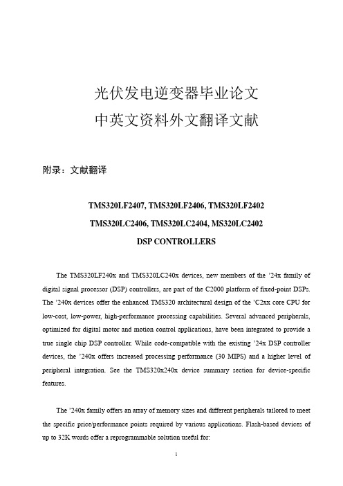
太阳能发电外文翻译文献(文档含中英文对照即英文原文和中文翻译)Design of a Lead-Acid Battery Charging and Protecting IC in Photovoltaic SystemZENG De-you,LING Chao-dong,LI Guo-gang1.IntroductionSolar energy as an inexhaustible, inexhaustible source of energy more and more attention. Solar power has become popular in many countries and regions, solar lighting has also been put into use in many cities in China. As a key part of the solar lighting, battery charging and protection is particularly important. Sealed maintenance-free lead-acid battery has a sealed, leak-free, pollution-free, maintenance-free, low-cost, reliable power supply during the entire life of the battery voltage is stable and no maintenance, the need for uninterrupted for the various typesof has wide application in power electronic equipment, and portable instrumentation. Appropriate float voltage, in normal use (to prevent over-discharge, overcharge, over-current), maintenance-free lead-acid battery float life of up to 12 ~ 16 years float voltage deviation of 5% shorten the life of 1/2. Thus, the charge has a major impact on this type of battery life. Photovoltaic, battery does not need regular maintenance, the correct charge and reasonable protection, can effectively extend battery life. Charging and protection IC is the separation of the occupied area and the peripheral circuit complexity. Currently, the market has not yet real, charged with the protection function is integrated on a single chip. For this problem, design a set of battery charging and protection functions in one IC is very necessary.2.System design and considerationsThe system mainly includes two parts: the battery charger module and the protection module. Of great significance for the battery as standby power use of the occasion, It can ensure that the external power supply to the battery-powered, but also in the battery overcharge, over-current and an external power supply is disconnected the battery is to put the state to provide protection, the charge and protection rolled into one to make the circuit to simplify and reduce valuable product waste of resources. Figure 1 is a specific application of this Ic in the photovoltaic power generation system, but also the source of this design.Figure1 Photovoltaic circuit system block diagramMaintenance-free lead-acid battery life is usually the cycle life and float life factors affecting the life of the battery charge rate, discharge rate, and float voltage. Some manufacturers said that if the overcharge protection circuit, the charging rate can be achieved even more than 2C (C is the rated capacity of the battery), battery manufacturers recommend charging rate of C/20 ~ C/3. Battery voltage and temperature, the temperature is increased by 1 °C, single cell battery voltage drops 4 mV , negative temperature coefficient of -4 mV / ° C means that the battery float voltage. Ordinary charger for the best working condition at 25 °C; charge less than the ambient temperature of 0 °C; at 45 °C may shorten the battery life due to severe overcharge. To make the battery to extend the working life, have a certain solar battery array Charge controllercontroller Dischargecontroller DC load accumulatorunderstanding and analysis of the working status of the battery, in order to achieve the purpose of protection of the battery. Battery, there are four states: normal state, over-current state over the state of charge, over discharge state. However, due to the impact of the different discharge current over-capacity and lifetime of the battery is not the same, so the battery over discharge current detection should be treated separately. When the battery is charging the state a long time, would severely reduce the capacity of the battery and shorten battery life. When the battery is the time of discharge status exceeds the allotted time, the battery, the battery voltage is too low may not be able to recharge, making the battery life is lower. Based on the above, the charge on the life of maintenance-free lead-acid batteries have a significant impact, while the battery is always in good working condition, battery protection circuit must be able to detect the normal working condition of the battery and make the action the battery can never normal working state back to normal operation, in order to achieve the protection of the battery.3.Units modular design3.1The charging moduleChip, charging module block diagram shown in Figure 2. The circuitry includes current limiting, current sensing comparator, reference voltage source, under-voltage detection circuit, voltage sampling circuit and logic control circuit.Figure2 Charging module block diagramdriverV oltage amplifierV oltage sampling comparatorStart amplifierState level control Charging indicator Logicalmodule Undervoltage detection circuitR- powerCurrent sampling comparator Limitingamplifier Power indicatorThe module contains a stand-alone limiting amplifier and voltage control circuit, it can control off-chip drive, 20 ~30 mA, provided by the drive output current can directly drive an external series of adjustment tube, so as to adjust the charger output voltage and current . V oltage and current detection comparator detects the battery charge status, and control the state of the input signal of the logic circuit. When the battery voltage or current is too low, the charge to start the comparator control the charging. Appliances into the trickle charge state when the cut-off of the drive, the comparator can output about 20 mA into the trickle charge current. Thus, when the battery short-circuit or reverse, the charger can only charge a small current, to avoid damage to the battery charging current is too large. This module constitutes a charging circuit charging process is divided into two charging status: high-current constant-current charge state, high-voltage charge status and low-voltage constant voltage floating state. The charging process from the constant current charging status, the constant charging current of the charger output in this state. And the charger continuously monitors the voltage across the battery pack, the battery power has been restored to 70% to 90% of the released capacity when the battery voltage reaches the switching voltage to charge conversion voltage Vsam charger moves to the state of charge. In this state, the charger output voltage is increased to overcharge pressure V oc is due to the charger output voltage remains constant, so the charging current is a continuous decline. Current down to charge and suspend the current Ioct, the battery capacity has reached 100% of rated capacity, the charger output voltage drops to a lower float voltage VF.3.2 Protection ModuleChip block diagram of the internal protection circuit shown in Figure 3. The circuit includes control logic circuit, sampling circuit, overcharge detection circuit, over-discharge detection comparator, overcurrent detection comparator, load short-circuit detection circuit, level-shifting circuit and reference circuit (BGR).Figure3 Block diagram of battery protectionThis module constitutes a protection circuit shown in Figure 4. Under the chip supply voltage within the normal scope of work, and the VM pin voltage at the overcurrent detection voltage, the battery is in normal operation, the charge and discharge control of the chip high power end of the CO and DO are level, when the chip is in normal working mode. Larger when the battery discharge current will cause voltage rise of the VM pin at the VM pin voltage at above the current detection voltage Viov, then the battery is the current status, if this state to maintain the tiov overcurrent delay time, the chip ban on battery discharge, then the charge to control the end of CO is high, the discharge control side DO is low, the chip is in the current mode, general in order to play on the battery safer and more reasonable protection, the chip will battery over-discharge current to take over the discharge current delay time protection. The general rule is that the over-discharge current is larger, over the shorter the discharge current delay time. Above Overcharge detection voltage, the chip supply voltage (Vdd> Vcu), the battery is in overcharge state, this state is to maintain the corresponding overcharge delay time tcu chip will be prohibited from charging the battery, then discharge control end DO is high, and charging control terminal CO is low, the chip is in charging mode. When the supply voltage of the chip under the overdischarge detection voltage (Vdd <Vdl,), then the battery is discharged state, this state remains the overdischarge delay time tdl chip will be prohibited to discharge the battery at this time The charge control side CO is high, while the discharge control terminal DO is low, the chip is in discharge mode. Sampling circuitOver discharge detection comparatorControl logic circuit Level conversion circuit Overcharge detection comparator Over-current detection comparator2 Over-current detection comparator1Over-current detection circuitLoad short detection circuitFigure4 Protection circuit application schematic diagram4.Circuit DesignTwo charge protection module structure diagram, the circuit can be divided into four parts: the power detection circuit (under-voltage detection circuit), part of the bias circuit (sampling circuit, the reference circuit and bias circuit), the comparator (including the overcharge detection /overdischarge detection comparator, over-current detection and load short-circuit detection circuit) and the logic control part.This paper describes the under-voltage detection circuit (Figure 5), and gives the bandgap reference circuit (Figure 6).Figure5 Under-voltage detection circuitProtectionmoduleBiasing circuit Reference circuit Bleeder circuit difference amplifier Output circuitAmplifierAmplifierFigure6 A reference power supply circuit diagramBattery charging, voltage stability is particularly important, undervoltage, overvoltage protection is essential, therefore integrated overvoltage, undervoltage protection circuit inside the chip, to improve power supply reliability and security. And protection circuit design should be simple, practical, here designed a CMOS process, the undervoltage protection circuit, this simple circuit structure, process and easy to implement and can be used as high-voltage power integrated circuits and other power protection circuit.Undervoltage protection circuit schematic shown in Figure 5, a total of five components: the bias circuit, reference voltage, the voltage divider circuit, differential amplifier, the output circuit. The circuit supply voltage is 10V; the M0, M1, M2, R0 is the offset portion of the circuit to provide bias to the post-stage circuit, the resistance, Ro, determine the circuit's operating point, the M0, M1, M2 form a current mirror; R1 M14 is the feedback loop of the undervoltage signal; the rest of the M3, M4 and M5, M6, M7, M8, M9, M10, M11, M12, M13, M14, composed of four amplification comparator; M15, DO, a reference voltage, the comparator input with the inverting input is fixed (V+), partial pressure of the resistance R1, R2, R3, the input to the inverting input of the comparator, when the normal working of the power supply voltage, the inverting terminal of the voltage detection is lost to the inverting terminal voltage of the comparator is greater than V+. Comparator output is low, M14 cutoff, feedback circuit does not work; undervoltage occurs, the voltage divider of R1, R2, R3, reaction is more sensitive, lost to the inverting input voltage is less than V when the resistor divider, the comparator the output voltage is high, this signal will be M14 open, the voltage across R into M at both ends of the saturation voltage close to 0V, thereby further driving down the R1> R2, the partial pressure of the output voltage, the formation of the undervoltage positive feedback. Output, undervoltage lockout, and plays a protective role.5. Simulation results and analysisThe design of the circuit in CSMC 0.6 μm in digital CMOS process simulation and analysis of the circuit. In the overall simulation of the circuit, the main observation is that the protection module on the battery charge and discharge process by monitoring Vdd potential and Vm potential leaving chip CO side and DO-side changes accordingly. The simulation waveform diagram shown in Figure 7, the overall protection module with the battery voltage changes from the usual mode conversion into overcharge mode, and then return to normal working mode, and then into the discharge mode, and finally back to normal working mode. As the design in the early stages of the various parameters to be optimized, but to provide a preliminary simulation results.Figure7 Overvoltage and under-voltage protection circuit simulation waveform6.ConclusionDesigned a set of battery charging and protection functions in one IC. This design not only can reduce the product, they can reduce the peripheral circuit components. The circuit uses the low-power design. This project is underway to design optimization stage, a complete simulation can not meet the requirements, but also need to optimize the design of each module circuit.光伏系统中蓄电池的充电保护IC电路设计曾德友,凌朝东,李国刚1.引言太阳能作为一种取之不尽、用之不竭的能源越来越受到重视。
太阳能行业专业术语中英文对照汇总
太阳能行业专业术语中英文对照汇总1. 太阳能发电系统 Solar Power Generation System2. 光伏板 Photovoltaic Panel3. 太阳能电池 Solar Cell4. 太阳辐射 Solar Radiation5. 光伏效率 Photovoltaic Efficiency6. 光伏薄膜 Photovoltaic Film7. 太阳能阵列 Solar Array8. 阳光能够转换的源能量 Potential Energy Converted by Sunlight9. 太阳能热发电 Solar Thermal Power Generation10. 光伏发电 Photovoltaic Power Generation11. 太阳能板 Solar Panel12. 逆变器 Inverter13. 太阳能光伏发电系统 Solar Photovoltaic Power Generation System14. 太阳能热水系统 Solar Water Heating System15. 太阳能电池组 Solar Battery Pack16. 漏电保护器 Leakage Protector17. 太阳能光伏电池组 Solar Photovoltaic Battery Pack18. 太阳能光伏电动车 Solar Photovoltaic Electric Vehicle19. 太阳能光伏发电机组 Solar Photovoltaic Power Generation Unit20. 太阳能发电塔 Solar Power Generation Tower21. 太阳能发电站 Solar Power Generation Plant22. 太阳能光伏逆变器 Solar Photovoltaic Inverter23. 太阳能电池板 Solar Cell Panel24. 太阳能电力系统 Solar Power System25. 碳排放 Carbon Emissions26. 绿色能源 Green Energy27. 可再生能源 Renewable Energy28. 太阳集热器 Solar Collector29. 太阳能集热器箱体 Solar Collector Box30. 太阳能热发电站 Solar Thermal Power Plant31. 太阳能发电设备 Solar Power Generation Equipment32. 光伏组件 Photovoltaic Module33. 太阳能光伏组件 Solar Photovoltaic Module34. 太阳能发电功率 Solar Power Generation Capacity35. 太阳能发电效益 Solar Power Generation Efficiency36. 太阳能热发电效率 Solar Thermal Power Generation Efficiency37. 太阳能供暖系统 Solar Heating System38. 太阳能温水器 Solar Water Heater39. 太阳能光伏装置 Solar Photovoltaic Device40. 太阳能热力系统 Solar Thermal System41. 太阳能电池片 Solar Cell Wafer42. 太阳能热发电板 Solar Thermal Power Generation Board43. 太阳能热发电效益 Solar Thermal Power Generation Benefit44. 太阳能热发电塔式反应器 Solar Thermal Power Generation Tower Reactor45. 光伏面板 Photovoltaic Panel46. 太阳能光伏面板 Solar Photovoltaic Panel47. 太阳能热板 Solar Thermal Plate48. 太阳能直驱泵 Solar Direct Drive Pump49. 太阳能冷水机组 Solar Cooling Unit50. 太阳能蓄电系统 Solar Battery Charging System。
光伏电站涉及专业英语词汇
(月度)等效停电时间
switching duration切换时间
E
energy能,电量
energy shortfall电量短缺
regulation energy of a system
系统的调节能量
estimation估计
slack bus松驰结点
voltage controlled bus电压控制母线
busbar节点,母线
reference busbar参考节点
C
calculation计算
load flow calculation负荷潮流计算
network calculation网络计算
power-flow calculation潮流计算
voltage deviation电压偏差
diagram图,图表
topological diagram of a network
网络拓扑图
droop下垂,衰减
droop of a system系统静特性
droop of a unit机组的静特性
duration(持续)时间,工作时间
(annual) equivalent interruption duration(年度)等效停电时间
series compensation串联补偿
shunt compensation并联补偿
under compensation欠补偿
controlling power range控制功率范围
power frequency control功率频率控制
voltage control电压控制
continuity连续性,持续性
光伏行业英文词汇
太阳电池 solar cell通常是指将太阳光能直接转换成电能的一种器件。
硅太阳电池silicon solar cell硅太阳电池是以硅为基体材料的太阳电池。
单晶硅太阳电池single crystalline silicon solar cell单晶硅太阳电池是以单晶硅为基体材料的太阳电池。
非晶硅太阳电池(a—si太阳电池)amorphous silicon solar cell用非晶硅材料及其合金制造的太阳电池称为非晶硅太阳电池,亦称无定形硅太阳电池,简称a—si太阳电池。
多晶硅太阳电池polycrystalline silicon solar cell多晶硅太阳电池是以多晶硅为基体材料的太阳电池。
聚光太阳电池组件photovoltaic concentrator module系指组成聚光太阳电池,方阵的中间组合体,由聚光器、太阳电池、散热器、互连引线和壳体等组成。
电池温度cell temperature系指太阳电池中P-n结的温度。
太阳电池组件表面温度solar cell module surface temperature系指太阳电池组件背表面的温度。
大气质量(AM)Air Mass (AM)直射阳光光束透过大气层所通过的路程,以直射太阳光束从天顶到达海平面所通过的路程的倍数来表示。
太阳高度角 solar 太阳高度角 solar elevation angle太阳光线与观测点处水平面的夹角,称为该观测点的太阳高度角。
辐照度 irradiance系指照射到单位表面积上的辐射功率(W/m2)。
总辐照(总的太阳辐照)total irradiation (total insolation)在一段规定的时间内,(根据具体情况而定为每小时,每天、每周、每月、每年)照射到某个倾斜表面的单位面积上的太阳辐照。
直射辐照度direct irradiance照射到单位面积上的,来自太阳圆盘及其周围对照射点所张的圆锥半顶角为8o的天空辐射功率。
光伏发电和风力发电混合发电系统论文中英文资料对照外文翻译文献综述
中英文资料对照外文翻译译文在混合光伏阵列中采用滑模技术的电源控制发电系统摘要变结构控制器来调节输出功率的一个独立的混合发电系统。
该系统包括光伏发电和风力发电,存储电池组和一个变量的单相负载。
控制律承认两种操作模式。
第一条用在当日晒度足够满足对电力的需求的情况下。
第二运作模式应用在日晒度不足的时候。
后者致使系统在最大功率操作点(MPOP)操作下存储尽可能多的能量。
根据IncCo nd算法开发的一种新方法。
滑模控制用于技术设计的控制律。
这些技术提供了一个简单的控制律设计框架,并有助于它们自带的鲁棒性。
最后,指导方针根据考虑为实际系统的设计。
1引言可再生能源,如风力和太阳能被认为是非常前途的能源。
它们拥有可以满足不断增加的世界能源需求的特点。
另一方面,他们是基于无公害转换流程,它们需要的主要资源是取之不尽,用之不竭,并且免费的。
对于远程、远离电网的地方,它往往是比用输电线路[1] 提供一个独立的电力来源拥有可行性。
在这些电网中,在混合动力系统结合模块的基础上,可再生能源发电以柴油为动力的备用发电机已考虑ERED等效为一个可行的选择[2, 3]。
然而,柴油发电机在孤立的燃料供应和其运作领域是相当麻烦,相比较可再生能源,显得不划算[4]。
为了取代柴油备用发电机,独立的混合动力系统经常采用结合可再生能源来源的TARY 型材,如风力和光伏发电,合适的存储设备,如电池。
自存储成本仍然是一个重大的经济约束,通常光伏/风能/电池系统是用“适当”的大小以减少资本成本。
本文提出了一种控制策略,以规范的混合动力系统,包括光伏发电和风力发电,蓄电池组和可变负载的输出功率作为研究。
控制可调整的光伏发电、风力发电,以满足负载和电池充电的电源要求。
系统以在独立控制下的最大发电的主要目标。
该控制器的设计开发,在之前的文献[5]中提过。
因此,根据不同的大气条件,不同的光伏阵列控制律使用的范围不同。
第一条用在暴晒的地方,运作模式足以提供的总功率需求,和风力发电一起适用。
光伏发电逆变器毕业论文中英文资料外文翻译文献
光伏发电逆变器毕业论文中英文资料外文翻译文献附录:文献翻译TMS320LF2407, TMS320LF2406, TMS320LF2402TMS320LC2406, TMS320LC2404, MS320LC2402DSP CONTROLLERSThe TMS320LF240x and TMS320LC240x devices, new members of the ‘24x family of digital signal processor (DSP) controllers, are part of the C2000 platform of fixed-point DSPs. The ‘240x devices offer the enhanced TMS320 architectural design of the ‘C2xx core CPU for low-cost, low-power, high-performance processing capabilities. Several advanced peripherals, optimized for digital motor and motion control applications, have been integrated to provide a true single chip DSP controller. While code-compatible with the existing ‘24x DSP controller devices, the ‘240x offers increased processing performance (30 MIPS) and a higher level of peripheral integration. See the TMS320x240x device summary section for device-specific features.The ‘240x family offers an array of memory sizes and different peripherals tailored to meet the specific price/performance points required by various applications. Flash-based devices of up to 32K words offer a reprogrammable solution useful for:◆Applications requiring field programmability upgrades.◆Development and initial prototyping of applications that migrate to ROM-baseddevices.Flash devices and corresponding ROM devices are fully pin-to-pin compatible. Note that flash-based devices contain a 256-word boot ROM to facilitate in-circuit programming.All ‘240x devices offer at least one event manager module which has been optimized for digital motor control and power conversion applications. Capabilities of this module include centered- and/or edge-aligned PWM generation, programmable deadband to prevent shoot-through faults, and synchronized analog-to-digital conversion. Devices with dual event managers enable multiple motor and/or converter control with a single ‗240x DSP controller.The high performance, 10-bit analog-to-digital converter (ADC) has a minimum conversion time of 500 ns and offers up to 16 channels of analog input. The auto sequencing capability of the ADC allows a maximum of 16 conversions to take place in a single conversion session without any CPU overhead.A serial communications interface (SCI) is integrated on all devices to provide asynchronous communication to other devices in the system. For systems requiring additional communication interfaces; the ‘2407, ‘2406, and ‘2404 offer a 16-bit synchronous serial peripheral interface (SPI). The ‘2407 and ‘2406 offer a controller area network (CAN) communications module that meets 2.0B specifications. To maximize device flexibility, functional pins are also configurable as general purpose inputs/outputs (GPIO).To streamline development time, JTAG-compliant scan-based emulation has been integrated into all devices. This provides non-intrusive real-time capabilities required to debug digital control systems. A complete suite of code generation tools from C compilers to the industry-standard Code Composerdebugger supports this family. Numerous third party developers not only offer device-level development tools, but also system-level design and development support.PERIPHERALSThe integrated peripherals of the TMS320x240x are described in the following subsections:●Two event-manager modules (EV A, EVB)●Enhanced analog-to-digital converter (ADC) module●Controller area network (CAN) module●Serial communications interface (SCI) module●Serial peripheral interface (SPI) module●PLL-based clock module●Digital I/O and shared pin functions●External memory interfaces (‘LF2407 only)●Watchdog (WD) timer moduleEvent manager modules (EV A, EVB)The event-manager modules include general-purpose (GP) timers, full-compare/PWM units, capture units, and quadrature-encoder pulse (QEP) circuits. EV A‘s and EVB‘s timers, compare units, and capture units function identically. However, timer/unit names differ for EV A and EVB. Table 1 shows the module and signal names used. Table 1 shows the features and functionality available for the event-manager modules and highlights EV A nomenclature.Event managers A and B have identical peripheral register sets with EV A starting at 7400h and EVB starting at 7500h. The paragraphs in this section describe the function of GP timers, compare units, capture units, and QEPs using EV A nomenclature. These paragraphs are applicable to EVB with regard to function—however, module/signal names would differ.Table 1. Module and Signal Names for EV A and EVBEVENT MANAGER MODULESEV AMODULESIGNALEVBMODULESIGNALGP Timers Timer 1Timer 2T1PWM/T1CMPT2PWM/T2CMPTimer 3Timer 4T3PWM/T3CMPT4PWM/T4CMPCompare Units Compare 1Compare 2Compare 3PWM1/2PWM3/4PWM5/6Compare 4Compare 5Compare 6PWM7/8PWM9/10PWM11/12Capture Units Capture 1Capture 2Capture 3CAP1CAP2CAP3Capture 4Capture 5Capture 6CAP4CAP5CAP6QEP QEP1QEP2QEP1QEP2QEP3QEP4QEP3QEP4External Inputs DirectionExternalClockTDIRATCLKINADirectionExternal ClockTDIRBTCLKINBGeneral-purpose (GP) timersThere are two GP timers: The GP timer x (x = 1 or 2 for EV A; x = 3 or 4 for EVB) includes:● A 16-bit timer, up-/down-counter, TxCNT, for reads or writes● A 16-bit timer-compare register, TxCMPR (double-buffered with shadow register), forreads or writes● A 16-bit timer-period register, TxPR (double-buffered with shadow register), forreads or writes● A 16-bit timer-control register,TxCON, for reads or writes●Selectable internal or external input clocks● A programmable prescaler for internal or external clock inputs●Control and interrupt logic, for four maskable interrupts: underflow, overflow, timercompare, and period interrupts● A selectable direction input pin (TDIR) (to count up or down when directionalup-/down-count mode is selected)The GP timers can be operated independently or synchronized with each other. The compare register associated with each GP timer can be used for compare function and PWM-waveform generation. There are three continuous modes of operations for each GP timer in up- or up/down-counting operations. Internal or external input clocks with programmable prescaler are used for each GP timer. GP timers also provide the time base for the other event-manager submodules: GP timer 1 for all the compares and PWM circuits, GP timer 2/1 for the capture units and the quadrature-pulse counting operations. Double-buffering of the period and compare registers allows programmable change of the timer (PWM) period and the compare/PWM pulse width as needed.Full-compare unitsThere are three full-compare units on each event manager. These compare units use GP timer1 as the time base and generate six outputs for compare and PWM-waveform generation using programmable deadband circuit. The state of each of the six outputs is configured independently. The compare registers of the compare units are double-buffered, allowing programmable change of the compare/PWM pulse widths as needed.Programmable deadband generatorThe deadband generator circuit includes three 8-bit counters and an 8-bit compare register. Desired deadband values (from 0 to 24 µs) can be programmed into the compare register for the outputs of the three compare units. The deadband generation can be enabled/disabled for each compare unit output individually. The deadband-generator circuit produces two outputs (with orwithout deadband zone) for each compare unit output signal. The output states of the deadband generator are configurable and changeable as needed by way of the double-buffered ACTR register.PWM waveform generationUp to eight PWM waveforms (outputs) can be generated simultaneously by each event manager: three independent pairs (six outputs) by the three full-compare units with programmable deadbands, and two independent PWMs by the GP-timer compares.PWM characteristicsCharacteristics of the PWMs are as follows:●16-bit registers●Programmable deadband for the PWM output pairs, from 0 to 24 µs●Minimum deadband width of 50 ns●Change of the PWM carrier frequency for PWM frequency wobbling as needed●Change of the PWM pulse widths within and after each PWM period as needed●External-maskable power and drive-protection interrupts●Pulse-pattern-generator circuit, for programmable generation of asymmetric,symmetric, and four-space vector PWM waveforms●Minimized CPU overhead using auto-reload of the compare and period registersCapture unitThe capture unit provides a logging function for different events or transitions. The values of the GP timer 2 counter are captured and stored in the two-level-deep FIFO stacks when selected transitions are detected on capture input pins, CAPx (x = 1, 2, or 3 for EV A; and x = 4, 5, or 6 for EVB). The capture unit consists of three capture circuits.Capture units include the following features:●One 16-bit capture control register, CAPCON (R/W)●One 16-bit capture FIFO status register, CAPFIFO (eight MSBs are read-only, eightLSBs are write-only)●Selection of GP timer 2 as the time base●Three 16-bit 2-level-deep FIFO stacks, one for each capture unit●Three Schmitt-triggered capture input pins (CAP1, CAP2, and CAP3)—one input pinper capture unit. [All inputs are synchronized with the device (CPU) clock. In order fora transition to be captured, the input must hold at its current level to meet two risingedges of the device clock. The input pins CAP1 and CAP2 can also be used as QEPinputs to the QEP circuit.]●User-specified transition (rising edge, falling edge, or both edges) detection●Three maskable interrupt flags, one for each capture unitEnhanced analog-to-digital converter (ADC) moduleA simplified functional block diagram of the ADC module is shown in Figure 1. The ADC module consists of a 10-bit ADC with a built-in sample-and-hold (S/H) circuit. Functions of the ADC module include:●10-bit ADC core with built-in S/H●Fast conversion time (S/H + Conversion) of 500 ns●16-channel, muxed inputs●Autosequencing capability provides up to 16 ―autoconversions‖ in a single session.Each conversion can be programmed to select any 1 of 16 input channels●Sequencer can be operated as two independent 8-state sequencers or as one large16-state sequencer (i.e., two cascaded 8-state sequencers)●Sixteen result registers (individually addressable) to store conversion values●Multiple triggers as sources for the start-of-conversion (SOC) sequence✧S/W – software immediate start✧EV A – Event manager A (multiple event sources within EV A)✧EVB – Event manager B (multiple event sources within EVB)✧Ext – External pin (ADCSOC)●Flexible interrupt control allows interrupt request on every end of sequence (EOS) orevery other EOS●Sequencer can operate in ―start/stop‖ mode, allowing multiple ―time-sequencedtriggers‖ to synchronize conv ersions●EV A and EVB triggers can operate independently in dual-sequencer mode●Sample-and-hold (S/H) acquisition time window has separate prescale control●Built-in calibration mode●Built-in self-test modeThe ADC module in the ‘240x has been enhanced to pro vide flexible interface to event managers A and B. The ADC interface is built around a fast, 10-bit ADC module with total conversion time of 500 ns (S/H + conversion). The ADC module has 16 channels, configurable as two independent 8-channel modules to service event managers A and B. The two independent 8-channel modules can be cascaded to form a 16-channel module. Figure 2 shows the block diagram of the ‘240x ADC module.The two 8-channel modules have the capability to autosequence a series of conversions,each module has the choice of selecting any one of the respective eight channels available through an analog mux. In the cascaded mode, the autosequencer functions as a single 16-channel sequencer. On each sequencer, once the conversion is complete, the selected channel value is stored in its respective RESULT register. Autosequencing allows the system to convert the same channel multiple times, allowing the user to perform oversampling algorithms. This gives increased resolution over traditional single-sampled conversion results.Figure 2. Block Diagram of the ‘240x ADC ModuleFrom TMS320LF2407, TMS320LF2406, TMS320LF2402TMS320LC2406, TMS320LC2404, MS320LC2402数字信号处理控制器TMS320LF240x和TMS320LC240x系列芯片作为’24x系列DSP控制器的新成员,是C2000平台下的一种定点DSP芯片。
太阳能专业英语翻译
Unit1 renewable Energy CommercializationIntroduction可再生能源商业化涉及可再生能源三代技术的部署要追溯到100多年,见图1.1和图1.2。
第一代技术已经成熟和经济竞争包括,生物量、水力发电、地热能和热。
第二代市场化技术目前正在部署,其中包括太阳能加热,光伏发电,风力发电、太阳能热发电站和现代形式的生物能源。
第三代技术需要继续努力研究和开发(研发)为了在全球范围内,做出巨大的贡献。
先进的生物质气化技术、包括干热岩地热发电,海洋能发电.有一些非技术性的障碍广泛存在于可再生能源,而且往往是公共政策和政治领导,帮助解决这些障碍,推动可再生能源技术的更广泛的利用。
2010年,98个国家制定自己的可再生能源期货目标和制定广泛的公共政策来提倡可再生能源。
而且气候变化的问题推动了可再生能源行业的增长。
领先的可再生能源公司包括第一太阳能、Gamesa、通用电气能源,q - cells,锋利太阳能、西门子、Sunopta尚德和维斯塔斯。
可再生能源的总投资在2010亿年达到211亿美元,高于在2009年的160亿美元。
2010年投资最多的国家是中国、德国、美国、意大利和巴西。
预计可再生能源行业的持续增长和与许多其他行业相比在2009年经济危机中促销政策能帮助天气行业。
美国总统奥巴马在2009年美国复苏与再投资法案中包括再投资700亿美元的支出和抵免税收对清洁能源和相关的运输计划。
清洁科技表明,清洁能源的商业化已经帮助世界各国摆脱2009年的全球金融危机。
经济分析师预计市场可再生能源(天然气)收益在2011年日本核事故直接影响了在全球范围内可再生能源行业中大约300万个工作岗位,其中大约一半是生物燃料产业。
根据国际能源署2011年的推测, 在50年内太阳能发电机可能产生世界上大多数的电力,显著降低有害温室气体的排放。
Lesson1 overviewRationale for renewables气候变化、污染和能源安全是当前最严重的问题和解决他们需要能量基础设施的重大改变。
- 1、下载文档前请自行甄别文档内容的完整性,平台不提供额外的编辑、内容补充、找答案等附加服务。
- 2、"仅部分预览"的文档,不可在线预览部分如存在完整性等问题,可反馈申请退款(可完整预览的文档不适用该条件!)。
- 3、如文档侵犯您的权益,请联系客服反馈,我们会尽快为您处理(人工客服工作时间:9:00-18:30)。
附录A 英文文献1.The world's current situation and development of photovoltaic industry forecastSolar cells is the use of the material effects of photovoltaic solar energy into electrical energy directly to the semiconductor devices, also known as photovoltaic cells. In 1954, the first practical silicon solar cells (η = 6%) and the first atomic power station at the same time in the United States was born in 1959 into the space solar cell applications, the energy crisis in 1973 after the application step by step to the ground.Photovoltaic power generation is divided into independent grid photovoltaic systems and photovoltaic systems. Independent PV power station, including the villages in remote areas the power supply system, solar household power system, communications, signal power, cathodic protection, such as solar street lamps withbatteries can run independently of the photovoltaic power generation system.Grid PV system is connected with the power grid to feed electricity grid PV power system. Currently technically achievable grid PV power system in the way: housing fixed-grid system and power plant system of the desert. Use of the existing roof system is the effective area of the roof construction, installation and network of photovoltaic power generation system, the size of a few kWp generally ranging from several MWp. Desert power plant is uninhabited desert area in the development and construction of large-scale photovoltaic power generation systems and networks, the size of several GWp from the 10MWp size. In recent years, the rapid increase in solar cell production, for 8 years in 30% growth in 2004, even more than the annual growth rate of 60 percent, reaching 1200MW.2.The Chinese PV market and industry status2.1 China's solar market developmentChina started research on solar cells in 1958, in 1971, China successfully launched the first applies to the 2nd satellite Dongfanghong. Started in 1973 for ground-based solar cells. China's photovoltaic industry in 80 years ago is still in embryonic form, the annual production of solar cells has been hovering below 10KW, price is also very expensive.As a result of restrictions on prices and production, market development is very slow, and apart from, as the satellite power supply, on the ground only for low-power solar power systems, such as beacon lights, railway signal systems, weather station equipment alpine electricity, electricity Wai field, black light, fluorescent lamps, such as DC power is normally a few watts to tens of watts. In the "65" (1981-1985) and "75" (1986-1990), the countries of photovoltaic PV industry and to give support for the development of the market, the central and local governments invested in the photovoltaic certain funds, makes a very weak solar industry hasbeen consolidated and applied in many areas of the model, such as microwave relay stations, communications system units, gates and oil pipeline cathodic protection systems, rural carrier telephone system, small households and villages with power supply system systems. At the same time, "75" period, the domestic has introduced from abroad a number of solar cell production line, in addition to the amorphous silicon, a 1MW battery production line, the other is single crystal silicon cell production line, making China's solar cell production capacity increased to 4.5MWp / years, the price is also from "75" early 80 yuan / Wp dropped to 40 yuan / Wp around.After the nineties, with the shape of China's photovoltaic industry and to lower costs to the industrial application areas and application of the development of rural electrification, the market steadily expanding, and are included in the national and local government plans, such as Tibet "Project Sunshine" "bright work", "Ali photovoltaic project in Tibet", optical fiber communication power, oil pipeline cathodic protection, radio and television every village, a large-scale promotion of rural households with photovoltaic power systems. The 21st century, particularly in the last 3 years of "power to the villages," the project, two billion state investment, the installation of 20MW, to solve our country's 800 townships without electricity power problems in China's PV market to promote rapid, substantial increase in .At the same time, grid demonstration project began rapid development, from 5kW, 10kW to 100kW development of more than 1MW Expo in Shenzhen in 2004 and works as a grid PV applications in China highlights. The end of 2004, China's total installed capacity of photovoltaic systems reached approximately 65MW.Shenzhen, Shantou, Guangzhou and Zhejiang, solar garden lights, a large number of exports, with annual sales of as much as 500 million. Garden of the cells used are usually imported, and then with plastic packaging, simple process. The 6MW cells by as much as a year is a large solar applications (which are not into statistics).2.2 China's status of the industrialization of solar cellsAlthough the rapid development of China's photovoltaic industry, the size and technological level of industry have been raised accordingly. But compared with developed countries, there is still a big gap, such as: the degree of domestic raw materials-specific is not high, species was incomplete, already made materials and components, its performance is lower than abroad, such as silver, aluminum paste, EV A, etc. . Packaging components suede low iron glass, TPT has not yet been put on the market.The upper reaches of small photovoltaic industry chain, the lower reaches of large imbalances, the most serious is that the production of solar grade polysilicon is blank, entirely dependent on imports. The difference between the part of other aspects of the need to import,such as cells, silicon ingot / silicon, supporting materials.The level of industrial equipment design and manufacturing capabilities behind. Poly-silicon casting furnace, wire sawing, breaking completely the need to import ingot; PECVD silicon nitride deposition equipment, screen printing presses,battery-chipsorting machines, welding machines and other series can not meet the performance needs of modern production. These devices will need to introduce a full set, and so on.These gaps with the R&D base and weak industrial base. Enterprises through the introduction of digestion and absorption in a short period of time a modern photovoltaic industry, but supporting a special materials and equipment also can not keep up, in which the solar-grade polysilicon material particularly conspicuous. Countries should be organized photovoltaic industry with chemical, mechanical and electrical equipment manufacturing industries joint research, at the same time actively seeking international cooperation in solar-grade silicon as the breakthrough point, to avoid the technology of semiconductor-grade silicon blockade.3.China's PV market forecasting and planning proposals"11, the five" period, should be the implementation of the rural off-grid photovoltaic power generation plan, the implementation of open terrain (desert) and large-scale PV power station network pilot projects, as well as "central cities and the construction of photovoltaic net" plan as a priority. For the commercial development of PV will also be actively support policies and support.3.1 Rural off-grid photovoltaic power generation plansThere are about 28,000 of China's villages, 7 1 million, 3,000 million people without electricity. These are the distribution of the population without electricity in western China and a number of islands, some of which are villages without electricity using diesel generators for power generation, power supply 2-3 hours per day; some did not even diesel generators can only point of butter lamps, kerosene lamp and candle lighting. These areas without electricity have a wealth of solar energy resources, photovoltaic power generation in this region has a vast market prospect.Rural electricity supply problem has been through the "power to the villages," the fundamental solution works. There are villages without electricity and household electric power supply issues need to be resolved. If every village without electricity in accordance with the 10KWp, households without electricity in accordance with each 400Wp planning, taking into account the expansion of the power station has been built, the potential market is around 3,000 MWp.From the current policy of national strength and perspective, by 2010, for the full settlement of the western region of more than 50 villages without electricity and 15% of households living without electricity electricity issues 2006 and-2010 years, 10,000 to settle the village without electricity and 100 million households without electrical power problems, the amount of new photovoltaic 265MWp, accumulated solar for rural electrification to reach 300 MWp.3.2 Open to large-scale photovoltaic power plant construction and networkFrom the current policy of national strength and perspective, by 2010, should be open to carry out large-scale photovoltaic power plant tests, the test site chosen should have the following conditions: close to the trunk power system (preferably within 50 kilometers), in order to reduce the additional transmission line of investment; backbone grid of sufficient bearing capacity, in the case of non-modified PV power station capable of transmission of electricity; load center distance of 100 kilometers in order to reduce transmission losses; if there is no electricity near load centers, the best large-scale hydropower, photovoltaic power station could be pumped-storage power through the conversion. Planning to establish by 2010, Block 2-3 of about 10-20MWp open to (desertification) pilot demonstration power plant, with a total installed capacity reached 30MWp, to test their technical and economic feasibility. 2010-2020 open to the formal start of China (desertification) of photovoltaic power station planned for 2010-2020 new installed PV power station 11,970 MWp, to open by the end of 2020 to a total of (Desert) photovoltaic power plants installed 12GWp.中文翻译1.世界光伏产业现状和发展预测太阳电池是利用材料的光生伏打效应直接将太阳能变成电能的半导体器件,也称光伏电池。