
瑞萨MCU型号速查手册.
致尊敬的顾客关于产品目录等资料中的旧公司名称NEC电子公司与株式会社瑞萨科技于2010年4月1日进行业务整合(合并),整合后的新公司暨“瑞萨电子公司”继承两家公司的所有业务。
因此,本资料中虽还保留有旧公司名称等标识,但是并不妨碍本资料的有效性,敬请谅解。
瑞萨电子公司网址:2010年4月1日瑞萨电子公司【发行】瑞萨电子公司()【业务咨询】/inquiryNotice1. All information included in this document is current as of the date this document is issued. Such information, however, issubject to change without any prior notice. Before purchasing or using any Renesas Electronics products listed herein, please confirm the latest product information with a Renesas Electronics sales office. Also, please pay regular and careful attention to additional and different information to be disclosed by Renesas Electronics such as that disclosed through our website.Renesas Electronics does not assume any liability for infringement of patents, copyrights, or other intellectual property rights of third parties by or arising from the use of Renesas Electronics products or technical information described in this document. No license, express, implied or otherwise, is granted hereby under any patents, copyrights or other intellectual property rights of Renesas Electronics or others.You should not alter, modify, copy, or otherwise misappropriate any Renesas Electronics product, whether in whole or in part. Descriptions of circuits, software and other related information in this document are provided only to illustrate the operationof semiconductor products and application examples. You are fully responsible for the incorporation of these circuits, software, and information in the design of your equipment. Renesas Electronics assumes no responsibility for any losses incurred by you or third parties arising from the use of these circuits, software, or information. When exporting the products or technology described in this document, you should comply with the applicable export control laws and regulations and follow the procedures required by such laws and regulations. You should not use Renesas Electronics products or the technology described in this document for any purpose relating to military applications or use by the military, including but not limited to thedevelopment of weapons of mass destruction. Renesas Electronics products and technology may not be used for or incorporated into any products or systems whose manufacture, use, or sale is prohibited under any applicable domestic or foreign laws or regulations.Renesas Electronics has used reasonable care in preparing the information included in this document, but Renesas Electronics does not warrant that such information is error free. Renesas Electronics assumes no liability whatsoever for any damages incurred by you resulting from errors in or omissions from the information included herein. Renesas Electronics products are classified according to the following three quality grades: “Standard”, “High Quality”, and “Specific”. The recommended applications for each Renesas Electronics product depends on the product’s quality grade, as indicated below. You must check the quality grade of each Renesas Electronics product before using it in a particularapplication. You may not use any Renesas Electronics product for any application categorized as “Specific” without the prior written consent of Renesas Electronics. Further, you may not use any Renesas Electronics product for any application for which it is not intended without the prior written consent of Renesas Electronics. Renesas Electronics shall not be in any way liable for any damages or losses incurred by you or third parties arising from the use of any Renesas Electronics product for an application categorized as “Specific” or for which the product is not intended where you have failed to obtain the prior written consent of Renesas Electronics. The quality grade of each Renes as Electronics product is “Standard” unless otherwiseexpressly specified in a Renesas Electronics data sheets or data books, etc. “Standard”: 2. 3. 4. 5. 6. 7. Computers; office equipment; communications equipment; test and measurement equipment; audio and visualequipment; home electronic appliances; machine tools; personal electronic equipment; and industrial robots.“High Quality”: Transportation equipment (automobiles, trains, ships, etc.); traffic control systems; anti-disaster systems; anti-crime systems; safety equipment; and medical equipment not specifically designed for life support.“Specific”: Aircraft; aerospace equipment; submersible repeaters; nuclear reactor control systems; medical equipment orsystems for life support (e.g. artificial life support devices or systems), surgical implantations, or healthcareintervention (e.g. excision, etc.), and any other applications or purposes that pose a direct threat to human life.8. You should use the Renesas Electronics products described in this document within the range specified by Renesas Electronics,especially with respect to the maximum rating, operating supply voltage range, movement power voltage range, heat radiation characteristics, installation and other product characteristics. Renesas Electronics shall have no liability for malfunctions or damages arising out of the use of Renesas Electronics products beyond such specified ranges.9. Although Renesas Electronics endeavors to improve the quality and reliability of its products, semiconductor products havespecific characteristics such as the occurrence of failure at a certain rate and malfunctions under certain use conditions. Further, Renesas Electronics products are not subject to radiation resistance design. Please be sure to implement safety measures to guard them against the possibility of physical injury, and injury or damage caused by fire in the event of the failure of aRenesas Electronics product, such as safety design for hardware and software including but not limited to redundancy, fire control and malfunction prevention, appropriate treatment for aging degradation or any other appropriate measures. Because the evaluation of microcomputer software alone is very difficult, please evaluate the safety of the final products or system manufactured by you.10. Please contact a Renesas Electronics sales office for details as to environmental matters such as the environmentalcompatibility of each Renesas Electronics product. Please use Renesas Electronics products in compliance with all applicable laws and regulations that regulate the inclusion or use of controlled substances, including without limitation, the EU RoHS Directive. Renesas Electronics assumes no liability for damages or losses occurring as a result of your noncompliance with applicable laws and regulations.11. This document may not be reproduced or duplicated, in any form, in whole or in part, without prior written consent of RenesasElectronics.12. Please contact a Renesas Electronics sales office if you have any questions regarding the information contained in thisdocument or Renesas Electronics products, or if you have any other inquiries.(Note 1) “Renesas Electronics” as used in this document means Renesas Electronics Corporation and also includes its majority-owned subsidiaries.(Note 2) “Renesas Electronics product(s)” means any product developed or manufactured by or for Renesas Electronics.Rev.1.00RTSHCMCCA0001-0100QzROM瑞萨MCU发展蓝图QzROM低功耗R8C/Tiny系列M16C族开发工具芯片封装说明瑞萨MCU发展蓝图QzROM低功耗R8C/Tiny系列M16C族开发工具芯片封装说明QzROM瑞萨MCU发展蓝图QzROM低功耗R8C/Tiny系列M16C族开发工具芯片封装说明瑞萨MCU发展蓝图QzROM低功耗R8C/Tiny系列M16C族开发工具芯片封装说明瑞萨MCU发展蓝图QzROM低功耗R8C/Tiny系列M16C族开发工具芯片封装说明瑞萨MCU发展蓝图QzROM低功耗R8C/Tiny系列M16C族开发工具芯片封装说明R8C/Tiny系列瑞萨MCU发展蓝图QzROM低功耗R8C/Tiny系列M16C族开发工具芯片封装说明瑞萨MCU发展蓝图QzROM低功耗R8C/Tiny系列M16C族开发工具芯片封装说明瑞萨MCU发展蓝图QzROM低功耗R8C/Tiny系列M16C族开发工具芯片封装说明瑞萨MCU发展蓝图QzROM低功耗R8C/Tiny系列M16C族开发工具芯片封装说明R8C/Tiny系列瑞萨MCU发展蓝图QzROM低功耗R8C/Tiny系列M16C族开发工具芯片封装说明瑞萨MCU发展蓝图QzROM低功耗R8C/Tiny系列M16C族开发工具芯片封装说明注:① R8C/Tiny芯片的ROM类型均为Flash②串行接口(时钟同步/异步)代表此接口既可以做时钟同步串行接口使用,也可以做时钟异步串行接口使用时钟同步串行接口指此接口只能用做时钟同步串行接口使用③此处列出的均为典型值,详细信息请参照各个芯片的使用手册④开发中R8C/Tiny系列瑞萨MCU发展蓝图QzROM低功耗R8C/Tiny系列M16C族开发工具芯片封装说明瑞萨MCU发展蓝图QzROM低功耗R8C/Tiny系列M16C族开发工具芯片封装说明注:① M16C/Tiny芯片的ROM类型为: M(Mask ROM)、F(Flash memory)②串行接口(时钟同步/异步)代表此接口既可以做时钟同步串行接口使用,也可以做时钟异步串行接口使用时钟同步串行接口指此接口只能用做时钟同步串行接口使用③开发中④汽车用M C族M C/Tiny系列瑞萨MCU发展蓝图QzROM低功耗R8C/Tiny系列M16C族开发工具芯片封装说明瑞萨MCU发展蓝图QzROM低功耗R8C/Tiny系列M16C族开发工具芯片封装说明M C族M C/ 0系列瑞萨MCU发展蓝图QzROM低功耗R8C/Tiny系列M16C族开发工具芯片封装说明瑞萨MCU发展蓝图QzROM低功耗R8C/Tiny系列M16C族开发工具芯片封装说明注:① M16C/60系列芯片的ROM类型为: M(Mask ROM)、F(Flash memory)、L (ROMless)②此处列出的均为典型值,详细信息请参照各个芯片的使用手册③串行接口(时钟同步/异步)代表此接口既可以做时钟同步串行接口使用,也可以做时钟异步串行接口使用时钟同步串行接口指此接口只能用做时钟同步串行接口使用,时钟异步串行接口指此接口只能用做时钟异步串行接口使用④汽车用注:系列① M16C/30系列芯片的ROM类型为: M(Mask ROM)、F(Flash memory)、L (ROMless)②串行接口(时钟同步/异步)代表此接口既可以做时钟同步串行接口使用,也可以做时钟异步串行接口使用时钟同步串行接口指此接口只能用做时钟同步串行接口使用③这些芯片为一次编程的Flash版本瑞萨MCU发展蓝图QzROM低功耗R8C/Tiny系列M16C族开发工具芯片封装说明瑞萨MCU发展蓝图QzROM低功耗R8C/Tiny系列M16C族开发工具芯片封装说明注:①部分型号具有此功能,详细功能请查阅硬件手册瑞萨MCU发展蓝图QzROM低功耗R8C/Tiny系列M16C族开发工具芯片封装说明瑞萨MCU发展蓝图QzROM低功耗R8C/Tiny系列M16C族开发工具芯片封装说明瑞萨MCU发展蓝图QzROM低功耗R8C/Tiny系列M16C族开发工具芯片封装说明瑞萨MCU发展蓝图QzROM低功耗R8C/Tiny系列M16C族开发工具芯片封装说明瑞萨MCU发展蓝图QzROM低功耗R8C/Tiny系列M16C族开发工具芯片封装说明瑞萨MCU发展蓝图QzROM低功耗R8C/Tiny系列M16C族开发工具芯片封装说明H8S族注:①部分型号具有此功能,详细功能请查阅硬件手册注:①开发中H8SX族瑞萨MCU发展蓝图QzROM低功耗R8C/Tiny系列M16C族开发工具芯片封装说明瑞萨MCU发展蓝图QzROM低功耗R8C/Tiny系列M16C族开发工具芯片封装说明③开发中① SH/Tiny芯片的ROM类型为 : M(Mask ROM)、F(Flash memory)②串行接口(时钟同步/异步)代表此接口既可以做时钟同步串行接口使用,也可以做时钟异步串行接口使用720族、740族开发工具注:① E8仿真器的升级产品为E8A,请查阅瑞萨网站获取相关信息瑞萨MCU发展蓝图QzROM低功耗R8C/Tiny系列M16C族开发工具芯片封装说明瑞萨MCU发展蓝图QzROM低功耗R8C/Tiny系列M16C族开发工具芯片封装说明注: 0M C族开发工具① E8仿真器的升级产品为E8A,请查阅瑞萨网站获取相关信息②限量供应,如需,请联系供应商瑞萨MCU发展蓝图QzROM低功耗R8C/Tiny系列M16C族开发工具芯片封装说明瑞萨MCU发展蓝图QzROM低功耗R8C/Tiny系列M16C族开发工具芯片封装说明H8族、H8S族、H8SX族开发工具H8族、H8S族、H8SX族开发工具瑞萨MCU发展蓝图QzROM低功耗R8C/Tiny系列M16C族开发工具芯片封装说明瑞萨MCU发展蓝图QzROM低功耗R8C/Tiny系列M16C族开发工具芯片封装说明瑞萨MCU发展蓝图QzROM低功耗R8C/Tiny系列M16C族开发工具芯片封装说明瑞萨MCU发展蓝图QzROM低功耗R8C/Tiny系列M16C族开发工具芯片封装说明注:① E8仿真器的升级产品为E8A,请查阅瑞萨网站获取相关信息注:①开发中SuperH RISC engine族开发工具瑞萨MCU发展蓝图QzROM低功耗R8C/Tiny系列M16C族开发工具芯片封装说明芯片封装说明注:表中未包含的封装类型,请查阅硬件手册或到瑞萨网站获取相关信息瑞萨MCU发展蓝图QzROM低功耗R8C/Tiny系列M16C族开发工具芯片封装说明。
NEC芯片破解
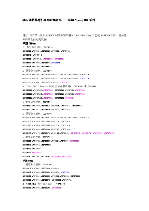
NEC/瑞萨单片机系列破解研究--早期Flash/ROM系列|目前,NEC第一代FLASH MCU制品分别采用0.35um和0.25um工艺或 MASKROM制作,目前能够得到全面完美破解:早期78K0s:1. 型号命名规则:78F90**uPD789022,uPD789024,uPD789025,uPD789026, uPD78F9026uPD789046, uPD78F9046uPD789052, uPD789062, uPD78E9860, uPD78E9861,uPD789071,uPD789072,uPD789074 uPD78F9076uPD789086,uPD789088 uPD78F90882. 型号命名规则:78F91**uPD789101,uPD789102,uPD789104,uPD789111,uPD789112,uPD789114, uPD78F9116uPD789121,uPD789122,uPD789124,uPD789131,uPD789132,uPD789134, uPD78F9136uPD789166,uPD789167,uPD789176,uPD789177 uPD78F91773. 78K0s/Kx1+ Lowpin 系列型号命名规则: 78F92** 或 78F95**uPD78F9200,uPD78F9201,uPD78F9202, uPD78F9500,uPD78F9501,uPD78F9502,uPD78F9210,uPD78F9211,uPD78F9212, uPD78F9510,uPD78F9511,uPD78F9512,uPD78F9221,uPD78F9222,uPD78F9224, uPD78F9232,uPD78F92344. 型号命名规则:78F93**uPD789304,uPD789306,uPD789314,uPD789316, uPD78F9314, uPD78F9316uPD789322,uPD789324,uPD789326,uPD789327, uPD78F93285. 型号命名规则:78F94**uPD789405,uPD789406,uPD789407,uPD789415,uPD789416,uPD789417, uPD78F9418uPD789425,uPD789426,uPD789435,uPD789436, uPD78F9436uPD789445,uPD789446,uPD789455,uPD789456, uPD78F9456uPD789462,uPD789464,uPD789466,uPD789467, uPD78F9468uPD789477,uPD789478,uPD789479,uPD789488,uPD789489, uPD78F9478,uPD78F9479, uPD78F9488,uPD78F9489,6. 型号命名规则:78F98**uPD789830,uPD789832,uPD789833,uPD789834,uPD789835 uPD78F9835uPD789841,uPD789842 uPD78F9842uPD789800 uPD78F9801uPD789881 uPD78F9882uPD789860,uPD789861,uPD789862 uPD78E9860A,uPD78E9861A早期78K0:1. 型号命名规则:78F00**uPD780021,uPD780022,uPD780023,uPD780024,uPD780031,uPD780032,uPD780033,uPD780034, uPD78F0034uPD780053,uPD780054,uPD780055,uPD780056,uPD780058, uPD78F0058uPD780065,uPD780076,uPD780078, uPD78F0066,uPD78F0078,2. 78K0/Kx1 型号命名规则: 78F01**uPD780101,uPD780102,uPD780103, uPD78F0103,uPD780111,uPD780112,uPD780113,uPD780114, uPD78F0114,uPD780131,uPD780132,uPD780133,uPD780134,uPD780136,uPD780138, uPD78F0134,uPD78F0138,uPD780143,uPD780144,uPD780146,uPD780148, uPD78F0148,3. 78K0/Kx1+ 型号命名规则:78F01**H 或 7801**HuPD780101H,uPD780102H,uPD780103H, uPD78F0103H,uPD780111H,uPD780112H,uPD780113H,uPD780114H, uPD78F0114H,uPD780131H,uPD780132H,uPD780133H,uPD780134H,uPD780136H,uPD780138H, uPD78F0134H,uPD78F0138H,uPD780143H,uPD780144H,uPD780146H,uPD780148H, uPD78F0148H,例: uPD780102H 为著名的SONY PSP游戏机电池加密芯片4. 型号命名规则: 78F02**uPD780232,uPD780233, uPD78F0233,5. 型号命名规则: 78F03**uPD780306,uPD780308, uPD78P0308,uPD780316,uPD780318,uPD780326, uPD780328,uPD780336, uPD780338, uPD78F0338,uPD780343,uPD780344,uPD780353, uPD780354, uPD78F0354,7. 型号命名规则: 78F07**uPD78F0714,8. 型号命名规则: 78F08**uPD780861,uPD780862, uPD78F0862A,uPD780822,uPD780824,uPD780826,uPD780828, uPD78F0822B,uPD78F0828A,9. 型号命名规则: 78F09**uPD780957 uPD78F0958uPD780982,uPD780983,uPD780984,uPD780986,uPD780988, uPD78F0988A10. ASSP 型号命名规则: 78F80**uPD788004,uPD788005,uPD788006, uPD78F8004,uPD78F8005,uPD78F8006,全部V850:1. V850/Sx1/2/3 型号命名规则:70F30**uPD703014,uPD703015,uPD703017, uPD70F3015,uPD70F3017,uPD703030,uPD703031,uPD703032,uPD703033 uPD70F3030,uPD70F3032,uPD70F3033uPD703034,uPD703035,uPD703036,uPD703037 uPD70F3035,uPD70F3036,uPD70F3037uPD703068,uPD703069,uPD703088,uPD703089, uPD70F3089uPD780065,uPD780076,uPD780078, uPD78F0066,uPD78F0078,早期V850ES:1. V850ES/Sx1/2 型号命名规则:70F32** 汽车仪表盘uPD703200,uPD703201,uPD703204, uPD70F3201,uPD70F3204,uPD703249,uPD703260,uPD703261,uPD703262,uPD703263, uPD70F3261,uPD70F3263uPD703264,uPD703265,uPD703266, uPD70F3264,uPD70F3265,uPD70F3266,uPD703252,uPD703270,uPD703271,uPD703272,uPD703273, uPD70F3271,uPD70F3273uPD703274,uPD703275,uPD703276, uPD70F3274,uPD70F3275,uPD70F3276,uPD703253,uPD703280,uPD703281,uPD703282,uPD703283, uPD70F3281,uPD70F3283uPD703284,uPD703285,uPD703286, uPD70F3284,uPD70F3285,uPD70F3286,2. V850ES/Fx2 型号命名规则: 70F32** 工业控制,汽车电子uPD703230,uPD703231,uPD703232,uPD703233,uPD703234,uPD703235uPD70F3231,uPD70F3232,uPD70F3233,uPD70F3234,uPD70F3235,uPD70F3236,uPD70F3237,uPD70F3238,uPD70F32393. V850ES/Ix 型号命名规则: 70F33** 70F37** 电机控制,空调变频器uPD703327,uPD703329, uPD70F3329uPD70F3713,uPD70F3714,4. V850ES/Kx1+ 型号命名规则: 70F33**uPD703302,uPD703313,uPD70F3302,uPD70F3306, uPD70F3308,uPD70F3311, uPD70F3313,uPD70F3316, uPD70F33185. V850ES/Hx2 型号命名规则: 70F37**uPD70F3700,uPD70F3701, uPD70F3702,uPD70F3703, uPD70F3704,uPD70F3706,uPD70F3707,uPD70F3710, uPD70F3711,uPD70F3712,6. V850ES/Jx2 型号命名规则: 70F37**uPD70F3715,uPD70F3716, uPD70F3717,uPD70F3718, uPD70F3719,uPD70F3720,uPD70F3721, uPD70F3722,uPD70F3723, uPD70F3724,7. V850ES/Kx2 型号命名规则: 70F37**uPD70F3726,uPD70F3728, uPD70F3729,uPD70F3731, uPD70F3732,uPD70F3733, uPD70F3734,8. V850ES/Sx3 型号命名规则: 70F33**uPD70F3333,uPD70F3334,uPD70F3335,uPD70F3336,uPD70F3340,uPD70F3341, uPD70F3342,uPD70F3343,uPD70F3344,uPD70F3345, uPD70F3346,uPD70F3347, uPD70F3348uPD70F3350,uPD70F3351, uPD70F3352,uPD70F3353, (奔驰C180~C260导航仪CAN协议IC)uPD70F3354,uPD70F3355, uPD70F3356,uPD70F3357, uPD70F3358uPD70F3364,uPD70F3365, uPD70F3366,uPD70F3367, uPD70F3368早期V850E1:1. V850E/Mx1/2/3 型号命名规则: 70F31**uPD703101,uPD703102, uPD70F3102uPD703105,uPD703106, uPD703107, uPD70F3107uPD703114,uPD703116, uPD703183,uPD703185,uPD703186, uPD70F3114,uPD70F3116, uPD70F3184,uPD70F3186,uPD703136,uPD703132, uPD703133,uPD703134, uPD70F31342. 安全气囊IC V850E/RS1 型号命名规则: 70F34**uPD70F3400,uPD70F3401上述型号解密周期为15~30天,企鹅是二六七一三六八七二四破解流程:客户提交母片 -> 破解进行 -> 破解完成,客户提交保证金(可使用支付宝) -> 当天提供2片测试样品寄给客户- >-> 客户测试OK -> 客户付尾款 -> 发BIN码给客户-> 客户测试NG -> 客户返还2片样品(需外观完好)-> 退还客户保证金NEC第二代全FLASH MCU制品分别采用0.25/0.15um(MF2)工艺制作,称为ALL FLASH品。
瑞萨_mcu型号指南

QzROM
PWM
16 8 DA
AD (LVD)
(POR)
/RTC PLL I/O
QzROM
群 型号
(4bits/W) RAM
(10bits/W) QzROM
存储器
)
(
最
/
高 工 最作 大频 范率 围工 作 电 压
最
小
指
令
执
端
行
口
时
间
时钟
电压 检测
SSOP-24
遥控器
7544
M37544G2ASP/GP M37544G2A-XXXSP/GP
8K
256
8MHz/ 1.8~5.5V
0.25us @8MHz
25 - - ○ ○ - - 10位×6
-
2 1 - - - ○ - - ○ ○ ○ - - 8 -20~85
SDIP-32 LQFP-32
OA设备、FA设备、家电、民用设备
M38588GCSP M38588GC-XXXSP
48K
1.5K
12.5MHz/ 2.4~5.5V
0.5us @8MHz
34 - ○ - - - - 8位×9
-
4 2 - - ○ ○ - - ○ ○ ○ - - 8 -20~85
SDIP-42 SSOP-42
OA设备、FA设备、家电、民用设备
M38D24G4FP/HP M38D24G4-XXXFP/HP
M34571G4FP M34571G4-XXXFP
M34571G6FP M34571G6-XXXFP
M34571GDFP M34571GD-XXXFP
WizPro200NX系列烧入器使用手册_Renesas_V1.0

WizPro200Nx(有数量控制功能) 编程器使用说明(For 瑞萨系列MCU)版本 1.01本烧写器支持的芯片:1.1Renesas Flash MCU R8C系列、M32C系列MCU,支持序列号功能。
序列号为4个字节长度,其在Flash中存放的地址可由用户通过PC应用程序随意设定,同时序列号的初始值和累加量也由用户自己随意设定;2特点:2.1支持瑞萨(Renesas) R8Cxx系列MCU,包括:R8Cxxx、M16Cxx、M32Cxx系列等;2.2支持UART编程接口;2.3支持3.3V和5.0V接口电平;2.4支持裸片烧写或在板烧写(In-Circuit-Program、On-Board-Program);2.5支持脱机烧写,烧写时无需连接电脑,方便生产线使用;2.6USB通讯接口,方便连接电脑的连接;2.7自动编程优化,编程速度快;2.8支持序列号的设定,地址任意选择;2.9支持烧写数量控制功能(针对方案开发公司该功能可以控制客户烧写的芯片数量,而保证方案公司的利益;2.10操作简单,单键触发,蜂鸣器和LED提示烧写的结果;2.11支持USB在线升级Firmware,便于器件的更新和扩展;2.12可整合成1拖n的烧写平台,满足大批量生产的需要;3外观接口图:4指示灯和蜂明器:2.1 电源指示灯:编程器接通电源后指示灯点亮,表示电源正常;2.2 状态指示灯(红色和蓝色LED灯):2.2.1:编程器通过USB连接到电脑时,打开编程器的PC软件时蓝色和红色的LED灯点亮,同时蜂鸣器响2次长声;2.2.2 编程器下载程序后接上电源时:¾红色和蓝色指示灯交替闪烁:表示系统正进行内部数据校验;¾红色灯亮同时蜂鸣器响2次长声:表示系统内部数据校验失败,须连接电脑重新下载 程序才可正常烧写;¾蓝色灯亮同时蜂鸣器响1次长声;表示系统内部数据校验成功,可以开始烧写芯片;¾蜂鸣器长响1声(约1秒钟):说明编程器内部的Firmware有问题,需到我司网站下载 最新的Firmware或联络我司(我司网址:)2.2.3 编程器完成校验后开始编程时:¾蓝色红色指示灯交替闪烁,表示编程器正在对目标芯片进行编程器;¾红色灯亮同时蜂鸣器响3次短声:表示对目标芯片编程器失败,请作相应检查;¾蓝色灯亮同时蜂鸣器响1次长声:表示对目标芯片编程成功;5按键和接口说明:5.1白色按键:编程器按键,按一下按键系统就开始对目标芯片编程;5.2电源接口:接9~12V DC Adapter,>300mA即可,随机配有一个DC电源适配器;5.3USB接口:用于进行下载程序或在线编程以及编程器内部数据的更新和设定;5.4编程接口:用于对MCU进行编程,排线中箭头指向的一端的为第一脚,注意排线的插入方向(有防呆设计)。
R5F100LEA瑞萨 MCU官方资料(2)

1. InstallationDo not connect the E1 debugger module until the software support has been installed.1.Insert the CD into your computer’s CD-ROM drive. The CD should automatically run the installation program.If the installer does not start, browse to the CD root folder and double click on ‘CsPlusLauncher.exe’.2.Windows™ Vista/Windows™ 7 users may see “User Account Control” dialog box. If applicable, enter theadministrator password and click <OK>.3.The pre installer will first check to see if the CubeSuite prerequisites are present, and will install if necessary(this may take a few minutes).4.Once the prerequisites are setup, the CubeSuite+ installer will launch.5.The CubeSuite+ Welcome window will appear. Click <Next>.6.The End User License Agreement appears. Read the license agreement and select <Accept> if you wish tocontinue. Click <Next>.7.The ‘Select Component’ window appears. Review the components by selecting each component in turn.Click <Next> to continue.8.The License Key Registration window appears. If you have a license key available, click the <LicenseManager> button, otherwise go to Step 9. Enter the license key in the opened ‘License Manager’ dialog. Add the license key. Click <Add>. If the license key is added successfully, click <Close>.9.Click <Next>.10.The ‘Installation Settings Confirmation’ window appears. Review the information and click <Next> to begininstallation.11.The ‘Installation Execution’ window will appear showing the install status progress. Before completion, theRenesas E-Series USB Driver installation dialog will appear. Windows™ Vista and Windows™ 7 users may see a ‘Windows Security’ dialog box. Click ‘Always trust software from “Renesas Solutions Corp.”’ then click <Install>. 12.After a successful installation click <Next>.13.The ‘Setup Completion’ window will appear. Click <Finish> to close the installer.2. Connection14.Fit the LCD module to the connector marked ‘LCD’ on the RSK. Ensure all the pins of the connector arecorrectly inserted in the socket.15.Connect the E1 debugger module to the connector marked ‘E1’ on the RSK using the ribbon cable.16.Connect the E1 debugger module to a spare USB port of your PC. The green ‘ACT’ LED on the E1 debuggerwill flash.17.The ‘Found New Hardware’ Wizard will appear. Please follow the steps below to install the drivers. Note that,administrator privileges are required for a Windows™ XP/Vista machine.Windows™ XP Windows™ Vista / Windows™ 7a.Select option ‘No, not this time’ in “Found NewHardware” Wizard dialog, and click <Next>button.a.“Device driver software installed successfully”pop-up will appear in the Windows toolbar andinstallation will complete.b.Verify the “Recommended” option is selectedand click <Next>.c.If using Windows™ XP, go to step ‘e’;otherwise, click <Next>.d.Click <Next> to install the driver.e.Click <Finish> to close the wizard.Note: The Windows driver signing dialog may be displayed. Please accept the driver to continue.18.The green ‘ACT’ LED on the E1 debugger will illuminate.3. CubeSuite+ ProjectCubeSuite+ integrates various tools such as compiler, assembler, debugger and editor into a common graphical user interface. To learn more on how to use CubeSuite+, refer to the CubeSuite+ Tutorial manual from the menu bar (Help > Tutorial).unch CubeSuite+ from the Windows Start Menu. (Start Menu > All Programs > Renesas ElectronicsCubeSuite+ > CubeSuite+).20.The ‘One Point Advice’ dialog which provides useful tips will open. The detail for this is out of scope for thisguide. Click <OK>.21.The Start panel will appear. Select the RSKRL78G13_Tutorial project under the “Open Sample RSK Project”and click <GO>.22.In the “Create Project” dialog that follows, specify a name for the project. Leave the list of subprojectsunselected.23.Click “Create” to launch the main Tutorial project.4. Programming and Debug24. Click on RL78 Simulator (Debug Tool) from the Project Tree pane and select the “RL78 E1 (Serial)” asshown in the following screenshot:25. Right-click on “RL78 E1(Serial) (Debug Tool)” and select ‘Property’.26. On the ‘Property’ tab, select “Power target from the emulator.(MAX200mA)”.27. Click on the drop-down menu button on the right and select “Yes”. A new entry, “Supply voltage”, will appear. 28.Click on the “Supply voltage” entry and change the voltage to 5.0V from the drop-down menu.29.Build the project by clicking on the Build Project button.30.Download the code to the microcontroller by clicking on the download buttonor click on Debug from the Menu bar and click on Download as shown below:31.Click the <Restart> button to reset the CPU then start program execution.The user LEDs on the board will flash at regular intervals. Pressing any of the switches on the RSK, or after 200 flashes have elapsed, will display the string STATIC on the second line of the debug LCD. The second line will then be replaced with the string TESTTEST one character at a time; whilst allowing you to control the user LEDs’ flashing rate using the potentiometer shaft. 32.Click the <Stop> button.The code will stop and the source code will be opened at the current program counter.5. Next StepAfter you have completed this quick start procedure, please review the tutorial code and sample code that came with the kit. You can review these codes by changing the active project to another project. The tutorials will help you understand the device and development process using Renesas Development Tools.The Hardware manual supplied with this RSK is current at the time of publication. Please check for any updates to the device manual from the Renesas internet site at: /rskrl78g136. Renesas RL78 CompilerThe version of the compiler provided with this RSK is fully functional with no time restrictions. The compiler will limit the code linker to 64k bytes. Full licensed RL78 compiler versions are available from your Renesas supplier.7. User ManualsUser manuals can found in the Windows Start Menu. (Start Menu > All Programs > Renesas ElectronicsCubeSuite+ > Readme Documents > RSK > RSKRL78G13).8. SupportOnline technical support and information is available at: /rskrl78g13 Technical Contact Details csc@Note on Update Manager : The Update Manager checks via Internet for any updated resources available for each installed CubeSuite+ tool and downloads them accordingly to simplify the update process. Automatic updates will not work if CubeSuite+ is installed without a license key.© 2011 Renesas Electronics Europe Limited. All rights reserved. © 2011 Renesas Electronics Corporation. All rights reserved. © 2011 Renesas Solutions Corp. All rights reserved. Website: D010234_11_S01_V01。
瑞萨汽车电子产品型号速查

封装
TO-263
TO-220
TO-262 HSON-8
5
TO-252
TO-220
TO-262
HSON-8
TO-252
TO-263
TO-263-7p
TO-263
TO-263-7p
TO-263
TO-262
TO-263-7p
TO-263
TO-263-7p
TO-263
TO-263
TO-263
TO-263
TO-263
2015.03
瑞
萨
电汽车电子用功率器件(Power MOSFET及IPD)
4
汽车电子用MCU-K系列(78K)
12
汽车电子用MCU-F系列(78K/RL78/V850/RH850)
14
汽车电子用MCU-D系列(RL78/78K)
26
汽车电子用MCU-SuperH族
28
汽车电子用MCU产品-RH850族
Rth(ch-C) (℃/W)
1.02 1.02 1.02 1.09 1.43 1.43 1.43 1.55
0.43 0.52 0.6 0.68 0.66 0.52 0.52 0.6 0.68 0.52 0.75 0.75 1.05 1.43 1.43 1.43 1.43 1.7 1.95 0.52 0.6 0.52 0.52
R8C族
AE1-L系 (ASSP)
开发工具与开发环境
芯片封装说明
Power MOSFET及IPD
K系列 (78K)
F系列 (78K/RL78/V850/RH850)
D系列 (RL78/78K)
SuperH族
RH850族
瑞萨MCU介绍_SH72531-r15

LiveDevices (Realogy)
Windriver (OSEKWorks)
CAN-Driver: Vector,Volcano,ETAS and Windriver
Compiler:
Renesas (HEW)
WindRiver (Diab C)
Greenhill (Greenhills C)
13
SH72531 Overview
Rev. 1.5
开发工具 瑞萨可提供配套开发工具
集成开发环境(IDE):HEW 编译器:SH C/C++ Toolchain 片上仿真器:E10A-USB 编程开发环境: FDT 下载器:E8A或通用UART电缆
14
SH72531 Overview
CPU频率
7
SH72531 Overview
Rev. 1.5
特色之一:领先的高速闪存技术 (2/2)
瑞萨拥有自主的FLASH技术,让您的设计如虎添翼!
结构形式
2005 2006 2007 2008 2009 2010 2011 2012 2013
结构
最高读取 速度
样品
量产
2014 2015
Floating Gate
RAM (KB)
300
SH-2A内核
256
SH72546R
SH72544R
128
SH72543R SH72531 SH72533
64
2
4
ROM (MB)
ATU-III
SH-2A Core 120MHz
DMAC A-DMAC
ROM Flash
RAM
IC 32bit x 4ch
瑞萨R5G0C51X中文资料
在开发中※本规格书为暂定规格书,今后还有可能更改。
R5G0C51群RCJ03B0035-0100 SINGLE-CHIP 8-BIT CMOS MICROCOMPUTER Rev.1.002006.09.29 概要R5G0C51群是采用了740族内核的8位单片机,是和38D2群管脚兼容的QzROM版,具有LCD驱动控制电路、A/D 转换器和串行接口等附加功能。
有多种不同的内部存储器容量和封装种类的产品。
有关详细内容请参照“产品型号、存储器容量和封装”。
特点●基本机器指令 (71)●指令执行时间 ...............................0.5μs(在最短指令、振荡频率为8MHz时)●存储器容量 ROM ........................................................................16K~60K字节RAM ........................................................................640~2048字节●可编程输入/输出端口 ..................................................51个(SEG共用24个)●中断 .........................................................................................15个源、13个向量●定时器 .......................................................................................8位×3、16位×2●串行接口 ......................................................................................................8位×1(UART或者时钟同步)●A/D转换器 ..................................................................................................8位×8●监视定时器....................................................................................................8位×1●LED直接驱动端口.............................................................................................8个(平均电流15mA、峰值电流30mA、总和电流90mA)●LCD驱动控制电路 偏压 ..............................................................1/2、1/3偏压分时 ..............................................................2、3、4分时公共输出 ......................................................................4个段输出 ........................................................................24个●主时钟发生电路 ..............................................................................内置1个电路(外接陶瓷谐振器或者晶体谐振器)●子时钟发生电路 ..............................................................................内置1个电路(外接晶体谐振器)●电源电压在2分频模式时(f(X IN)≤8MHz)....................................4.0~5.5V在2分频模式时(f(X IN)≤4MHz)....................................2.0~5.5V在4分频模式时(f(X IN)≤8MHz)....................................2.0~5.5V在8分频模式时(f(X IN)≤8MHz)....................................2.0~5.5V在低速模式时 ......................................................................2.0~5.5V●功耗在2分频模式时 ...............................................................标准21mW(Vcc=5V、f(X IN)=8MHz、Ta=25°C)在低速模式时 ...................................................................标准18μW(Vcc=2.5V、f(X IN)=停止、f(X CIN)=32kHz、Ta=25°C)●工作环境温度 .......................................................................................-20~85°C应用功率计和塔式空调等。
瑞萨芯片选型
SuperH RISC engine 族产品概要:SuperH是具有高性能价格比、小型化和高性能功耗比(MIPS/W)特性的嵌入式RISC单片机。
我们正在开发具有广泛的应用范围和多种功能的CPU内核,并提供有强大的产品阵容。
产品系列包含具有CPU内核、内部大容量快速擦写存储器和定时器、串行接口、AD转换器等外围功能的SH-2系列;具有能进行高速数据处理的CPU内核、高速缓冲存储器和MMU的SH-3系列或SH-4系列;具有全DSP功能和以多媒体处理/通信处理为主的CPU内核的SH2-DSP系列或SH3-DSP系列。
现在提供的产品还具有低功率模式、低功耗和小型化等许多特点。
改善了各种通用操作系统和开发工具,从而保证能实现更有效的开发。
主要应用•MPUo汽车导航系统、CIS、娱乐设备和多媒体设备。
o宽带路由器、防火墙、网络设备和因特网设备。
o小型打印机、直接打印机、POS终端、便携式终端和网络终端。
o DVC、DSC和图像处理设备等。
•MCUo空调、电冰箱和洗衣机。
o打印机、传真机和复印机。
o工业设备和机床。
o汽车引擎和动力转向系统。
.瑞萨MCU选型指南有想法吗?请使用我们的,为您寻找最合适的瑞萨产品。
Lineup:SH7780系列SH7780系列是搭载SH-4A CPU内核的高端SuperH处理器。
SH-4A的指令集是完全向上兼容的。
SH-4A的工作频率比已有的SH-4 CPU内核高的多。
并且SH-4A CPU内核具有支持单精度和双精度算术运算的FPU。
SH7722 | SH7723 | SH7724 | SH7730 | SH7731 | SH7763 | SH7764 | SH7780 | SH7781 | SH7785 | SH7786SH7450 系列SH7450系列高性能微控制器配有SH-4A CPU内核。
SH7450系列整合了大容量Flash存储器和SRAM,使其能够适用于汽车主动安全系统,如驱动支持。
瑞萨RDK-N9H20评估板用户手册说明书
ARM® ARM926EL-S Based32-bit MicroprocessorRDK-N9H20Demo Board User ManualThe information described in this document is the exclusive intellectual property of Nuvoton Technology Corporation and shall not be reproduced without permission from Nuvoton. Nuvoton is providing this document only for reference purposes of NuMicro microcontroller based system design. Nuvoton assumes no responsibility for errors or omissions.All data and specifications are subject to change without notice.For additional information or questions, please contact: Nuvoton Technology Corporation.Table of Contents1OVERVIEW (3)1.1Brief Introduction to RDK-N9H20 Demo Board (4)1.2PCB key parts description (4)1.3System Circuitry design notes (6)1.3.1Main Clock (6)1.3.2RTC Clock (6)1.3.3RESET (7)1.3.4Power-on Setting (7)1.3.5Power Desing Notes (8)2PCB Layout Design Note (10)2.1USB (10)2.2Signal integrity, SI (11)2.3Power supply and power filter design consideration (12)2.3.1DDR MVDD & Core Power 1.8V Design (12)2.3.2I/O 3.3V Power Design (13)2.4Main Clock 12MHz Design Suggestion (14)2.5RESET Layout Suggestion (15)3RDK-N9H20 demo board use description (16)3.1System start up (16)3.2USB Port (18)3.3Communication Interface (UART0) uses (18)3.4LCD Interface (18)4Test Report (19)Power consumption (19)4.14.2ESD Test Report (19)EFT Test Result (19)4.34.4EMI Test Result (20)5RDK-N9H20 demo board SCHEMATIC (22)5.1N9H20 Schematic (22)LCD Schematic (23)5.25.3Power Schematic (24)6REVISION HISTORY (25)1 OVERVIEWThe RDK-N9H20 is a general demo board installed the N9H20K51N chip which integrated 32MBDDR2 memory, users can verify emWin GUI application program easily.The demo board includes one Micro USB connector for USB 2.0 high speed device controller forcommunication with PC, and the board also has a debugging UART port for system programmingor debugging.About display, the RDK-N9H20 demo board included one 4.3”LCD which the resolution is480x272 with RGB-24bits and embedded the 4-wires resistive type touch panel.For system booting, the RDK-N9H20 demo board supports one SPI-NOR Flash or one NANDFlash for selection depended on user demand.NUTINY-SDK-NUC505 USER MANUALFigure 1-1 RDK-N9H20 demo boardBrief Introduction to RDK-N9H20 Demo Board1.1RDK-N9H20 demo board applied to HMI application, the purpose is for user have a reference design with emWin GUI accelerator platform. Thus that customers do not have to modify or only make simple changes could get a completed HMI hardware product quicklyThe following figures show the RDK-N9H20 demo board, in which the PCB integrated Nuvoton N9H20K51N 32-bit microcontroller with CPU core ARM926EJ-S, speed runs up at 192MHz, with 16KB I-cache, 16 KB D-cache and MMU, 8KB SRAM and 12KB IBR(Internal Boot ROM) for booting sources from USB ,SPI-NOR Flash or NAND Flash selectable.1.2PCB key parts descriptionThe PCB key parts are shown as the figureFigure 1-2 RDK-N9H20 PCB components sideNUTINY-SDK-NUC505 USER MANUALSystem Circuitry design notes1.31.3.1 Main ClockThe system clock circuit is formed by the feedback circuit inside the chip and the external 12MHzcrystal oscillation circuit. Recommended crystal connection mode and device parameters as shown in the figure below.Note: The chosen capacitance needs to match the load capacitance of the crystal oscillator1.3.2RTC ClockN9H20K51N integrates the RTC function, the board needs to provide the RTC with the clock circuit, the recommended Crystal connection mode and the device parameters as shown in the figure below.NUTINY-SDK-NUC505 USER MANUAL1.3.3 RESETThe nRST signal of the N9H20K51N is the reset signal input pin, and the required reset effective signal is a low-level pulse.In order to stabilize the system robustness, it is recommended to use the following circuitry to implement reset signal. The RDK-N9H20 demo board reset circuity and related passive device parameters as shown in the following figure.1.3.4 Power-on SettingThe power-on setting value is used to configure the chip to enter a specific state after power-up or reset. The power-on setting value will be kept in power-on setting control register for reference. The following is the RDK-N9H20 demo board power-on setting circuitry and functions description.1.3.4.1RDK-N9H20 demo board power-on setting description1.3.5 Power Desing NotesRDK-N9H20 demo board power supply design have the below considerations●For system core power (1.8V) design, it is recommended to select DC-DC part and the outputcapacity have 1A or above is better.●For IO power (3.3V), in RDK-N9H20 demo board also uses DC-DC part, the concern is for LCDpowered●Power up sequence, the I/O (3.3V) power should be equal or fast than the core (1.8V) powerand time gap between should control under within 500uS as the figure shown.●Power-down sequence, the Core (2.8V) power should be equal or fast than the I/O (3.3V) power.NUTINY-SDK-NUC505 USER MANUALNote. ● Yellow line is I/O (3.3V) ● Blue line is core (1.8V) ● Purple line is nRST signal2 PCB LAYOUT DESIGN NOTE.RDK-N9H20 demo board is a 2-layers PCB and single component side design, for getting good performance and system quality have some suggestions as the below please follow.USB2.1USB differential Line have 3 conditions as far as possible: 1, equal length; 2, equal width and 3, EquidistantTo do 90ohm ±10% impedance control. The double-layer plate can be controlled by the way of the impedance, that is, the differential line to do the GND shielding processing.The RDK-N9H20 demo board USB eys diagram result as the below fugureSignal integrity, SI2.2Due to 2- layers PCB does not have a separate GND plane, and to ensure the connectivity and integrity of the GND plane, the following requirements must be observed: ●The Bottom layer as far as possible or less device, to ensure the bottom surface of the GND integrity. Especially at the bottom of the main chip.,the RDK-N9H20 demo board that GND process at the bottom of main chip is shown in the following figure.● If that is possible please place more via holes to GND to ensure that the top surface and the bottom surface of the GND copper skin connectivity.● Ensure that there is no island of GND copper skin, as far as possible to ensure that as much as possible to connect the copper, so that the signal return path as short as possible.● High-speed signal line under the bottom surface, as far as possible to ensure the complete GND plane, do not have to walk through the line.●For critical signals, such as crystal oscillator, System Reset, I²C, USB, etc., need to be processed with shield GND all the way. The good shield GND process can guarantee the continuity of the impedance, anti-interference, and prevent EMI radiation.The following fugure is the LCD_CLK signle connectivity with shield GND processPower supply and power filter design consideration2.32.3.1 DDR MVDD & Core Power 1.8V DesignAbout filter capacitance material and placement quantityCapacity material recommended to use X7R material, placing quantity suggest that the corresponding chip should have at least one 104pF capacitors at the each supply pin, and some special entrances suggest placing the 104 pF+10 uF combination.Detail please refer to RDK-N9H20 schematic diagram for details.The layout pattern and the filter capacitance placement are shown in the image below.NUTINY-SDK-NUC505 USER MANUAL2.3.2 I/O 3.3V Power DesignAbout filter capacitance material and placement quantityCapacity material recommended to use X7R material, placing quantity suggest that the corresponding chip should have at least one 104pF capacitors at the each supply pin, and some special entrances suggest placing the 104 pF+10 uF combination.Detail please refer to RDK-N9H20 schematic diagram for details.The layout pattern and the filter capacitance placement are shown in the image below.2.4Main Clock 12MHz Design SuggestionThe 12MHz oscillator is the heart of the N9H20 chip and should be preferred in layout. Layout Basic principles: As close as possible to the chip pin, trace lines shoud be straight doesn’t be bent, and important thing is that XTAL part at the bottom has a complete GND plane.PCB layout skill was shown as below figure.NUTINY-SDK-NUC505 USER MANUALRESET Layout Suggestion2.5For system ESD capability and stability, the RESET signal design and layout traces routing are worth a comprehensive consideration to do that best protection.Schematic details please refer to the schematic diagram of the RDK-N9H20, about the PCB layout was shown as below figure.3 RDK-N9H20 DEMO BOARD USE DESCRIPTIONThe RDK-N9H20 demo board is powered by DC +5V and is accessed by the CON3 pin-1 (+5V) and the pin-4 (GND).The demo board system block as the figure.3.1System start upMode switching by Normal/USB recovery mode jumper (i.e. R64 install or not) as the be low figure ●R64 pin un-install: Normal operation for NAND or SPI FLASH booting●R64 pin installation: USB booting for code programming through writer tool of PC utility.NUTINY-SDK-NUC505 USER MANUAL3.2USB PortThe USB interface on the board is mainly used for burning the update program, this interface does not have the power supply capability. When using, please choose to connect with this interface USB extension cable connected with the PC and then power supply through the system supply port.CON33.3Communication Interface (UART0) usesCON3 interface is combined with UART0 serial port and +5V power supply, serial port level is standard TTL, communication baud rate is 115200bps.The development period can be used for debug, which can be used for data interaction after the product.3.4LCD InterfaceHMI-H9H20 demo board supports LCD interface with a 40-pin FPC connector, it is apply to 4.3” LCD resolution 480x272 RGB 24-bits and embedded 4-wires resistive type touch panel, the touch panel is connectivity with N9H20 ADC directly.4 TEST REPORT4.1Power consumptionCondition : CPU@192MHz , emWin demo code is running●Non-OS+emWin + 4.3 LCD:5V@335mA●Non-OS+emWin without LCD: 5V@98mA4.2ESD Test Report●Contact (PCB GND & LCD metal ):+/- 4KV pass●Air (LCD touch panel):+/- 8KV pass●Coupling (Horizontal & Vertical) :+/- 4KV passNUTINY-SDK-NUC505 USER MANUAL 4.3EFT Test Result●EFT±4000V 5.0KHz passEMI Test Result4.4EN55032 Test Result : PassNUTINY-SDK-NUC505 USER MANUALNUTINY-SDK-NUC505 USER MANUAL5 RDK-N9H20 DEMO BOARD SCHEMATIC 5.1N9H20 SchematicNUTINY-SDK-NUC505 USER MANUALLCD Schematic5.2Power Schematic 5.36 REVISION HISTORY2018.09.25 1.00 Initially issued.Important NoticeNuvoton Products are neither intended nor warranted for usage in systems or equipment, any malfunction or failure of which may cause loss of human life, bodily injury or severe property damage. Such applications are deemed, “Insecure Usage”.Insecure usage includes, but is not limited to: equipment for surgical implementation, atomic energy control instruments, airplane or spaceship instruments, the control or operation of dynamic, brake or safety systems designed for vehicular use, traffic signal instruments, all types of safety devices, and other applications intended to support or sustain life.All Insecure Usage shall be made at customer’s risk, and in the event that third parties lay claims to Nuvoton as a result of customer’s Insecure Us age, customer shall indemnify the damages and liabilities thus incurred by Nuvoton.。
瑞萨MCU型号速查手册
2010年4月1日 瑞萨电ቤተ መጻሕፍቲ ባይዱ公司
【发行】瑞萨电子公司() 【业务咨询】/inquiry
Notice
1. All information included in this document is current as of the date this document is issued. Such information, however, is subject to change without any prior notice. Before purchasing or using any Renesas Electronics products listed herein, please confirm the latest product information with a Renesas Electronics sales office. Also, please pay regular and careful attention to additional and different information to be disclosed by Renesas Electronics such as that disclosed through our website.