Agilent网络分析仪测试介绍
Agilent安捷伦阻抗网络分析仪-操作指导说明书
安捷伦精密阻抗网络分析仪-操作指导说明书
11 触发设置
[Trigger]键,根据需要设置,默认连续扫 描,即曲线实时更新状态; -SINGLE:单次扫描
12 测试记录
将器件安装至夹具,进行数据记录。
需要先按[Marker]键,再数字输入(或转 动旋钮选择)对应的信号值,进行所需 数据抓取。
安捷伦精密阻抗网络分析仪-操作指导说明书
4 选择功能
[Meas]键,根据所需测量的参数,进行测 试功能选择。
安捷伦精密阻抗网络分析仪-操作指导说明书
5 曲线形式设置 [Format]键,根据需要,选择线性/LIN 或 对数/LOG 的形式显示。
[Display]键,根据需要,选择不同的显示 功能: -SPLIT:对 A、B 曲线分开单独显示; -HIDE INACT:只显示选中的 A 或 B 曲线; 6 曲线显示设置 -ACCUMULATE: 对 测 试 的 曲 线 进 行 多 次 叠加显示; -OFFSET:可输入设置参数补偿
安捷伦精密阻抗网络分析仪-操作指导说明书
序号
步骤
操作内容
图示
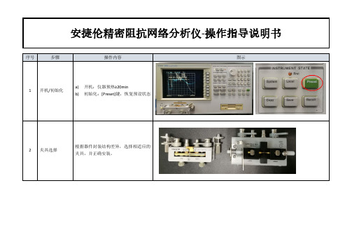
1 开机/初始化
a) 开机:仪器预热≥20min b) 初始化:[Preset]键,恢复预设状态
2 夹具选择
根据器件封装结构差异,选择相适应的 夹具,并正确安装。
安捷伦精密阻抗网络分析仪-操作指导说明书
[Cal]键,选择 FIXTURE COMPEN,进行以 下操作: 3 校准/减少误差 a) OPEN:开路清“0” b) SHORT:短路清“0”(需放置短路片)
13 结束
关机
安捷伦精密阻抗网络分析仪-操作指导说明书
9 信号源输入
[Start]键,再用数字键输入相应的起始信 号值; [Stop]键,再用数字键输入相应的终止信 号值;
Agilent 8714ET网络分析仪操作指导书06
2.为了再次观察两个测量通道,按MEASE1。
为了在分开的屏幕上同时观察两个测量通道,按DISPLAY,More Display,Split Disp FULL split。
1.用分析仪自带的电缆连接到分析仪的Port1和Port2端口。
2.按PRESET,SCALE,0.1 Enter
1.按POWER,0,dBm。
2.按CAL,Default Respone。
3.检验数据示迹应落在0dB±0.5dB的范围内。
1.用分析仪自带的电缆连接到分析仪的Port1和Port2端口。
2.按MEAS1,More Power,FREQ,Start 10,MHz,SCALE,1,Enter。
Reference Level软按键,可以读取当前传输值;
为了在分开的屏幕上同时观察两个测量通道,按DISPLAY,More Display,Split Disp FULL split。
按面板上的Format键,可选择改变参考方式:
1)LOG MAG(对数幅度)
选择此键可以进行传输测量(比如增益、插入损耗);
2.设置频率高端,按Stop,再按数字键和单位键,键入设定值。或用Center和Span软件来设置频率范围。
3.按面板的Marker,设置需要标记的频点,共设置8个;
4.按POWER键,显示屏出现电平菜单,按Level,再按数字键和单位键,键入功率电平设定值Level=10dBm(在PORT2连接50dB高功率衰减器的情况下);
项目
操作步骤
操作方法
操作要求
备注事项
1.射频网络分析仪第一次通电前的检查
2.上电,预热
Agilent_8753D网络分析仪操作指导书
1.按面板上的[MENU]键、按屏幕上的软按键[POWER],再按数字键和单位键[x1],键入设定值。通常下POWER Level设为10 dBm,
2.按面板上的[CAL]键、依次按屏幕上的软按键[CALIBRATEMENU]、[S111-PORT]
3.电源线必须使用带有保护地线的三芯电源线。电源插头座必须是带有保护地线的三芯电源插头座。确保仪器设备接地良好,不会造成人身伤害。
1.按电源POWER键。当电源开关接通时,电源指示灯LED(绿灯)亮。
2.在进行测量之前,让射频网络分析仪预热5分钟。
这组测量键为每一测量通道选择测量。分析仪的测量能力包括传输、反射、功率、变频损耗和多端口选择等。
这组信号源键可选择所希望送到被测件上的源输出信号。这组信号源键还控制扫描时间、点数及扫描触发。
这组配置键控制接收机和显示器的参数,包括接收机带宽和平均,显示刻度和格式、标记功能以及仪器校准等。
电源电压选择开关应在230V电压档位
电源保险丝应为5A250V
电源插头,插座必须是带有保护地线的三芯插头座,
按面板上的Marker键,按屏幕上的软按键1~4,分别输入数值及单位,设置频率标记。
按面板上的Format键,可选择改变参考方式:
1)LOG MAG(对数幅度)
2)PHASE(相位)
3)SWR(驻波比)
4)DELAY(延时)
5)SMITH(史密斯圆图)
6)POLAR(极坐标)
7)LIN MAG(线性幅度)
最大输入电平:+10dBm
损坏电平:±26dBm或35Vdc
阻抗:50Ω(用选件075时为75Ω)
使用 Agilent E5061B 低频-射频网络分析仪测量频率响应
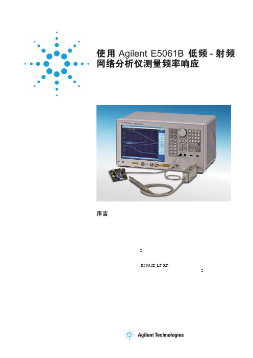
使用 Agilent E5061B 低频-射频网络分析仪测量频率响应应用指南序言测量元器件和电路的频率响应特性是确保电子设备性能的关键步骤。
汽车、医疗设备、航空航天与国防行业对电子设备的可靠性要求极高,因此在从低频至高频的各种频率范围内对各类元器件和电路进行测量非常必要。
在这些应用中,低频网络分析仪在确保低频模拟电路器件(例如传感器系统和电源部件)实现稳定可靠工作方面具有重要作用。
为此,您需要在了解射频网络分析(S 参数测量)的同时,也需要很好地对低频网络分析(增益相位测量)的应用有所了解。
本应用指南通过对 E5061B LF-RF 网络分析仪的介绍,阐述了有关低频网络分析的基础原理。
我们在此主要介绍简单的低频 2 端口器件测量,以及高阻抗探测技术和大衰减测量等相关主题。
目录E5061B-3L5 LF-RF 网络分析仪 (3)基本测量配置 (4)50 Ω被测器件 (5)非 50 Ω被测器件,实例 1 (5)非 50 Ω被测器件,实例 2 (7)使用探头在电路板上直接进行测量 (8)低频测量的 IFBW 设置 (10)使用高阻抗探头的测量方法 (11)做比值测量时对信号的分离 (13)在低频范围内测量大衰减器件 (15)运算放大器测量实例 (20)闭环增益 (20)开环增益,相位裕量 (22)CMRR (27)PSRR (29)输出阻抗 (31)参考文献 (33)表 1.测试端口选择指南23E5061B-3L5 LF-RF 网络分析仪包含选件 3L5 的 E5061B 矢量网络分析仪具有很宽的频率测量范围,从 5 Hz 至 3 GHz 。
E5061B-3L5 包括 S 参数测试端口(5 Hz 至 3 GHz ,Z in = 50 Ω)和增益相位测试端口(5 Hz 至 30 MHz ,Z in = 1 M Ω/50 Ω)。
两种测试端口都可以用于低频器件的测试(取决于测量需求)。
表 1 举例说明了怎样选择使用这两种测试端口。
网络分析仪使用手册

1 2
4
二.注意事项
1 在测试设备前面始终有一个导电的工作台垫 2 在进行清洁、检查或连接到对静电敏感的器件或测试端 口之前,您自己始终应接地 3 在连接到分析仪测试端口或其它对静电敏感的器件上之 前,始终应将测试电缆的内导体接地 4 在进行器件连结时,请利用利用扭力扳手完成最终连接,进行 紧固,直到达到扭力扳手,不要冲过起始停止点,可以利用辅 助扳手防止连接器主体旋转
图9
第 9 頁,共 18頁
審核 :
吳健誌
製表:王彦武
仪 器 作 業 說 明
一. 操作說明
网络分析仪(Agilent E5071B) ENA 网络分析仪操作步骤<4-2>
版 本
0
2 设置测试状态
a. 配置最大通道数和迹线数 System Setup Press: Misc Setup Return Channel/Trace
5 4 图7 3
第 7 頁,共 18頁
審核 :
吳健誌
製表:王彦武
仪 器 作 業 說 明
一. 操作說明
1 2 3 4 5 6 7 8 9 Handler I/O 接口 并行接口 串行接口 键盘/鼠标接口 LAN/USB 接口 GPIB 接口 VGA 输出 内部参考输出 内部参考输入
网络分析仪(Agilent E5071B) ENA 网络分析仪接口<3-1>
Vinc
Vref=? 图3
第 3 頁,共 18頁
審核 :
吳健誌
製表:王彦武
仪 器 作 業 說 明
网络分析仪(Agilent E5071B) ENA 网络分析仪测试基础知识<1-4>
版 本
0
一. 操作說明 1 S 参数 S 参数是用入射波和反射波和描述网络特性 如图4所示 Reflected S11= Incident Transmitted S21= incident Reflected S22= Incident Transmitted S12= Incident 二.注意事项
ilentEC网络分析仪测试方法

i l e n t E C网络分析仪测试方法集团标准化办公室:[VV986T-J682P28-JP266L8-68PNN]Agilent E5071C网络分析仪测试方法-李S买卖仪器没找到联系方式请搜索《欧诺谊-李海凤》进入查看联系方式,谢谢!E5071C网络分析仪测试方法一.面板上常使用按键功能大概介绍如下:Meas 打开后显示有:S11 S21 S12 S22 (S11 S22为反射,S21 S12 为传输)注意:驻波比和回波损耗在反射功能测试,也就是说在S11或者S22里面测试。
Format 打开后显示有:Log Mag———SWR———-里面有很多测试功能,如上这两种是我们常用到的,Log Mag为回波损耗测试,SWR 为驻波比测试。
Display打开后显示有:Num of Traces (此功能可以打开多条测试线进行同时测试多项指标,每一条测试线可以跟据自己的需求选择相对应的指标,也就是说一个产品我们可以同时测试驻波比和插入损耗或者更多的指标)Allocate Traces (打开此功能里面有窗口显示选择,我们可以跟据自己的需求选择两个窗口以上的显示方式)Cal 此功能为仪器校准功能:我们常用到的是打开后在显示选择:Calibrate (校准端口选择,我们可以选择单端口校准,也可以选择双端口校准)Trace Prev 此功能为测试线的更换设置Scale 此功能为测试放大的功能,打开后常用到的有:Scale/Div10DB/Div 为每格测试10DB,我们可以跟据自己的产品更改每格测量的大小,方便我们看测试结果Reference Value 这项功能可以改变测试线的高低,也是方便我们测试时能清楚的看到产品测试出来的波型。
Save/Recall 此功能为保存功能,我们可以把产品设置好的测试结果保存在这个里面进去以后按下此菜单Save State 我们可以保存到自己想保存的地方,如:保存在仪器里面请按 Recall State 里面会有相对应的01到08,我们也可以按SaveTrace Data 保存在外接的U盘里面,方便的把我们产品的测试结果给客户看。
Agilent 4395A 网络 频谱 阻抗分析仪数据手册说明书
Network Measurement1.At relative to 0 dBm output, 50 MHz,23 °C ±5 °C /HP-Agilent-4395A-Spectrum-Network-Analyzer.aspx To buy, sell, rent or trade-in this product please click on the link below:2Network MeasurementcontinuedReceiver CharacteristicsInput characteristicsFrequency range . . . . . . . . . . . . . . . . . . . . . . . . . . . . . . . . . . . . . . . . . . .10 Hz to 500 MHzInput attenuator . . . . . . . . . . . . . . . . . . . . . . . . . . . . . . . . . . . . . . . . .0 to 50 dB, 10 dB stepFull scale input level (R, A, B)Attenuator setting (dB) Full scale input level0–10 dBm100 dBm20+10 dBm30+20 dBm40+30 dBm50+30 dBmIF bandwidth (IFBW)2, 10, 30, 100, 300, 1 k, 3 k, 10 k, 30 kHzNote: The IFBW should be set to less than 1/5 of the lowest frequency inthe sweep range.Noise level (referenced to full scale input level, 23 °C ±5 °C)at 10 Hz ≤frequency < 100 Hz, IFBW = 2 Hz . . . . . . . . . . . . . . . . . . . . . .–85 dB (SPC)at 100 Hz ≤frequency < 100 kHz, IFBW = 10 Hz . . . . . . . . . . . . . . . . . . . . . . . . .–85 dBat 100 kHz ≤frequency, IFBW = 10 Hz . . . . . . . . . . . . . . . . . . . . . . . . . . . . . .-–115 dBInput crosstalkfor input R + 10 dBm input, input attenuator: . . . . . . . . . . . . . . . . . . . . . . . . . . . . .20 dBfor input A, B input attenuator: . . . . . . . . . . . . . . . . . . . . . . . . . . . . . . . . . . . . . . . . .0 dBat < 100 kHzR through A, B . . . . . . . . . . . . . . . . . . . . . . . . . . . . . . . . . . . . . . . . . . . . . .< –100 dBothers . . . . . . . . . . . . . . . . . . . . . . . . . . . . . . . . . . . . . . . . . . . . . . .< –100 dB (SPC)at ≥100 kHzR through A, B . . . . . . . . . . . . . . . . . . . . . . . . . . . . . . . . . . . . . . . . . . . . .< –120 dBothers . . . . . . . . . . . . . . . . . . . . . . . . . . . . . . . . . . . . . . . . . . . . . . .< –120 dB (SPC)Source crosstalk (for input A, B)(typical for input R)at + 10 dBm output, < 100 kHz, input attenuator: 0 dB . . . . . . . . . . . . . . . . .< –100 dBat + 10 dBm output, ≥100 kHz, input attenuator: 0 dB . . . . . . . . . . . . . . . . .< –120 dBMultiplexer switching impedance changeat input attenuator 0 dB . . . . . . . . . . . . . . . . . . . . . . . . . . . . . . . . . . . . . . . .< 0.5% (SPC)at input attenuator 10 dB and above . . . . . . . . . . . . . . . . . . . . . . . . . . . . . .< 0.1% (SPC)Connector . . . . . . . . . . . . . . . . . . . . . . . . . . . . . . . . . . . . . . . . . . . . . . . . . . . .Type-N femaleImpedance . . . . . . . . . . . . . . . . . . . . . . . . . . . . . . . . . . . . . . . . . . . . . . . . . . . .50 ΩnominalReturn lossInput attenuator0 dB10 dB20 dB to 50 dB10 Hz ≤frequency < 100 kHz25 dB125 dB125 dB1100 kHz ≤frequency ≤100 MHz25 dB125 dB25 dB1100 MHz < frequency15 dB115 dB15 dB1Maximum input level+30 dBm (at input attenuator: 40 dB or 50 dB)Maximum safe input level+30 dBm or ±7 Vdc (SPC)1.SPC34Absolute amplitude accuracy (R, A, B)at –10 dBm input, input attenuator:10 dB, frequency ≥100 Hz, IFBW ≤3 kHz, 23 °C ±5 °C, . . . . . . . . . . . .< ±1.5 dB Ratio accuracy (A/R, B/R) (typical for A/B)at –10 dBm input, input attenuator:10 dB, IFBW ≤3 kHz, 23 °C ±5 °C, . . . . . . . . . . . . . . . . . . . . . . . . . . . . . . .< ±2 dB Dynamic accuracy (A/R, B/R) (typical for A/B)Input level Dynamic accuracy 1(relative to full scale input level)frequency ≥100 Hz 0 dB ≥input level > –10 dB ±0.4 dB –10 dB ≥input Level ≥–60 dB ±0.05 dB –60 dB > input level ≥–80 dB ±0.3 dB –80 dB > input level ≥–100 dB ±3 dB Figure 1-1. Magnitude dynamic accuracy Residual responses . . . . . . . . . . . . . . . . . . . . . . . . . . . . . . . . . . .< –80 dB full scale (SPC)Trace noise (A/R, B/R, A/B)at 50 MHz, both inputs: full scale input level –10 dB, IFBW = 300 Hz . . . . . . . . . . . . . .< 0.005 dB rms (SPC)Stability (A/R, B/R, A/B) . . . . . . . . . . . . . . . . . . . . . . . . . . . . . . . .< ±0.01 dB/°C (SPC)Phase characteristics Measurements format . . . . . . . . . . . . . . . . . . .Standard format, expanded phase format Frequency response (deviation from linear phase) (A/R, B/R) (SPC for A/B) at –10 dBm input, input attenuator: 10 dB, IFBW ≤3 kHz, 23 °C ±5 °C . . . . . .< ±12°Dynamic accuracy (A/R, B/R) (SPC for A/B)Input level Dynamic accuracy 1(relative to full scale input level)frequency ≥100 Hz 0 dB ≥input level > –10 dB ±3°–10 dB ≥input Level ≥–60 dB ±0.3°–60 dB > input level ≥–80 dB ±1.8°–80 dB > input level ≥–100 dB ±18°Magnitude Characteristics1.R input level (B input level for A/B) = fullscale input level –10 dB, IFBW = 10 Hz,23 °C ± 5 °CInput level (dB)Magnitude dynamic accuracy D y n a m i c a c c u r a c y (d B )Spec Typical5Figure 1-2. Phase dynamic accuracyTrace noise (A/R, B/R, A/B)at 50 MHz, both inputs:full scale input level –10 dB, IFBW = 300 Hz . . . . . . . . . . . . . . . . .< 0.04°rms (SPC)Stability (A/R, B/R, A/B) . . . . . . . . . . . . . . . . . . . . . . . . . . . . . . . . . . .< ±0.1 °/°C (SPC)Group delay characteristicsAperture [Hz] . . . . . . . . . . . . . . . . . . . . . . . . . . . . . . . . . . . . . . . . . . .0.25% to 20% of span AccuracyIn general, the following formula can be used to determine the accuracy, in seconds,of a specific group delay measurement: . . . . . . . . . . . .Phase accuracy (degree)Aperture(Hz) x 360 (degree)Sweep characteristicsSweep type . . . . . . . . . . . . . . . . .Linear frequency, log frequency, power, list frequency Sweep direction . . . . . . . . . . . . . . . . . . . . . . . . . . . . . . . . . . . . . . . . . .Upper direction only Trigger type . . . . . . . . . . . . . . . . . . . . . . . . . .Hold, single, number of groups, continuous Trigger source . . . . . . . . . . . . . . . . . . . .Internal (free run), external, manual, GPIB (bus)Event trigger . . . . . . . . . . . . . . . . . . . . . . . . . . . . . . . . . . . . . . . . . . . . . .On point, on sweepInput level (dB)Phase dynamic accuracyD y n a m i c a c c u r a c y (d e g r e e )Spec Typical6Frequency characteristics Frequency range . . . . . . . . . . . . . . . . . . . . . . . . . . . . . . . . . . . . . . . . . . .10 Hz to 500 MHz Frequency readout accuracy . . . . . . . .±((freq readout [Hz ]) x (freq ref accuracy [1]) + RBW [Hz ] + SPAN [Hz ])) [Hz ]where NOP means number of display points NOP -1Frequency reference (Option 4395A-800)Accuracy at 23 °C ±5 °C, referenced to 23 °C . . . . . . . . . . . . . . . . . . . . . . . . . . . . .< ±5.5 ppm Aging . . . . . . . . . . . . . . . . . . . . . . . . . . . . . . . . . . . . . . . . . . . . .< ±2.5 ppm/year (SPC) Initial achievable accuracy . . . . . . . . . . . . . . . . . . . . . . . . . . . . . . . .< ±1.0 ppm (SPC) Temperature stability at 23 °C ±5 °C, referenced to 23 °C . . . . . . . . . . . . . . . . . . . . . . . . .< ±2 ppm (SPC) Precision frequency reference (Option 4395A-1D5) Accuracy at 0 °C to 40 °C, referenced to 23 °C . . . . . . . . . . . . . . . . . . . . . . . . . . .< ±0.13 ppm Aging . . . . . . . . . . . . . . . . . . . . . . . . . . . . . . . . . . . . . . . . . . . . . . . . .< ±0.l ppm/year (SPC)Initial achievable accuracy . . . . . . . . . . . . . . . . . . . . . . . . . . . . . . . . .< ±0.02 ppm (SPC)Temperature stability at 0 °C to 40 °C, referenced to 23 °C . . . . . . . . . . . . . . . . . . . . . . . .< ±0.01 ppm (SPC)Resolution bandwidth (RBW)Range 3 dB RBW at span > 0 . . . . . . . . . . . . . . . . . . . . . . . . . . . . . .1 Hz to 1 MHz, 1-3 step 3 dB RBW at span = 0 . . . . . . . . . . . .3 k, 5 k, 10 k, 20 k, 40 k, 100 k, 200 k, 400 k, 800 k, 1.5 M, 3 M, 5 MHz Selectivity (60 dB BW/3 dB BW)at span > 0 . . . . . . . . . . . . . . . . . . . . . . . . . . . . . . . . . . . . . . . . . . . . . . . . . . . . . . . .< 3Mode . . . . . . . . . . . . . . . . . . . . . . . . . . . . . . . . . . . . . . . . . . . . . . . . . . . . .Auto or manual Accuracy at span > 0 . . . . . . . . . . . . . . . . . . . . . . . . . . . . . . . . . . . . . . . . . . . . . . . . . . . .< ±10%at span = 0 . . . . . . . . . . . . . . . . . . . . . . . . . . . . . . . . . . . . . . . . . . . . . . . . . . . .< ±30%Video bandwidth (VBW)Range at span > 0 . . . . . . . . . . . . . . . .3 MHz to 3 MHz, 1-3 step, 0.003 ≤VBW/RBW ≤1Noise sidebands Offset from carrier Noise sidebands ≥1 kHz < –95 dBc/Hz ≥100 kHz < –108 dBc/Hz Figure 1-3. Noise sidebandsSpectrum Measurement Frequency offset [Hz]N o i s e s i d e b a n d [d B c /H z ]Spec Typical7Amplitude range . . . . . . . . . . . . . . . . . . . . . . . . . .displayed average noise level to +30 dBm Reference value setting range . . . . . . . . . . . . . . . . . . . . . . . . . . . . . .–100 dBm to +30 dBm Level accuracy at –20 dBm input, 50 MHz, input attenuator: 10 dB, 23 °C ±5 °C . . . . . . . . . . .< ±0.8 dB Frequency response at -20 dBm input, input attenuator: 10 dB, referenced to level at 50 MHz, 23 °C ±5 °C frequency ≥100 Hz . . . . . . . . . . . . . . . . . . . . . . . . . . . . . . . . . . . . . . . . . . . . . .< ±1.5 dB frequency < 100 Hz . . . . . . . . . . . . . . . . . . . . . . . . . . . . . . . . . . . . . . . . . . . . . .< ±1.3 dB Amplitude fidelity 1Log scale 2Range Amplitude fidelity (dB to reference input lever [dB][dB]0 to –30±0.05–30 to –40±0.07–40 to –50±0.15–50 to –60±0.35–60 to –70±0.8–70 to –80±1.8Linear scale 2 . . . . . . . . . . . . . . . . . . . . . . . . . . . . . . . . . . . . . . . . . . . . . . . . . . . . . . . . . . .< ±3%Displayed average noise level at reference value ≤–40 dBm, input attenuator: auto or 0 dB at frequency ≥1 kHz . . . . . . . . . . . . . . . . . . . . . . . . . . . . . . . . . . . . . . . . . . . .–120 dBm/Hz at ≥100 kHz . . . . . . . . . . . . . . . . . . . . . . . . . . . . . . . . . . . . . . . . . . . . . . . . . . .–133 dBm/Hz at ≥10 MHz . . . . . . . . . . . . . . . . . . . . . . . . . . . . .(–145 + frequency/100 MHz) dBm/Hz 3Figure 1-4. Typical displayed average noise level Amplitude Characteristics1.Fidelity shows an extent of nonlinearity referenced to the reference input level.2.RBW = 10 Hz, –20 dBm ≤reference value ≤+30 dBm, reference input level = full scale input level –10 dB, 23 ±5 °C3. At start frequency ≥10 MHzNote: Refer to Input attenuator part for the definition of full scale input level.Frequency offset [Hz]A v e r a g e n o i s e l e v e l [d B m /H z ]SpecTypical8Figure 1-5. Typical on-screen dynamic range (center: 100 MHz)Spurious responses Second harmonic distortion at single tone input with full scale input level –10 dB, input signal frequency ≥100 kHz . . . . . . . . . . . . . . . . . . . . . . . . . . . . . . . . . . . . . . . . . . .< –70 dBc, < –75 dBc (SPC)Third order inter-modulation distortion at two tones input with full scale input level –16 dB, separation ≥100 kHz . . . . . . . . . . . . . . . . . . . . . . . . . . . . . . . . . . . . . . . . . . . .< –75 dBc, < 80 dBc (SPC)Spurious at single tone input with full scale input level –10 dB, input signal frequency ≤500 MHz . . . . . . . . . . . . . . . . . . . . . . . . . . . . . . . . . . . . . . . . . . . . . . . . . . . . . . . . . .< –75 dBc except for the following frequency ranges:5.6 MHz ±1 MHz, 30.6 MHz ±1 MHz, 415.3 MHz ±1 MHz Residual response at reference value setting ≤–40 dBm, input attenuator: auto or 0 dB . . . . .< –110 dBmOn-screen Dynamic Range Offset frequency [Hz]O n -s c r e e n d y n a m i c r a n g e [d B c ]9Figure 1-6. Typical dynamic range at inputs R, A, and B Input attenuator Setting range . . . . . . . . . . . . . . . . . . . . . . . . . . . . . . . . . . . . . . . .0 dB to 50 dB, 10 dB step Attenuator setting (dB) Full scale input level 0–20 dBm 10–10 dBm 200 dBm 30+10 dBm 40+20 dBm 50+30 dBm Mode . . . . . . . . . . . . . . . . . . . . . . . . . . . . . . . . . . . . . . . . . . . . . . . . . . . . . . . . .Auto or manual (In auto mode, the attenuator is set to 20 dB above the reference value; this ensures that the maximum signal level after the attenuator will not be greater than –20 dBm.)Input attenuator switching uncertainty at attenuator: ≤30 dB, referenced to 10 dB . . . . . . . . . . . . . . . . . . . . . . . . . . . . .< ±1.0 dB at attenuator: ≥40 dB, referenced to 10 dB . . . . . . . . . . . . . . . . . . . . . . . . . . . .< ±1.5 dB Temperature drift . . . . . . . . . . . . . . . . . . . . . . . . . . . . . . . . . . . . . . . . . .< ±0.05 dB/°C (SPC)Scale Log 0.1 dB/div to 20 dB/div Linear at watt . . . . . . . . . . . . . . . . . . . . . . . . . . . . . . . . . . . . . . . . . . . . . . . . . . .1.0 x 10-12W/div at volt . . . . . . . . . . . . . . . . . . . . . . . . . . . . . . . . . . . . . . . . . . . . . . . . . . . . .1.0 x 10-9V/div Measurement format . . . . . . . . . . . . . . . . . . . . . . . . . . . . . . . . . . . . .Spectrum or noise (/Hz) Display unit . . . . . . . . . . . . . . . . . . . . . . . . . . . .dBm (unit of marker: dBm, dBV, dBµV, V, W)Sweep characteristics Sweep type . . . . . . . . . . . . . . . . . . . . . . . . . . . . . . . . . . . . . . . . . . . . . . . . . . . . . .Linear, list Trigger type . . . . . . . . . . . . . . . . . . . . . . . . . . .Hold, single, number of groups, continuous Trigger source . .Internal (free run), external, manual, level gate, edge gate, GPIB (bus)Sweep time (excluding each sweep setup time)RBW SPAN Typical sweep time 1 MHz 500 MHz 190 ms 100 kHz 100 MHz 300 ms 10 kHz 10 MHz 240 ms 1 kHz 1 MHz 190 ms 100 Hz 100 kHz 270 ms 10 Hz 10 kHz 2.0 s 1 Hz 1 kHz 11 s—Zero Span —1Typical Dynamic Range1.See the next item for sweep time at zero span Input level (dB)(Relative to full scale input level)D y n a m i c r a n g e (d B )Sensitivity (1 Hz RBW)Sensitivity ( 100 Hz RBW)2nd harmonic distortion 3rd order inter-modulation distortion Second Third1011Gate lengthRange . . . . . . . . . . . . . . . . . . . . . . . . . . . . . . . . . . . . . . . . . . . . . . . . . . . . . . .6 µs to 3.2 s ResolutionRange of gate length (T I )Resolution 6 µs ≤T I ≤25 ms 0.4 µs 25 ms < T I ≤64 ms 1 µs 64 ms < T I ≤130 ms 2 µs 130 ms < T I ≤320 ms 5 µs 320 ms < T I ≤1.28 s 20 µs 1.28s < T I ≤3.2 s100 µsGate lengthRange . . . . . . . . . . . . . . . . . . . . . . . . . . . . . . . . . . . . . . . . . . . . . . . . . . . . . . .2 µs to 3.2 sResolutionRange of gate delay (T d )Resolution 2 µs ≤T d ≤25 ms 0.4 µs 25 ms < T d ≤64 ms 1 µs 64 ms <T d ≤130 ms 2 µs 130 ms < T d ≤320 ms 5 µs 320 ms < T d ≤1.28 s 20 µs 1.28 s < T d ≤3.2 s100 µsAdditional amplitude errorLog scale . . . . . . . . . . . . . . . . . . . . . . . . . . . . . . . . . . . . . . . . . . . . . . . . . .< 0.3 dB (SPC)Linear scale . . . . . . . . . . . . . . . . . . . . . . . . . . . . . . . . . . . . . . . . . . . . . . . . . .< 3% (SPC)Gate control modes . . . . . . . . . . . . . . . . . . . . . . . . . . . . .Edge (positive/negative) or level Gate trigger input (external trigger input is used)Connector . . . . . . . . . . . . . . . . . . . . . . . . . . . . . . . . . . . . . . . . . . . . . . . . . . . .BNC female Level . . . . . . . . . . . . . . . . . . . . . . . . . . . . . . . . . . . . . . . . . . . . . . . . . . . . . . . . . . . . . . .TTL Gate outputConnector . . . . . . . . . . . . . . . . . . . . . . . . . . . . . . . . . . . . . . . . . . . . . . . . . . . .BNC female Level . . . . . . . . . . . . . . . . . . . . . . . . . . . . . . . . . . . . . . . . . . . . . . . . . . . . . . . . . . . . . . . .TTLSpecifications when Option 4395A-1D6 Time-Gated Spectrum Analysis is InstalledAll specifications are identical to the standard Agilent 4395A except the following items.12Measurement functions Measurement parameters Z, Y, L, C, Q, R, X, G, B, θDisplay parameters IZI, 0z , R, X, IYI, θy , G, B, I ΓI, θγ, Γx , Γy , Cp, Cs,Lp, Ls, Rp, Rs, D, QDisplay formats•Vertical lin/log scale •Complex plane•Polar/Smith/admittance chart Sweep parameters•Linear frequency sweep•Logarithmic frequency sweep •List frequency sweep•Power sweep (in dBm unit)IF bandwidth•2,10, 30, 100, 300, 1k, 3k, 10k, 30k [Hz]Calibration•OPEN/SHORT/LOAD 3 term calibration •Fixture compensation •Port extension correction Measurement port type •7-mm Output characteristicsFrequency range . . . . . . . . . . . . . . . . . . . . . . . . . . . . . . . . . . . . . . . . . .100 kHz to 500 MHz Frequency resolution . . . . . . . . . . . . . . . . . . . . . . . . . . . . . . . . . . . . . . . . . . . . . . . . .1 MHz Output impedance . . . . . . . . . . . . . . . . . . . . . . . . . . . . . . . . . . . . . . . . . . . . .50 Ωnominal Output levelwhen the measurement port is terminated by 50 Ω1 . . . . . . . . . . . . . .–56 to +9 dBm when the measurement port is open . . . . . . . . . . . . . . . . . . .0.71 mVrms to 1.26 Vrms Resolution . . . . . . . . . . . . . . . . . . . . . . . . . . . . . . . . . . . . . . . . . . . . . . . . . . . . . . . . . . .0.1 dBm Level accuracy . . . . . . . . . . . . . . . . . . . . . . . . . . . . . . . . . . . .±(A + B + 6 x F/(1.8 x 109))dB WhereA = 2 dBB = 0 dB (at 0 dBm ≤P ≤+ 15 dBm) or B = 1 dB (at –40 dBm ≤P < 0 dBm) or B = 2 dB (at –50 dBm ≤P < –40 dBm)F is setting frequency [Hz], P is output power settingOption 4395A-010Impedance measurementThe following specifications are applied when the 43961A impedance test kit is connected to the 4395A.1.When the measurement port is terminated with 50 Ω, the signal level at the measure-ment port is 6 dB lower than the signal level at the RF OUT port.13Measurement accuracy is specified at the connecting surface of the 7-mm connector of the Agilent 43961A under the following conditions:Warm up time . . . . . . . . . . . . . . . . . . . . . . . . . . . . . . . . . . . . . . . . . . . . . . . . .> 30 minutes Ambient temperature . . . . . . . . . . . . . . . . . . . . . . . . . . . . . . . . . . . . . . . . . . . .23 °C ±5 °C,within ±1 °C from the temperature at which calibration is performedSignal level (setting) . . . . . . . . . . . . . . . . . . . . . . . . . . . . . . . . . . . . . . . . . . .0 to +15 dBm Correction . . . . . . . . . . . . . . . . . . . . . . . . . . . . . . . . . . . . . . . . . . . . . . . . . . . . . . . . . . . . .ON IFBW (for calibration and measurement) . . . . . . . . . . . . . . . . . . . . . . . . . . . . . .≤300 Hz Averaging factor (for calibration and measurement) . . . . . . . . . . . . . . . . . . . . . . . . .≥8Figure 1-7. Impedance measurement accuracyIZI - θaccuracy IZI accuracy Z a = A + (B /I Z m I + C x I Z m I) x 100 [%]θaccuracy θa = sin -1(Z a /100)Where, I Z m I is I Z I measured. A, B, and C are obtained from Figure 1-7.IYI - θaccuracy IYI accuracy Y a = A + (B x I Y m I + C /I Z m I) x 100 [%]θaccuracy θa = sin -1(Y a /100)Where, I Y m I is I Y I measured. A, B, and C are obtained from Figure 1-7.Measurement Basic Accuracy(Supplemental performancecharacteristics)Test frequency [Hz]14Display LCDSize/type . . . . . . . . . . . . . . . . . . . . . . . . . . . . . . . . . . . . . . . . . . . . . . .8.4 inch color LCD Number of pixels . . . . . . . . . . . . . . . . . . . . . . . . . . . . . . . . . . . . . . . . . . . . . . . .640 x 480Effective display area . . . . . . . . . . . . . . . . . . . . . . .160 mm x 115 mm(600 x 430 dots)Number of display channels . . . . . . . . . . . . . . . . . . . . . . . . . . . . . . . . . . . . . . . . . . . . .2Format single, dual (split or overwrite)Number of traces . . . . . . . . . . . . . . . . . . . . . . . . . . . . . . . . . . . . . . . . . . . . . . . . . . . . . . . . . .For measurement . . . . . . . . . . . . . . . . . . . . . . . . . . . . . . . . . . . . . . . . . . . . . . . . .2 traces For memory . . . . . . . . . . . . . . . . . . . . . . . . . . . . . . . . . . . . . . . . . . . . . . . . . . . . . .2 traces Data math . . . . . . . . . . . . . . . . . . . . . . . . . . . . . . . . . . . . . . . . . . . . . . .gain x data – offset,gain x (data - memory) – offset,gain x (data + memory) – offset,gain x (data/memory ) – offsetData hold . . . . . . . . . . . . . . . . . . . . . . . . . . . . . . . . . . . . . . .Maximum hold, minimum hold MarkerNumber of markersMain marker . . . . . . . . . . . . . . . . . . . . . . . . . . . . . . . . . . . . . . . . . . . .l for each channel Sub-marker . . . . . . . . . . . . . . . . . . . . . . . . . . . . . . . . . . . . . . . . . . . . .7 for each channel ∆marker . . . . . . . . . . . . . . . . . . . . . . . . . . . . . . . . . . . . . . . . . . . . . . .1 for each channel Hard copyMode . . . . . . . . . . . . . . . . . . . . . . . . . . . .Dump mode only (including color dump mode)StorageBuilt-in flexible disk driveType . . . . . . . . . . . . . . . . . . . . . . . . . . . . . . . . . . . . . .3.5 inch, 1.44 MByte, or 720 KByte,1.44 MByte format is used for disk initializationMemory . . . . . . . . . . . . . . . . . . . . . . . . . . .512 KByte, can be backed up by flash memory GPIBInterface . . . . . . . . . . . . . . . . . . . . . . . . . . . . . . . . . . . . .IEEE 488.1-1987, IEEE 488.2-1987,IEC 625, and JIS C 1901-1987 standards compatible.Interface function . . . . . . . . . . . . . . . . . . . . . . . . .SH1, AH1, T6, TEO, L4, LEO, SR1, RL1,PP0, DC1, DT1, C1, C2, C3, C4, C11, E2Data transfer formats . . . . . . . . . . . . . . . . . . . . . . . . . . . . . . . . . . . . . . . . . . . . . . . . .ASCII,32 and 64 bit IEEE 754 floating point format,DOS PC format (32 bit IEEE with byte order reversed)Printer parallel portInterface . . . . . . . . . . . . . . . . . . . . . . . . . . . . . . .IEEE 1284 Centronics standard compliant Printer control language . . . . . . . . . . . . . . . . . . . . . . . . . . .PCL3 printer control language Connector . . . . . . . . . . . . . . . . . . . . . . . . . . . . . . . . . . . . . . . . . . . . . . . . . . .D-SUB (25-pin)15Common toNetwork/Spectrum/Impedance Measurement16Option 4395A-001 DC voltage/current sourceThe setting of Option 4395A-001 DC voltage/current source is independent of channel 1 and channel 2 settings.VoltageRange . . . . . . . . . . . . . . . . . . . . . . . . . . . . . . . . . . . . . . . . . . . . . . . . . . . . .–40 V to +40 V Resolution . . . . . . . . . . . . . . . . . . . . . . . . . . . . . . . . . . . . . . . . . . . . . . . . . . . . . . . . .1 mV Current limitationat voltage setting = –25 V to +25 V . . . . . . . . . . . . . . . . . . . . . . . . . . . . . .±100 mAat voltage setting = –40 V to –25 V, 25 V to 40 V . . . . . . . . . . . . . . . . . . .±20 mA CurrentRange–20 µA to -100 mA, 20 µA to 100 mAResolution . . . . . . . . . . . . . . . . . . . . . . . . . . . . . . . . . . . . . . . . . . . . . . . . . . . . . . . . . . .20 µA Voltage limitationat current setting = –20 mA to +20 mA . . . . . . . . . . . . . . . . . . . . . . . . . . . . . . .±40 V at current setting = –100 mA to –20 mA, 20 mA to 100 mA . . . . . . . . . . . . . .±25 V AccuracyVoltageat 23 °C ±5 °C . . . . . . . . . . . . . . . . . . . . . . .±(0.1% + 4 mV + I dc1[mA] x 5 [Ω] mV) Currentat 23 °C ±5 °C . . . . . . . . . . . . . . . . . . . . . . .±(0.5% + 30 µA + V dc2[V]/10 [kΩ] mA) Probe powerOutput voltage . . . . . . . . . . . . . . . . .+15 V (300 mA), –12.6 V (160 mA), GND nominal Specifications when instrument BASIC is operatedKeyboard . . . . . . . . . . . . . . . . . . . . . . . . . . . . . . . . . . . . .PS/2 style 101 English keyboard Connector . . . . . . . . . . . . . . . . . . . . . . . . . . . . . . . . . . . . . . . . . . . . . . . . . . . . . .mini-DIN 8 bit I/0 portConnector . . . . . . . . . . . . . . . . . . . . . . . . . . . . . . . . . . . . . . . . . . . . . . . . .D-SUB (15-pin) Level . . . . . . . . . . . . . . . . . . . . . . . . . . . . . . . . . . . . . . . . . . . . . . . . . . . . . . . . . . . . . . .TTL Number of input/output bit . . . . . . . . . . . . . . . . . . . . . .4 bit for input, 8 bit for outputFigure 1-8. 8 bit I/O port pin assignments24-bit I/O interfaceConnector . . . . . . . . . . . . . . . . . . . . . . . . . . . . . . . . . . . . . . . . . . . . . . . . . . .D-SUB (36-pin) Level . . . . . . . . . . . . . . . . . . . . . . . . . . . . . . . . . . . . . . . . . . . . . . . . . . . . . . . . . . . . . . . . .TTL I/O . . . . . . . . . . . . . . . . . . . . . . . . . . . . . . . . . . .8-bit for input or output, 16-bit for output Figure 1-9. 24-bit I/O interface pin assignment1.Current at DC source connector.2.Voltage at DC source connector.Table 1-1. Signal source assignmentPin No. Signal name Signal standard1GND0 V2INPUT1TTL level, pulse input (pulse width: 1 µs or above) 3OUTPUT1TTL level, latch output4OUTPUT2TTL level, latch output5OUTPUT PORT A0TTL level, latch output6OUTPUT PORT A1TTL level, latch output7OUTPUT PORT A2TTL level, latch output8OUTPUT PORT A3TTL level, latch output9OUTPUT PORT A4TTL level, latch output10OUTPUT PORT A5TTL level, latch output11OUTPUT PORT A6TTL level, latch output12OUTPUT PORT A7TTL level, latch output13OUTPUT PORT B0TTL level, latch output14OUTPUT PORT B1TTL level, latch output15OUTPUT PORT B2TTL level, latch output16OUTPUT PORT B3TTL level, latch output17OUTPUT PORT B4TTL level, latch output18OUTPUT PORT B5TTL level, latch output19OUTPUT PORT B6TTL level, latch output20OUTPUT PORT B7TTL level, latch output21I/O PORT C0TTL level, latch output22I/O PORT C1TTL level, latch output23I/O PORT C2TTL level, latch output24I/O PORT C3TTL level, latch output25I/O PORT D0TTL level, latch output26I/O PORT D1TTL level, latch output27I/O PORT D2TTL level, latch output28I/O PORT D3TTL level, latch output29PORT C STATUS TTL level, input mode: LOW, output mode: HIGH 30PORT D STATUS TTL level, input mode: LOW, output mode: HIGH 31WRITE STROBE SIGNAL TTL level, active low, pulse output(width: 10 µs; typical)32+5 V PULLUP33SWEEP END SIGNAL TTL level, active low, pulse output(width: 20 µs; typical)34+5 V+5 V, 100 mA MAX35PASS/FAIL SIGNAL TTL level, PASS: HIGH, FAIL: LOW, latch output36PASS/FAIL WRITE STROBE SIGNALTTL level, active low, pulse output(width: 10 µs; typical)1718Input and output characteristicsExternal reference inputFrequency . . . . . . . . . . . . . . . . . . . . . . . . . . . . . . . . . . . . . . . . . .10 MHz ±100 Hz (SPC)Level . . . . . . . . . . . . . . . . . . . . . . . . . . . . . . . . . . . . . . . . . . . . .-5 dBm to +5 dBm (SPC)Input impedance . . . . . . . . . . . . . . . . . . . . . . . . . . . . . . . . . . . . . . . . . . . . .50 Ωnominal Connector . . . . . . . . . . . . . . . . . . . . . . . . . . . . . . . . . . . . . . . . . . . . . . . . . . . .BNC female Internal reference outputFrequency . . . . . . . . . . . . . . . . . . . . . . . . . . . . . . . . . . . . . . . . . . . . . . . .10 MHz nominal Level . . . . . . . . . . . . . . . . . . . . . . . . . . . . . . . . . . . . . . . . . . . . . . . . . . . . . . .0 dBm (SPC)Output impedance . . . . . . . . . . . . . . . . . . . . . . . . . . . . . . . . . . . . . . . . . . .50 Ωnominal Connector . . . . . . . . . . . . . . . . . . . . . . . . . . . . . . . . . . . . . . . . . . . . . . . . . . . .BNC female Reference oven output (Option 4395A-1D5)Frequency . . . . . . . . . . . . . . . . . . . . . . . . . . . . . . . . . . . . . . . . . . . . . . . .10 MHz nominal Level . . . . . . . . . . . . . . . . . . . . . . . . . . . . . . . . . . . . . . . . . . . . . . . . . . . . . . .0 dBm (SPC)Output impedance . . . . . . . . . . . . . . . . . . . . . . . . . . . . . . . . . . . . . . . . . . .50 Ωnominal Connector . . . . . . . . . . . . . . . . . . . . . . . . . . . . . . . . . . . . . . . . . . . . . . . . . . . .BNC female External trigger inputLevel . . . . . . . . . . . . . . . . . . . . . . . . . . . . . . . . . . . . . . . . . . . . . . . . . . . . . . . . . . . . . . .TTL Pulse width (Tp) . . . . . . . . . . . . . . . . . . . . . . . . . . . . . . . . . . . . . . . . . . .≥2 µs typically Polarity . . . . . . . . . . . . . . . . . . . . . . . . . . . . . . . . . . . . . . . . .positive/negative selective Connector . . . . . . . . . . . . . . . . . . . . . . . . . . . . . . . . . . . . . . . . . . . . . . . . . . . .BNC female External program Run/Cont inputConnector . . . . . . . . . . . . . . . . . . . . . . . . . . . . . . . . . . . . . . . . . . . . . . . . . . . .BNC female Level . . . . . . . . . . . . . . . . . . . . . . . . . . . . . . . . . . . . . . . . . . . . . . . . . . . . . . . . . . . . . . .TTL Gate output (Option 4395A-1D6)Level . . . . . . . . . . . . . . . . . . . . . . . . . . . . . . . . . . . . . . . . . . . . . . . . . . . . . . . . . . . . . . .TTL Connector . . . . . . . . . . . . . . . . . . . . . . . . . . . . . . . . . . . . . . . . . . . . . . . . . . . .BNC femaleFigure 1-10. Trigger signal (external trigger input)General CharacteristicsPositive trigger signalNegative trigger signal。
AgilentE5062A网络分析仪导电性测试通用作业指导
AgilentE5062A网络分析仪导电性测试通用作业指导一.目的:规定使用AgilentE5062A网络分析仪测试VM件导电性的作业程序.二.校准和初始化设置:在测量开始前需要对网络分析仪进行校准,并且建立一个测量的基准。
如果没有量测夹具的基准,以下程序也就无法执行,校准程序如下:按下“启动/关机”按纽,启动仪器;并点击程序图标进入。
2.按下“Reset”键清除之前设定的内容3.按下“Start”,输入1600MHz. 4.按下“Stop”,输入2100MHz.5.按下“CAL”进入校准菜单6.点击“CALKIT”键,选择“85033E”7.点击“CALIBRATE”选择“1-PORTCal”8.用数据线将端口1和校准工具连接起来(数据线须用胶带固定),装上“OPEN”,并点击相应菜单9.装上“SHORT”,并点击相应菜单10.最后再装上“LOAD”,并点击相应菜单,然后点击“DONE”键11.可以点击“SAVE/RECALL”和“SAVESTATE”,保存此校准过程,同样以后可以点击“SAVE/RECALL”键来调出此校准过程12.按下“MEAS”键,再点击“S11”13.按下“FORMAT”,再点击“LOGMAG”14.用数据线将端口1和校准工具连接起来(数据线和夹具均须固定)15.按下“Scale”键,选择“Scalediv”,输入“5×1”16.按下“DISPLAY”键,注意不可有其他物品太靠近夹具,避免受到外部因素干扰17.点击“DATA(MEMORY”键18.选择“DATAANDMEMORY”键使记忆曲线和目前现实的曲线一同显现出来。
此时,你如果用手靠近夹具的话从屏幕上可以看到波形的偏移。
三.上下限设定选择“Marker”键,点击“Marker1”,转动旋钮使指针位于波形的波谷处,然后选择“Marker→RefMarker”将此设定为参考值选择“Marker2”输入“-50MHz”选择“Marker3”,输入“50MHz”将“RefMarkerMode”设为“OFF”记下Marker1、2、3所对应的频率值。
AgilentEA射频网络分析仪使用
仪器仪表的技术性能及指标假定带宽为 10Hz, 用 85032F 校准箱校准,运转环境温度为 23℃±5℃,与校准温度差值 <1℃且丈量数据不取均匀。
系统阻抗: 50Ω;频次范围: 300KHz~1.5GHz;最大功率: 10dBm;最小功率 ( 不加衰减器 ) :-45dBm(-5dBm);系统动向范围 ( 不加衰减器 ) :115dB(300kHz~1MHz) ,120dB(1MHz~3GHz)扫描种类:线性,幂,对数,分段波道数: 4每波道轨迹数: 4显示器: 10.4 英寸彩色 LCD显示器操作规范使用者要爱惜仪器,保证文明使用。
1)开机前保证稳压电源及仪器地线的正确连结。
2)使用中不得接触仪器接头内芯(含连结电缆)3)使用时不一样意工作台有较大振动。
4)使用中不可以任意切断电源,造成不正常关机。
不可以屡次开关机。
5)使用射频电缆时不要使劲大,保证电缆保持较大的弧度。
用毕电缆接头上加接头盖。
6)旋接接头时,要旋接头的螺套,尽量保证内芯不旋转。
7)尽量协调、少用校准件。
校准件用毕一定加盖放回器件盒。
8)转接件用毕应加盖后放回盒中。
9)停用时一定关机,封闭稳压电源,方可打扫卫生。
7、使用细则一、按左下方的电源键启动矢量网络剖析仪,启动后,待仪器达成自检后进入启动界面。
初始状态的默认值以下:开端频次 ----300KHz停止频次 ----1.5GHz端口输出功率 ----0dBm丈量点数 ----201 个轨迹代表的丈量值 ----S21显示格式 ----dBMAG参照电平 ----0dB参照线地点 ----第 8 格二、开端状态设置:1功率电平设定㈠按“ POWER/BW/AVG ”键,进入“功率 /丈量带宽 /均匀值设置”菜单㈡按“ POWER”键-数字键-单位键达成功率电平设定。
如:“POWER”键-0-X1,即设定功率电平为 0dBm。
,“-”为随后之意。
注意功率设定不得高出仪器提示范围(本仪器的范围是 -45dBm 到+10dBm),不然无效。
Agilent N9320B频谱分析仪介绍
图 2-2参考信号在屏幕外的 Delta标记对
使用 Delta 标记比较不在同一屏幕上的信号
使用
delta
标记功能对不在同一屏幕上的两个信号之间的频率和幅度差异进行测量
。(此功能适合于测量谐波失真)
此例中,使用频谱仪的
等都是前面板上的硬键。多数情况下,按下这样一个硬键将进入一个功能菜单,此菜单显
示在屏幕的右边上,如复位类型,中心频率和下一个峰值等。而这些显示在屏幕上的键被
称为软键。
使用前面板
这一节将介绍如何使用分析仪的基本功能。
输入数据
当需要输入参数值时,有以下几种常用的数据输入编辑方式:
旋纽
增加或减少当前值。
箭头按键
上的橙色指示灯亮起。
7 电源接口 用作频谱仪的电源输入端口。
8 VGA 端口 此视频输出端口可连接到一个外部显示器或投影仪。
9 USB端口 当您需要程控此频谱仪时,此端口用于连接电脑。
2 功能与应用
2.1 基本测量
在本介绍中,标有 [
] 的键,比如 [Preset/System], [Frequency]以及 [Marker]
提供了可选购的 AM/FM调制分析功能。
• 跟踪信号发生器
提供了可选购的射频跟踪信号发生器,用于进行标量网络分析。
• 分辨率为 0.1Hz 的频率计数器
频谱分析仪内置的计数器可使信号的频率测量精度达到 0.1Hz。
• 支持 USB 功率传感器
内置的功率计功能支持安捷伦
U2000
系列功率传感器,满足高精度功率测量的需求。
增加或减少当前值。
数字键
- 1、下载文档前请自行甄别文档内容的完整性,平台不提供额外的编辑、内容补充、找答案等附加服务。
- 2、"仅部分预览"的文档,不可在线预览部分如存在完整性等问题,可反馈申请退款(可完整预览的文档不适用该条件!)。
- 3、如文档侵犯您的权益,请联系客服反馈,我们会尽快为您处理(人工客服工作时间:9:00-18:30)。
方向性 低插入损耗
Detector
Test Port
定向耦合器连接端点: 反射特性测试点
定向耦合器用于器件反射性能测试
(入射信号泄漏) (被测件反射方向)
(定向耦合器输入端)
Directivity 方向性
反映定向耦合器 分离两个相反传输 方向信号的能力.
定向耦合器
反射方向
0 DUT RL = 40 dB Device
反射损耗 = -20 log(),
=
驻波比
Voltage Standing Wave Ratio
Emin
传输信号包络
Emax VSWR = Emin
=
1+
1-
全匹配 (ZL = Zo)
全反射
dB
1
0
RL VSWR
(ZL = 开路,短路 )
1 0 dB
page 6
史密斯圆图 (Smith Chart) 对阻抗和反射的描述
输入
R
反射
输出
B
A
反射特性
Reflected Incident = A R
传输特性
Transmitted = B R
Incident
SWR S参数 S11,S22 反射系数
反射损耗
增益 S参数 S21,S12 相位 Phase
群延时 Delay 传输系数 T,
page 15
,
阻抗 R+jX, G+jB
Mag(PMout) Mag(AMin)
(deg/dB)
PM (deg)
Mag(PM out)
I
Output Response
Time
AM to PM conversion can cause bit errors
page 20
网络分析仪
网络分析仪测试基本概念
网络分析仪 工作原理
误差和校准 ENA PNA
Data = Vector Sum
接收机类型
SOURCE
Incident
Transmitted
DUT
Reflected
Diode
Scalar broadband (no phase information)
DC
SIGNAL SEPARATION
REFLECTED (A) TRANSMITTED (B)
被测件端口 输入方向
Direc tivity Dev ice
被测件反射信号 与定向耦合器泄漏的 输入信号 在接收机端矢量叠加 影响测试精度
Return Loss
3 0 6 0 Frequency
Directivity
Device
Data Min Cancel Data 0
Directivity
Data Max Add in Phase
小电阻区
大电阻区
Z L = 0 (短路点)
ZL =
(开路点) O =1 0
= 1
±180
O
电容区
Z=R+jx
page 7
反射特性的说明
RS RL / RS RL
对于复阻抗: 功率最大传输效率条件:
ZL = ZS* (共轭匹配)
1.2
Load Power (normalized)
1 0.8 0.6 0.4 0.2 0 0 1 2 3 4 5 6 7 8 9 10
0.1
0.01
0.001 0 -5 -10 -15 -20 -25 -30 -35 -40 -45 -50 -55 -60 -65 -70
Interfering signal (dB)
T/R vs S-Parameter Test Sets
Transmission/Reflection Test Set
R 输入参考信号
A
N*LO +/- IF
B
输出信号
反射
传输
RF
输入信号
A R :被测件输入端反射特性
B R :被测件正向传输特性
信号源
提供被测件激励信号 具备频率和功率扫描功能 合成源实现
源功率控制
ALC
频率合成源
源功率控制部分= ALC: 小范围功率调整,功率扫描 + 衰减器: 大范围功率调整
-100dB
接收机噪声电平小,网络 分析测试动态范围大
接收机噪声电平高,网络 分析测试动态范围小
网络分析仪测试动态范围和测试精度
网络分析仪测试精度与测试动态范围关系
Error Due to Interfering Signal
100
10
+
phase error
Error (dB, deg)
1
magn error
高灵敏度接收机 ENA 采用混频方式接收机 接收机噪声电平与其接收带宽有关 网络分析仪要求大测试动态范围 对被测件输出杂波/谐波有抑制作用 接收机带宽在测试动态范围和测试速度间 折衷
混频器前端
ADC / DSP
幅度+相位信息
300kHz
8.5 GHz
网络分析仪的测试动态范围
接收机带宽:10Hz
接收机带宽 :70kHz
平衡/非平衡转换
page 3
射频信号在器件中的传播
入射 透射
反射
Lightwave
RF/MW
page 4
网络分析仪测试要讨论的问题
器件性能的描述: 传输特性; 反射特性 器件传输特性/反射特性的指标定义 ? Gain, Phase, Group delay VSWR, , , Impedance
Frequency
w
tg
群时延抖动
Dw
Phase
D
aperture
to 平均时延
Group Delay (tg) =
-d dw
Frequency
=
-1 360 o
*
d df
w
in radians
in radians/sec in degrees
网络分析仪通过测试相/频特性得 到器件延迟性能
INCIDENT (R)
RECEIVER / DETECTOR
PROCESSOR / DISPLAY
RF
AC
Tuned Receiver
RF IF = F LO ±F RF
ADC / DSP
IF Filter
Vector (magnitude and phase)
LO
调谐接收机的特点
Time
Time
输入信号
输出信号
Frequency
Frequency
page 17
器件的功率动态范围:
CH1 S21 C2 1og MAG 1 dB/ REF 32 dB 30.991 dB 12.3 dBm
输入1dB压缩点
1 dB compression point: 输入功率增加导致器件增益下降1dB 相对测试 输出1dB压缩点(绝对测试)
Frequency
Phase
Frequency
幅度/频率特性要求
相位/频率特性要求
page 11
对系统相位特性的描述
网络分析仪的相位补偿处理功能:
• 电延迟功能( Electrical delay):通过时间补偿消除被测件相频特性中线性部分 • 相位偏移(Phase offset): 被测件相位特性中加入固定偏置 • 端口延伸(Port Extension):测试仪表端口电延时补偿
page 21
网络分析仪组成框图
源 功率分配/开关
R1
参考接收机 衰减器
参考接收机 衰减器
网络分析仪组成
R2
A
B
•信号源 •信号分离装置 •接收机 •处理显示单元
测量接收机
Port 1
反射信号 (A) DUT
传输分析仪测试信号流程
输入源 LO 源
器件相频特性
Phase 45 /Div
o
网络分析仪相位补偿 (Electrical delay )
器件相位非线性
= Phase 1 /Div
o
+
Frequency Frequency
Frequency
测量器件相位特性 难于定量分析相位特性线性
应用:
便于对相位特性线性的分析
应用:
page 12
群时延Group Delay (GD)
源 衰减器
Range1 Range2 Range3 ….
ALC Driver
端口稳定点频输出:
span=0Hz, max sweep time
ALC = 自动电平控制 (automatic level control)
ALC 检测
信号分离装置
50 W 6 dB
功分器
提供参考信号 宽频率覆盖
Incident Transmitted
Zs = R + jX
R L / RS
ZL = Zs* = R - jX
RL = RS: 负载上最大功率传输
page 8
传输特性
V
输入
V
DUT
传输
传输系数 =
T
=
VTransmitted
VIncident
V V
Trans Inc
=
插入损耗 (dB) = - 20 Log
= - 20 log
S参数的定义