数字电路 讲义 353f13sept20-slides-3x3
合集下载
数字电路 完整课件讲解

• 栅极电容的电荷不易泄漏掉,容易由于外界静电 感应积累电荷,在栅极产生较高的电压,造成栅极 氧化层击穿,损坏MOS管。
2.1.4 MOS 管的开关特性
• 在数字集成电路中,一般都 在输入端加上保护电路。如图 在GS间加保护二极管DZ,当静 电压超过一定限度后,二极管 击穿导通,使静电荷泄放保护 氧化层不被击穿。
二、 CMOS 与非门、或非门、与门和或门
2、CMOS门电路的构图原则
①工作管(NMOS)与负载管(PMOS)要成对出现。 同一对NMOS、PMOS管栅极接在一起作为输入端; NMOS管的B极均接地,PMOS管的B极均接电源 ②工作管相串,相应的负载管应相并;工作管相并 相应的负载管相串。 ③工作管先串后并,则负载管应先并后串,工作管 先并后串,则负载管先串后并。 ④工作管相串为“与”,相并为“或”,由工作 管组 与负载管组联接点引出则倒相。
二个概念:
(1)输出高电平电流IOH
• 输出uo为高电平时,CMOS反相 器中,PMOS管T2导通,NMOS管T1 截止。Io从VDD经TP流出,供给负 载 RL 。 • 这时负载RL是向反相器索取电流,所以常常形 象地称之为拉电流负载,并把反相器能够输出的 最大电流IOH,叫带拉电流负载的能力。
(二)CMOS反相器的静态特性 2、输出特性: uo f (i0 )
(二)CMOS反相器的静态特性 1、输入特性: i I f (u I )
• 正常工作电压情况下,由于MOS 管输入电阻很高,iI≈0;
• 当uI>VDD+uDF时,保护二极管
D3导通,电流急剧增加; 当uI< - uDF时,D1导通,i1经D1、
RS流出,见P96图2.3.3(c)
(二)CMOS反相器的静态特性 2、输出特性: uo f (i0 )
数字电路课件第3章
V CC
vO 截止
放大
饱和
A
Rb
Rc L
T
O V1
逻辑 0
V2
vI
逻辑 1
三极管反相电路
iC
VCC Rc
反相器传输特性
1
A
L= A
VCC vCE
23
非逻辑符号
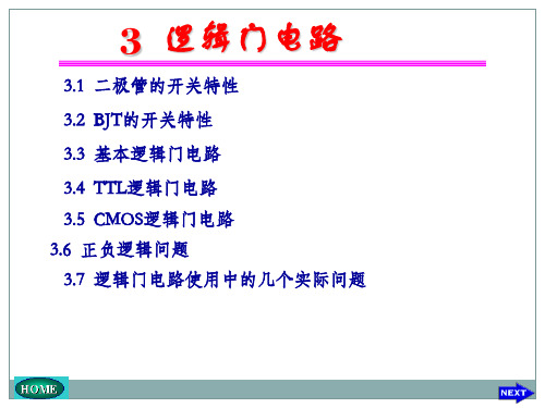
3.3.3 非门电路 ─ 三极管反相器
当输入为逻辑0时:
V CC
非逻辑真值表
Rc
0
A
Rb
T
vcc L
1
非逻辑真值表
输入A
0
输出L
1
24
3.3.3 非门电路 ─ 三极管反相器
17
VCC+(5V)
D1 A
D2 B
D3 C
R 3kW
L
二极管与门电路
A
&
B
L=A· B· C
C
与逻辑符号
3.3.1 二极管与门电路
若输入端中有任意一个 为0V,另两个为+5V
VCC+(5V)
0V D1
A
5V D2
B
5V D3
C
R 3kW
0v L
18 输入与输出电压关系
输
入
输出
VA 0 0 0 0 +5 V +5 V +5 V +5 V
11
1. BJT的开关作用
2. BJT的开关时间
3.2 BJT的开关特性
12
1. BJT的开关作用
IBS=VCC/Rc ICS= VCC/Rc CE=VCES≈0.2V
+-VVBB11 RRbb
数字电路ppt课件
主要的工具是逻辑代数,电路的功能用真值表、
逻辑表达式及波形图表示。
3
模拟电路研究的问题
基本电路元件: 基本模拟电路:
•晶体三极管 •场效应管 •集成运算放大器
• 信号放大及运算 (信号放大、功率放大) • 信号处理(采样保持、电压比较、有源滤波) • 信号发生(正弦波发生器、三角波发生器、…)
4
数字电路研究的问题
长中含反, 去掉反。
A B(A A) A B
例如:A ABC DE A BC DE
被吸收
32
3.混合变量的吸收: AB AC BC AB AC
证明: AB AC BC
1
AB AC (A A)BC
正负相对, 余全完。
AB AC ABC ABC AB AC
BA BD BC
38
吸收
例如: AB AC BCD AB AC BC BCD AB AC BC AB AC
33
五、摩根定理
AB AB AB AB
还有更多变量
可以用列真值表的方法证明:
A
B A•B A • B A
B AB
00 01
1
11
01 01
1
01
10 01
0
11
11 10
0
00
34
反演定理:将函数式 F 中所有的
C
开关断为逻辑“0”
E
F
灯亮为逻辑“1”
灯灭为逻辑“0”
20
E
真值表 AB 00 00 01 01 10 10 11 11
A B C
CF 00 11 01 11 01 11 01 11
真值表特点: 任1 则1, 全0则0。
数字电子技术基础(数字电路)第一章数字电路概述 ppt课件

来表示1 和 0
数字信号的描述:
高电平 低电平
v(t)
上升沿 下降沿
t
2. 数字集成电路的分类及特点
分类
按功能
组合型;时序型
按器件类型
TTL型; CMOS型
按集成度
小规模;中规模;大规模; 超大规模;甚大规模
分类
晶体管数量 典型器件/电路
小规模(SSI) 中规模(MSI)
几十以内 几百
逻辑门 加法器、计数器
三、补码及其运算
【例】设字长为4,分别写出+6、-6的原码、反码 和补码。
原码
反码
补码
+6 0 110 -6 1 110
0 110 1 001
0 110 1 010
补码怎么变回原码?
原码、反码、补码对照表
(字长为4)
思考
字长为n时原码、反码和 补码所能表示的数值范 围?
原码 (2n-1 1)~+(2n-1 1) 反码 (2n-1 1)~+(2n-1 1) 补码 2n-1 ~+(2n-1 1)
① (1010110.101)B = ( 86?.625 )D 计权相加
126+124+1 22 +121+121+123
思考
推广到任意进制转换成十进制?
② (37.706)D = ( 100101?.101101 )B
(37)D
(0.706)D
除2取余
乘2取整
(100101)B
(0.101101 )B
分组
代换
( 0101 1100 1011 . 0100 1000 )B
② (1F5. 6)H = ( 1111?10101.011 )B
数字电路 讲义 353f13dec04-slides-3x3

A¯B¯ , A¯B, AB¯ , AB, A¯C¯ , A¯C , AC¯ , AC , B¯ C¯ , B¯ C , BC¯ , BC .
As the number of input variables goes from 3 to 4 to 5 and beyond, the number of literals, minterms, and non-literalnon-minterm products gets very big, very fast.
ENEL 353 F13 Section 02 Slides for Lecture 36
What’s left in ENEL 353 in Fall 2013?
slide 4/21 ENEL 353 F13 Section 02 Slides for Lecture 36
PLAs: Programmable logic arrays
slide 9/21
What products are available? Let’s look at the example of a 3-input system with inputs A, B, C . All of the literals are products: A, A¯, B, B¯ , C , C¯ .
A key aspect of PLAs is the ability to select products with whatever number of literals makes sense.
A generic M × N × P PLA
inputs M
AND array
implicants N
Dot notation for PLAs (and ROM arrays)
数字电子技术教学课件-第01章 数字电路基础知识.ppt

入的数字信号进行各种算术运算和逻辑运算、逻辑
判断,故又称为数字逻辑电路。
2021/1/17
8
1.1.3 数字电路的分类和学习方法
1. 数字电路的分类
(1)按电路结构分类
组合逻辑电路:电路的输出信号只与当时 的输入信号有关,而与电路原来的状态无关。
时序逻辑电路:电路的输出信号不仅与当 时的输入信号有关,而且还与电路原来的状态 有关。
4
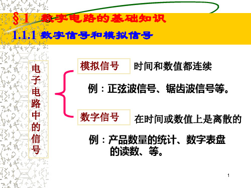
模拟信号: 时间上连续:任意时刻有一个相对的值。 数值上连续:可以是在一定范围内的任意值。 例如:电压、电流、温度、声音等。 真实的世界是模拟的。
缺点:很难度量; 容易受噪声的干扰; 难以保存。
优点:用精确的值表示事物。
模拟电路:处理和传输模拟信号的电路。
三极管工作在线性放大区。
2021/1/17
2021/1/17
9
(2)按集成电路规模分类
划分集成电路规模的标准
集成度:每块集成电路芯片中包含的元器件数目
数字集成电路
类别
➢小规模集成电路MO(SSmaIlCl
Sca双le极IICC,SS模I拟) 集成电路
➢中规模S集SI成电路<(M1e0d2ium Sc<al1e00IC,MSI)<30
➢大规模M集SI成电路10(2L~a1r0g3e Sc1a0l0e~5I0C0,LSI)30~100
2021/1/17
7
2. 数字电路特点(与模拟电路相比)
(1)数字电路的基本工作信号是用1和0表示的 二进制的数字信号,反映在电路上就是高电平和低 电平。
(2)晶体管处于开关工作状态,抗干扰能力强、 精度高。
(3)通用性强。结构简单、容易制造,便于集 成及系列化生产。
(4)具有“逻辑思维”能力。数字电路能对输
数字电路讲义 第三章

逻辑门电路
[例] 下图中,已知 ROFF 800 ,RON 3 k,试对应 输入波形定性画出TTL与非门的输出波形。
A 3.6 V 0.3 V
逻辑0 (a)
逻辑1
O Ya t
(b)
解:图(a)中,RI = 300 < ROFF 800 相应输入端相当于输入低电平, O 也即相当于输入逻辑 0 。 Yb 不同因此 TTLY 系列, R R 不同。 ON、 OFF UOH 。 a 输出恒为高电平 图(b)中,RI = 5.1 k > RON 3 k 相应输入端相当于输入高电平, O 也即相当于输入逻辑 1 。 Yb A 1 A 因此,可画出波形如图所示。
EXIT
逻辑门电路
一、三极管的开关作用及其条件
iC 临界饱和线 M T IC(sat) uI=UIH + uBE S Q
放大区
IB(sat)
饱 和 区
截止区
O UCE(sat) B uBE < Uth A N C uCE
三极管开通的条件和等效电路 当输入 uI 为高电平,使 iB ≥ IB(sat)时,三极管饱和。 uBE UCE(sat) 0.3 V 0, C、E 间相当于开关合上。
逻辑门电路
二、高电平和低电平的含义
高电平和低电平为某规定范围的电位值,而非一固定值。
3.6V 2.4V
1
高电平
0
高电平
高电平信号是多大的信号?低 由门电路种类等决定 电平信号又是多大的信号?
0.8V 0V
低电平
0
低电平
1
正逻辑体制
负逻辑体制
EXIT
逻辑门电路
3.2 三极管的开关特性
数字电路讲义

三变量: F(ABC)=/AF(0BC) + AF(1BC)
=/A/Bf (00C)+/ABf (01C)+A/Bf (10C)+ABf(11C)
三、逻辑代数常用公式
(一)常用公式:
1+A=A,A+/A=1
函数的化简 (二)“异或”运算公式: 定义: 表达式: 真值表: 符号: 物理意义: 公式: (三)“同或”运算公式:
=1
(二)最小项性质:
(三)标准与或表达式
每个与项都是最小项的与或表达式称为:标准与或表 达式;最小项之和;积之和;SOP 标准表达式的特点: 变换成标准形式后,通常会增加复杂度。 其权衡措施就是采用更多的结构化的方法来设计巨大 而复杂的逻辑网络 1.从真值表求标准与或表达式 例:三人表决逻辑
*最小项与最大项之间关系:
为什么从 (三)标准或与表达式: 真值表求函 每个或项都是最大项的或与表达式称为:标准或与表 数可以用最 达式;最大项之积;和之积;POS 大项之积表 1.从真值表求标准或与表达式 示? 2.从一般或与表达式求标准或与表达式
=0
1.从真值表求标准或与表达式 2.从一般与或表达式求标准与或表达式
第二章 逻辑函数及逻辑门
逻辑电路要 解决的问题? 1.逻辑分析 2.逻辑设计
1849年英国数学家乔治· 布尔(George Boole)首先提出了描述客 观事物逻辑的数学方法――布尔代数。 1938年克劳德· 香农(Claude E. Shannon)将布尔代数应用到继 电开关电路的设计,因此又称为开关代数。 随着数字技术的发展,布尔代数成为数字电路分析和设计的基础, 又称为逻辑代数。
1.从真值表求标准与或表达式
总结:将真值表中函数值为1所对应的最小项相加 2.从一般与或表达式求标准与或表达式
- 1、下载文档前请自行甄别文档内容的完整性,平台不提供额外的编辑、内容补充、找答案等附加服务。
- 2、"仅部分预览"的文档,不可在线预览部分如存在完整性等问题,可反馈申请退款(可完整预览的文档不适用该条件!)。
- 3、如文档侵犯您的权益,请联系客服反馈,我们会尽快为您处理(人工客服工作时间:9:00-18:30)。
AB =
1 if both A and B are 1 0 otherwise
Let’s write the truth table for AND.
ENEL 353 F13 Section 02 Slides for Lecture 6
ENEL 353 F13 Section 02 Slides for Lecture 6
slide 10/21 ENEL 353 F13 Section 02 Slides for Lecture 6
slide 11/21 ENEL 353 F13 Section 02 Slides for Lecture 6
This version uses unsigned binary encoding for positions 0 to 15. Why is this encoding a poor design choice?
If the light and dark markings on the spinning disk are organized using a Gray code, that eliminates the problem of having two or more bits change at almost but not exactly the same time.
ranges for two’s-complement systems overflow in two’s-complement addition BCD (binary coded decimal) codes for decimal digits Gray codes
A little more about Gray codes. Introduction to logic gates.
20 September, 2013
ENEL 353 F13 Section 02 Slides for Lecture 6
Previous Lecture
slide 2/21 ENEL 353 F13 Section 02 Slides for Lecture 6
Today’s Lecture
slide 3/21
The AND gate
Here is the symbol and the algebraic notation: A Y = AB B
One way to remember the symbol is to remember that the word AND contains a D, and the symbol looks like a D. An alternate algebraic notation for AND uses the · symbol, as in Y = A · B. Here is how the AND operation is defined:
slide 15/21
Truth tables
A truth table describes a combinational logic element by making a list of the values of the output for all possible combinations of input bits. (We’ve already seen the truth table for the 1-bit full adder.) Let’s write out the very simple truth tables for a NOT gate and a buffer.
A 4-bit shaft encoder: Optical sensors make a digital measurement of the rotation angle of a spinning metal disk. This could be used for a digital weathervane, indicating one of 16 wind directions N, NNE, NE, ENE, . . . , NNW.
A logic gate is a combinational logic circuit that has one or more inputs, each of which is a bit; exactly one output, which is a bit.
According to this definition, is the full adder a logic gate?
sliபைடு நூலகம்e 12/21
Graphical and algebraic notations for some common 1- and 2-input logic gates
A
Y =A
A
B
A
Y =A
A
A
B
B
Y = AB
A
A
B
B
Y =A+B
A
B
Y =A⊕B Y = AB Y =A+B Y =A⊕B
We’ll now examine these gates one or two at a time . . .
Very precise shaft encoders can measure very small changes in angles in industrial equipment. For example, a 12-bit shaft encoder measures rotation angle to within 360◦/212 = 0.088◦.
ENEL 353 F13 Section 02 Slides for Lecture 6
Combinational versus Sequential Logic
slide 7/21 ENEL 353 F13 Section 02 Slides for Lecture 6
slide 8/21 ENEL 353 F13 Section 02 Slides for Lecture 6
Slides for Lecture 6
ENEL 353: Digital Circuits — Fall 2013 Term
Steve Norman, PhD, PEng
Electrical & Computer Engineering Schulich School of Engineering University of Calgary
The outputs of a sequential logic circuit depend on the history of its input values.
A B Cin
full adder
Cout S
The values of Cout and S depend on what the values of A, B, and Cin are RIGHT NOW, not what they were a few minutes ago, or even a few nanoseconds ago.
ENEL 353 F13 Section 02 Slides for Lecture 6
Practical shaft encoders use Gray codes
slide 6/21
extra 0 not part of either code
n-bit Gray code
...
0
...
n-bit binary code
1-input gates
A NOT gate, also called an inverter:
A
Y =A
In A is the input and Y is the output. The “bubble” in the symbol indicates inversion: 0 converted to 1, and 1 converted to 0. The equation Y = A is read, “Y equals NOT A.”
Example combinational circuit: 1-bit full adder
What does the term logic gate mean?
slide 9/21
It’s IMPORTANT to know what these words mean.
The outputs of a combinational logic circuit depend only the current values of its inputs.
An alternate notation for the NOT operation
The “overline” is probably the most common notation for the NOT operation, but there is another symbol in wide use. Many textbooks and other documents use the symbol (“prime”) instead. This includes the textbook used last year in ENEL 353. This year we will use an “overline” for the NOT operation, to be consistent with this year’s textbook. If you see A in course material from past years, translate that in your head to A.