
Altera FPGA的特殊管脚的连接(中文)
FLEX 6000
-
All
输入
低有效芯片使能,本管脚使用低电平使能器件来允许配置,对于单芯片配置应当被固定为低电平,在配置以及初始化过程和用户模式,本管脚必须固定为低电平;在级联时,第一片的nCE接地,前一片的nCEO接后一片的nCE;
nCEO
APEX II
APEX 20K
Mercury
ACEX 1K
FLEX 10K
-
级联
输出
当设备配置完成后被驱动为低电平。在多器件配置过程中,这个管脚用来连接后面器件的nCE引脚,最后一片的nCEO悬空;
FLEX 6000
I/O
nWS
APEX II
APEX 20K
Mercury
ACEX 1K
FLEX 10K
1特殊管脚
2用户I/O
并行异步模式
输入
写选通输入:对于APEX II、Mercury、ACEX 1K、APEX 20K和FLEX 10K器件0-1的跳变引起器件锁存一个字节的数据在DATA[7..0]引脚;对于FLEX 6000器件,一个0-1的跳变会引起器件锁存一个位的数据在DATA引脚。
APEX 20K
Mercury
ACEX 1K
FLEX 10K
FLEX 6000
特殊管脚不能做用户I/O
All
双向
集电极开路
状态输出:
在配置之前和配置过程中,器件驱动本管脚为0,一旦所有配置数据都被接收并没有错误发生,则初始化时钟周期开始时器件释放本管脚;
状态输入:在所有数据被接收后,本管脚为高电平,器件初始化,然后进入用户模式;
APEX 20K
Mercury
ACEX 1K
FLEX 10K
FLEX 6000
-
1配置器件
2串行加载
3并行同步模式
输入
时钟输入,用于从一个外部信号源输入时钟数据进入器件,在串行异步模式或并行异步模式
配置中, DCLK应当被拉高,不能悬空;
nCE
APEX II
APEX 20K
Mercury
ACEX 1K
ALTERA FPGA特殊管脚说明、
管脚名称
器件系列
使用模式
配置模式
管脚类型
描述
MSEL0
MSEL1
APEX II
APEX 20K
Mercury
ACEX 1K
FLEX 10K
特殊管脚不能做用户I/O
All
输入
设置APEX II、Mercury、ACEX 1K、APEX 20K和FLEX 10K器件配置模式
APEX II
APEX 20K
Mercury
ACEX 1K
FLEX 10K
FLEX 6000
1器件级的清零
2用户I/O
All
输入
此管脚需要在编译设置中设定才能实现第一功能,缺省是第二功能;
当本引脚被拉低,所有寄存器被清除。
当本引脚被拉高,所有寄存器都处于程序控制状态。
TDI
APEX II
APEX 20K
DEV_OE
APEX II
APEX 20K
Mercury
ACEX 1Kቤተ መጻሕፍቲ ባይዱ
FLEX 10K
FLEX 6000
1器件级的使能
2用户I/O
All
输入
此管脚需要在编译设置中设定才能实现第一功能,缺省是第二功能;
当本引脚被拉低,所有I/O都是三态。
当本引脚被拉高,所有I/O在正常的程序控制状态。
DEV_CLRn
Mercury
ACEX 1K
FLEX 10K
FLEX 6000
1器件级的使能
2用户I/O
All
输出
集电极开路
状态管脚:可以被用来指示器件已经被初始化或者已经进入用户模式;在配置过程中INIT_DONE引脚保持低电平,在初始化之前和之后,INIT_DONE引脚被释放,被上拉到VCCIO通过一个外部上拉电阻,因为INIT_DONE在配置之前是三态,所以被外部的上拉电阻拉到高电平。因此监控电路必须能够检测一个0-1的跳变信号。这个选项可以在MAX+PLUS II或Quartus II软件中被设置。
本管脚必须通过一个1K的电阻上拉到VCCIO
(APEX 20KE或APEX 20KC器件使用10K欧姆电阻)
外部的信号源可以驱动本管脚为低,来延迟初始化的过程,当使用一个配置器件进行配置除外,
在配置以及初始化之后,驱动本管脚为低,不影响配置器件。
(详细见AN116中的配置时序)
DCLK
APEX II
FLEX 10K
1特殊管脚
2用户I/O
1并行异步模式
2串行异步模式
输入
数据输入:并行的字节流数据通过DATA[7..1]与DATA0输入器件;
DATA0
APEX II
APEX 20K
Mercury
ACEX 1K
FLEX 10K
特殊管脚不能做用户I/O
配置器件
PS
PPA
PPS
输入
数据输入:在串行配置模式下比特流数据通过DATA0写入器件;
FLEX 6000
1特殊管脚
2用户I/O
串行异步模式
nRS
APEX II
APEX 20K
Mercury
ACEX 1K
FLEX 10K
1特殊管脚
2用户I/O
并行异步模式
输入
读选通输入:对于APEX II、Mercury、ACEX 1K、APEX 20K和FLEX 10K器件低电平表示在DATA7引脚输出的是RDYnBSY信号;对于FLEX 6000器件,低电平表示在DATA引脚输出的是RDYnBSY信号,如果nRS管脚没有使用,应该被固定连接到高电平。
1配置器件
2串行加载
3串行异步加载
输入
数据输入:对FLEX 6000器件来说串行的配置数据是出现在DATA引脚,在串行异步加载方式下,nRS信号被锁存之后DATA管脚上出现的是RDYnBSY信号;
(详细见AN116中的PSA配置时序)
DATA[7..1]
APEX II
APEX 20K
Mercury
ACEX 1K
如果在配置过程中,如有错误发生,本管脚被器件拉;。
如果在配置或初始化过程中,有一个外部的信号源驱动本管脚为低,则器件进入一个错误的状态;
在配置或初始化之后,驱动本管脚为低,不会影响器件。但是,如果使用专用配置器件,驱动本管脚低将引起配置器件试图去配置APEX或FLEX器件。
(详细见AN116中的配置时序)
CLKUSR
APEX II
APEX 20K
Mercury
ACEX 1K
FLEX 10K
FLEX 6000
1特殊管脚
2用户I/O
All
输入
可选的用户时钟输入信号:用在初始化过程中;
(注:在初始化过程中可以继续使用配置数据用的DCLK,或者切换到用CLKUSR)
DATA
FLEX 6000
特殊管脚不能做用户I/O
MSEL1 MSEL0配置模式
0 0串行配置或使用配置器件模式10并行同步模式
1 1并行异步模式
MSEL
FLEX 6000
特殊管脚不能做用户I/O
All
输入
MSEL配置模式
0串行加载或使用加载器件模式,及MasterBlaster或ByteBlasterMV加载电缆模式
1串行异步模式
nSTATUS
APEX II
FLEX 6000
1特殊管脚
2用户I/O
串行异步模式
RDYnBSY
APEX II
APEX 20K
Mercury
ACEX 1K
FLEX 10K
FLEX 6000
1特殊管脚
2用户I/O
1并行异步模式
2串行异步模式
输出
忙闲信号:高电平表示器件准备好来存取另外字节的数据;高电平表示器件没有准备好接收另外字节的数据。
Mercury
ACEX 1K
FLEX 10K
FLEX 6000
1JTAG
2用户管脚
All
输入
JTAG引脚。当被用作为用户I/O引脚的时候,
JTAG引脚电平必须保持稳定,在配置之前和配置过程中。JTAG引脚稳定性可以预防意外的装载JTAG指令。
TDO
输出
TMS
输入
TCK
输入
nCS
CS
APEX II
APEX 20K
Mercury
ACEX 1K
FLEX 10K
FLEX 6000
1特殊管脚
2用户I/O
1并行异步模式
2串行异步模式
输入
片选择信号:nCS为低电平且CS为高电平器件被使能可以进行配置,如果只有一个芯片选择输入被使用,那么另外一个必须被激活,(举例来说:如果只用CS作为片选择信号则nCS必须被连接到地),在配置和初始化的过程中,nCS和CS管脚必须被处于有效状态,
DATA7
APEX II
APEX 20K
Mercury
ACEX 1K
FLEX 10K
1特殊管脚
2用户I/O
PPA
输出
在PPA配置方式,DATA的数据是被RDYnBSY信号通过电平触发方式在nRS信号已经被锁存之后写入;
(详细见AN116中的PPA配置时序)
INIT_DONE
APEX II
APEX 20K
APEX 20K
Mercury
ACEX 1K
FLEX 10K
Altera的FPGA_常见问题汇总

常见问题汇总1. alt2gxb模块的每个发送端都需要一个高速的pll_inclk时钟(至少100M以上),请问这个时钟一定要从FPGA外面引进来吗?通常情况下一定要从FPGA外面引进来,首选是GXB模块的专用时钟引脚,或上下BANK 的专用时钟输入脚。
时钟是至少60M以上。
2. 如果我一个FPGA里面有多个alt2gxb模块,是否能共用一个这样的输入时钟?可以。
3. gxb模块里面的Calibration clk 是干嘛用的,能不能不用它?校准内部匹配电阻用。
此时钟可以内部提供,频率在10M到125M都可以,如果外部时钟不合适的话,甚至可以用逻辑来分频(比如参考钟是156M,内部触发器作个2分频就可以用了。
4. 用到gxb模块的bank的参考电压是否必须接1.5V?因为我看到资料上有3.3V的CML和LVDS电平(附件里面的截图)gxb用1.5V 或 1.2V, 推荐客户用1.5V. 3.3v是用在别的普通bank的。
5. gxb模块的输入端如果平时不需要传数据,是否置0?还是需要我们在数据线上发送别的数据,是否gxb模块能自动发送同步码?平时可以置0,但在上电后,你必须首先发送对端接收侧的word aligner码型(通常用k28.5), 这是需要手工控制的。
6. LVDS模块没有同步码,做接收时好像没办法数据对其,比如8比特数据容易错开2、3位,我们现在是另外加逻辑把它调整过来的,请问有别的好的同步的方法吗通常需要逻辑去进行word aligner操作,如同GXB一样。
某些特定情况下可以预先知道边界。
这个问题讨论过好多次了,所谓的特定情况你可以看STRATIX II手册(不是Stratix II GX 手册),搜索“Differential I/O Bit Position”7.请问在alt2gxb模块,有两个时钟:pll_inclk和cali_clk,手册上说cali_clk要求不是很高,可以用计数器产生,那么输入的并行数据txdata_in应该用哪个时钟锁存呢?cali_clk仅用于校准内部匹配电阻用的状态机,跟业务是完全独立的。
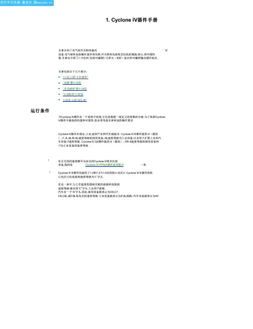
EP4CE15M8I7N中文资料(Altera)中文数据手册「EasyDatasheet - 矽搜」
VCCINT (3) VCCA (1), (3) VCCD_PLL (2)
VCCIO (3), (4)
VCC_CLKIN
(3), (5), (6)
核心电压,PCIe硬核IP模块,和 收发器PCS电源
PLL模拟电源
PLL数字供电
3.3 I / O插槽电源
-V
手术
3.0 I / O插槽电源
-V
手术
2.5 I / O插槽电源
供应1.5 -V工作电压
差分时钟输入引脚电源
供应1.2 -V工作电压
条件
— — — — — — — — — — — — — — —
Min Typ Max Unit
1.16 1.2 1.24 V
2.375 2.5 2.625 V
1.16 1.2 1.24
V
3.135 3.3 3.465 V
2.85
3
3.15
电源电压为输出缓冲器, 3.3-V操作
电源电压为输出缓冲器, 3.0-V操作
电源电压为输出缓冲器, 2.5-V操作
电源电压为输出缓冲器, 1.8-V操作
电源电压为输出缓冲器, 1.5-V操作
电源电压为输出缓冲器, 1.2-V操作
供应(模拟)电压PLL
调节器
VCCD_PLL (3)
VI VO
供应(数字)电压PLL, 1.2-V操作
–0.5 —
3.6
V
0
—
VCCIO
V
0
—
85
°C
–40
—
100°C(5) –0—125°C
–40
—
125
°C
50 µs — 50毫秒 —
50 µs —
(50条消息)Altera特殊管脚的使用(适用全系列AlteraFPGA,MSEL区别除外)

(50条消息)Altera特殊管脚的使用(适用全系列AlteraFPGA,MSEL区别除外)1.I/O, ASDO在AS 模式下是专用输出脚,在PS 和JTAG 模式下可以当I/O 脚来用。
在AS 模式下,这个脚是CII 向串行配置芯片发送控制信号的脚。
也是用来从配置芯片中读配置数据的脚。
在AS 模式下,ASDO 有一个内部的上拉电阻,一直有效,配置完成后,该脚就变成三态输入脚。
ASDO 脚直接接到配置芯片的ASDI 脚(第5 脚)。
2.I/O,nCSO在AS 模式下是专用输出脚,在PS 和JTAG 模式下可以当I/O 脚来用.在AS 模式下,这个脚是CII 用来给外面的串行配置芯片发送的使能脚。
在AS 模式下,ASDO 有一个内部的上拉电阻,一直有效。
这个脚是低电平有效的。
直接接到配置芯片的/CS 脚(第1 脚)。
3.I/O,CRC_ERROR当错误检测CRC 电路被选用时,这个脚就被作为CRC_ERROR 脚,如果不用默认就用来做I/O。
但要注意,这个脚是不支持漏极开路和反向的。
当它作为CRC_ERROR 时,高电平输出则表示出现了CRC 校验错误(在配置SRAM 各个比特时出现了错误)。
CRC 电路的支持可以在setting 中加上。
这个脚一般与nCONFIG 脚配合起来用。
即如果配置过程出错,重新配置.4.I/O,CLKUSR当在软件中打开Enable User-supplled start-up clock(CLKUSR)选项后,这个脚就只可以作为用户提供的初始化时钟输入脚。
在所有配置数据都已经被接收后,CONF_DONE 脚会变成高电平,CII 器件还需要299 个时钟周期来初始化寄存器,I/O 等等状态,FPGA 有两种方式,一种是用内部的晶振(10MHz),另一种就是从CLKUSR 接进来的时钟(最大不能超过100MHz)。
有这个功能,可以延缓FPGA 开始工作的时间,可以在需要和其它器件进行同步的特殊应用中用到。
fpga配特殊引脚的含义(FPGAwiththemeaningofaspecialpin)
fpga配特殊引脚的含义(FPGA with the meaning of a special pin)FPGA with the meaning of a special pin1.I/O, ASDOIn AS mode, it is dedicated output pin, and can be used as I/O pin in PS and JTAG mode. In AS mode, this pin is the CII pin that sends the control signal to the serial configuration chip. Also used to read configuration data from the configuration chip. In AS mode, the ASDO has an internal pullup resistor, which has been in effect until the configuration is completed, and the pin becomes a three state input pin. The ASDO pin is connected directly to the ASDI pin (fifth feet) of the configuration chip.2.I/O, nCSOIn AS mode, it is a dedicated output pin that can be used as the I/O pin in PS and JTAG mode. In AS mode, this pin is used by the CII to send the enable pins to the outside serial configuration chip. In AS mode, the ASDO has an internal pullup resistor that has been in effect. This pin is active low. The /CS pin (first feet) is directly connected to the configuration chip.3.I/O, CRC_ERRORWhen the error detection CRC circuit is selected, this foot is used as the CRC_ERROR pin, and if not used by default, it is used as I/O. Note, however, that this pin does not support open drain and reverse. When it is used as CRC_ERROR, the high leveloutput indicates a CRC checksum error (when an individual bit of the SRAM is configured). CRC circuit support can be added to the setting. This foot is usually used with the nCONFIG foot. That is, if the configuration process is wrong, reconfigure it4.I/O, CLKUSRWhen the Enable User-supplled start-up clock (CLKUSR) option is opened in the software, this pin can only be used as an initialization clock input for the user. In all configuration data have been received, CONF_DONE pin will become a high level, the CII device 299 clock cycles are needed to initialize the I/O register, FPGA and so on, there are two ways, one is using the internal oscillator (10MHz), another is from CLKUSR in the clock (maximum not more than 100MHz). This feature can delay the time FPGA starts working and can be used in special applications that require synchronization with other devices.5.I/O, VREFUsed to provide a reference level for certain differential standards. If not used, you can use it as a I/O.6. DATA0Dedicated input pin. In AS mode, the configuration process is: CII sets the nCSO low, and the configured chip is enabled. CII then cooperates with DCLK and ASDO to send commands and read addresses to the configuration chip. Configure the chip and then send the data to the CII via the DATA pin. The DATA foot is attached to the CII's DATA0 foot. After all configurationdata is received by the CII, the CONF_DONE pin is released (that is, the CONF_DONE pin is not forced low) and the CONF_DONE pin is open drain (Open-Drain). At this point, the 10K will turn on a high level because the CONF_DONE will pick up a resistor on the outside. At the same time, the CII stops the DCLK signal. After the CONF_DONE becomes high (when it becomes equivalent to an input pin), the initialization process begins. So, CONF_DONE must have a 10K resistor on the outside of the foot to ensure that the initialization process starts correctly. DATA0, DCLK, NCSO, and ASDO have weak pullup resistors on their feet, and they are always valid. Upon completion of the configuration, these pins are turned into an input three state, and the level is set to a high level by an internal pullup resistor. In AS mode, the DATA0 receives the DATA (second pin) of the configuration chip.7. DCLKPS mode is input, AS mode is output. In PS mode, the DCLK is a clock input pin that is the clock that the external device sends the configuration data to the FPGA. Data is placed on the rising edge of the DCLK to data in AS mode, and the DCLK pin is a clock output pin that is configured to provide a clock. Connect directly to the DCLK pin of the configuration chip (sixth feet). No matter what configuration mode, after the configuration is completed, this foot will become three states. If an external configuration device is attached, the configuration device will set the DCLK pin to low level. If you are using the master chip, you can either set the DCLK high or you can lower the DCLK. When the configuration is complete, triggering this pin does not affect the configured FPGA. Thispin has an input Buffer that supports the hysteresis function of the Schmidt flip-flop.8. nCEDedicated input pin. This pin is an active low chip enable signal. The nCE pin is configured to enable the foot. In configuration, initialization, and user mode, the nCE pin must be set low. In the configuration of multiple devices, the nCE pin of the first device is set low, and its nCEO is connected to the nCE pin of the next device, forming a chain. The nCE pin also requires a low nCE foot in the JTAG programming mode.This pin has an input Buffer that supports the hysteresis function of the Schmidt flip-flop.9. nCONFIGDedicated input pins. This pin is a configuration control input pin. If this foot is low in user mode, the FPGA loses its configuration data and goes into a reset state and sets all the I/O feet into three states. The process of changing nCONFIG from low level to high level will initialize the reconfiguration process. If the configuration scheme uses an enhanced configuration device or EPC2, the user can connect the nCONFIG pin directly to the VCC or to the nINIT_CONF pin of the configuration chip. This pin has an input Buffer that supports the hysteresis function of the Schmidt flip-flop. In fact, in user mode, the nCONFIG signal is used to initialize the reconfiguration. When the nCONFIG foot is low, the initialization process begins. When the nCONFIG pin is low, theCII is reset and goes into the reset state. The nSTATUS and CONF_DONE pins are set low and all the I/O pins are in the three state. The nCONFIG signal must remain at least 2us. When nCONFIG returns to the high level state, the nSTATUS is released again. The reconfiguration starts. In actual application, the nCONFIG pin can be connected with a pull-up resistor of 10K to 3.3V.10. DEV_OEI/O pin or global I/O enable pin. In the Quartus II software can enable the DEV_OE option (Enable Device-wideoutput Enable), if can make this a function, this pin can be enabled when the global I/O feet, this foot function is, if it is set low, all I/O into three states.11. INIT_DONEI/O pin or drain open output pin. When this foot is enabled, the foot jumps from low to high, indicating that the FPGA has entered the user mode. If the INIT_DONE output pin is enabled, this pin cannot be used as user I/O after configuration is complete. Inside the QuartusII, this pin can be enabled by enabling the Enable INIT_DONE output option.12. nCEOI/O pin or output pin. When the configuration is complete, this pin outputs low level. In the configuration of multiple devices, this pin will connect to the next device's nCE pin. This time, it also needs a 10K pull-up resistor outside to Vccio. The configuration process of multiple devices, finally a nCEOdevice can float. If you want to use this pin as an available I/O, you need to set it up inside the software. In addition, even if the I/O, but also after the completion of the configuration.13. nSTATUSThis is a dedicated configuration status pin. Two way foot, when it is the output pin, is open drain. After power on, the FPGA immediately sets the nSTATUS foot low and releases it after power on reset (POR) and sets it high. As a status output pin, if any error occurs during configuration, the nSTATUS pin is lowered. As the status input pin, during the configuration or initialization, the external control chip can pull this pin down, and FPGA will enter the wrong state at this time. This foot can not be used as an ordinary I/O foot. The nSTATUS pin must be pulled up by a 10K ohm resistor.14. CONF_DONEThis is a dedicated configuration status pin. Two way foot, when it is the output pin, is open drain. When it is used as a status output pin, it is set low before and during configuration. Once the configuration data is received and no errors are made, the CONF_DONE will be released at the start of the initialization cycle. When used as a status input pin, after all data has been received, it should be set to a high level. After that, the device starts initialization and goes into user mode. It should not be used as a regular I/O. The outside of the foot must also be connected with a 10K ohm resistor.15. MSEL[1:0]These pins should be connected to zero or power, indicating high or low level. 00 with AS mode, 10 PS mode, AS mode is 01 FAST. If in JTAG mode, it with their 00 JTAG mode and the MSEL has nothing to do with JTAG mode, MSEL will be ignored, but because they can not float, so suggest that it be received.16 DEV_CLRnI/O or global clear input. In QuartusII, if you choose the Enable Device-Wide Reset (DEV_CLRn) this function. This pin is the global reset. When this pin is low, all registers are cleared. This pin does not affect the JTAG's boundary scan or programming operations.Application of FPGA configuration pinFor FPGA applications, you need to know the following points.The nCONFIG, nSTATUS, and CONF_DONE require the pull-up resistor of the 10K, and the nCE requires a 10K pull-down resistor;NCONFIG for configuration control, the dedicated input pin sets the low FPGA to lose data;The nSTATUS is a dedicated bidirectional pin for the FPGA. 0 indicates that the FPGA is in a busy state and is released at 1 after the pull-up, and the FPGA begins to be in configuration.CONF_DONE dedicated configuration, two-way feet, FPGA configuration is 0, after the configuration is released, the role of the external pull-up is 1. NCE configuration enables dedicated input pins. In configuration, initialization, and user mode, the nCE pin must be set low.MSEL configure pin for mode;TDI, TMS, 10K pull-up resistor, TCK, 10K pull-down resistor, for JTAG;ASDO, nCSO, DCLK and DATA0 are used for the communication between FPGA and configuration chip, and there is no pullup on the inside, and no external resistance is needed.The clock pin can only be input and cannot be output.6 、 pull / pull resistance:1) ensure that the initial values of the circuit. For example, TCK signal using a pull-down resistor. Why the pull-down resistor instead of the pull-up resistor? Because pull-down resistor makes the initial value of the TCK signal is 0, because it is a clock signal, can guarantee the clock signal in the initial value after the first rise along the edge, and the JTAG control of resistance it is on the rising edge of TCK to write configuration data within the FPGA.2) here / pull-down resistor only belongs to the recommended value, determine the value is not, the purpose is to ensure the quality of the signal. The resistance as an example, if thepull-up resistor is above 10K, the pin has an equivalent capacitance to ground, because T=RC, C by the device process, the greater the resistance, charge and discharge the longer the time, the rising edge of the slower signal, the slope is small. The rise time if more than JTAG control circuit requirements to write data within the FPGA may be wrong. So, if the pull-up resistor smaller? Will rise time smaller? Yes. Resistance decreases, rise time small, the slope becomes larger, but also brought a serious problem, if the resistance is small to a certain extent, the signal will be at the rising edge of the emergence of the red signal ringing phenomenon, will seriously. If the resistance is too small, the intrusion tolerance over current devices IO, JTAG control circuit Will burn out. So, what is the resistance to meet the general requirements of PCB using 4.7K. in general?3) to ensure the driving ability of signal. As mentioned earlier, the resistance is small, the signal slope is small, and the driving force of signals is stronger. The more resistance signal slope is bigger, and the driving force of signals is weak. This point in the JTAG daisy chain circuit and its important。
fpga与gpio连接的原理
fpga与gpio连接的原理FPGA与GPIO连接的原理引言:FPGA(Field Programmable Gate Array)是一种可编程逻辑器件,它具有高度的灵活性和可重构性,可以实现各种不同的数字电路功能。
而GPIO(General Purpose Input/Output)则是一种通用输入输出接口,可以与外部设备进行数据交互。
本文将探讨FPGA与GPIO之间的连接原理。
一、FPGA的基本结构和工作原理FPGA由可编程逻辑单元(PL)和配置逻辑单元(CLB)组成。
PL负责实现特定的逻辑功能,而CLB则用于存储和配置逻辑单元的信息。
FPGA的工作原理是通过对配置逻辑单元进行重新编程,实现不同的电路功能。
FPGA芯片上有一组可编程管脚,可以与外部设备进行连接。
二、GPIO的基本概念和作用GPIO是一种通用的输入输出接口,可以用于与外部设备进行数据交互。
它可以通过编程的方式控制输入输出的电平状态,实现与外部设备的通信。
GPIO通常包含一组输入引脚和一组输出引脚,可以根据需要进行配置和使用。
三、FPGA与GPIO的连接方式FPGA与GPIO的连接方式有多种,下面将介绍两种常见的连接方式。
1. 直接连接方式最简单的方式是直接将FPGA的管脚与GPIO的引脚进行连接。
在使用之前,需要对FPGA的管脚进行配置,使其与GPIO的引脚相对应。
这种连接方式简单直接,适用于只需要少量IO口的应用场景。
2. 通过扩展芯片连接方式当需要连接大量的GPIO引脚时,可以使用扩展芯片来实现。
扩展芯片可以扩展FPGA的IO口数量,通过串行或并行的方式与FPGA进行连接。
对于大规模的应用,这种连接方式更加灵活可扩展。
四、FPGA与GPIO连接的步骤下面将介绍FPGA与GPIO连接的基本步骤。
1. 确定连接引脚需要确定FPGA上与GPIO连接的管脚和GPIO上的引脚。
这需要根据具体的FPGA和GPIO的规格书来确定。
2. 配置FPGA管脚根据连接引脚的确定,需要对FPGA上的管脚进行配置。
FPGA器件管脚说明

FPGA器件管脚说明用户I/O:不用解释了。
配置管脚:MSEL[1:0] 用于选择配置模式,比如AS、PS等。
DA TA0 FPGA串行数据输入,连接到配置器件的串行数据输出管脚。
DCLK FPGA串行时钟输出,为配置器件提供串行时钟。
nCSO(I/O)FPGA片选信号输出,连接到配置器件的nCS管脚。
ASDO(I/O)FPGA串行数据输出,连接到配置器件的ASDI管脚。
nCEO 下载链期间使能输出。
在一条下载链中,当第一个器件配置完成后,此信号将使能下一个器件开始进行配置。
下载链上最后一个器件的nCEO悬空。
nCE 下载链器件使能输入,连接到上一个器件的nCEO,下载链的最后一个器件nCE接地。
nCNFIG 用户模式配置起始信号。
nSTATUS 配置状态信号。
CONF_DONE 配置结束信号。
电源管脚:VCCINT 内核电压。
130nm为1.5V,90nm为1.2V。
VCCIO 端口电压。
一般为3.3V,还可以支持多种电压,5V、1.8V、1.5V。
VREF 参考电压。
GND 信号地。
时钟管脚:VCC_PLL PLL管脚电压,直接连VCCIO。
VCCA_PLL PLL模拟电压,截止通过滤波器接到VCCINT上。
GNDA_PLL PLL模拟地。
GNDD_PLL PLL数字地。
CLK[n] PLL时钟输入。
PLL[n]_OUT PLL时钟输出。
特殊管脚:VCCPD 用于寻则驱动。
VCCSEL 用于控制配置管脚和PLL相关的输入缓冲电压。
PROSEL 上电复位选项。
NIOPULLUP 用于控制配置时所使用的用户I/O的内部上拉电阻是否工作。
TEMPDIODEN 用于关联温度敏感二极管。
************************************************************************************1/1、I/O, ASDO在AS模式下是专用输出脚,在PS和JTAG模式下可以当I/O脚来用。
FPGA的引脚配置
Mercury
ACEX 1K
FLEX 10K
FLEX 6000
特殊管脚不能做用户I/O
All
双向
集电极开路
上电后被器件拉低,在5US之内,被器件释放,
(当使用一个专用配置器件时,专用加载器件将控制这个脚为低长达200ms。)这个管脚必须通过一个1K电阻上拉到VCCIO;
(APEX 20KE或APEX 20KC器件为10K欧姆)
ALTERA FPGA 特殊管脚说明、
管脚名称
器件系列
使用模式
配置模式
管脚类型
描述
MSEL0
MSEL1
APEX II
APEX 20K
Mercury
ACEX 1K
FLEX 10K
特殊管脚不能做用户I/O
All
输入
设置APEX II、Mercury、ACEX 1K、APEX 20K和FLEX 10K器件配置模式
nCS
CS
APEX II
APEX 20K
Mercury
ACEX 1K
FLEX 10K
FLEX 6000
1特殊管脚
2用户I/O
1并行异步模式
2串行异步模式
输入
片选择信号:nCS为低电平且CS为高电平器件被使能可以进行配置,如果只有一个芯片选择输入被使用,那么另外一个必须被激活,(举例来说:如果只用CS作为片选择信号则nCS必须被连接到地),在配置和初始化的过程中,nCS和CS管脚必须被处于有效状态,
Mercury
ACEX 1K
FLEX 10K
FLEX 6000
1JTAG
2用户管脚
All
输入
JTAG引脚。当被用作为用户I/O引脚的时候,
AlteraFPGA和Xilinx-FPGA-引脚功能详解解读
XilinxFPGA引脚功能详细介绍注:技术交流用,希望对大家有所帮助。
IO_LXXY_# 用户IO引脚XX代表某个Bank内唯一的一对引脚,Y=[P|N]代表对上升沿还是下降沿敏感,#代表bank号2.IO_LXXY_ZZZ_# 多功能引脚ZZZ代表在用户IO的基本上添加一个或多个以下功能。
Dn:I/O(在readback期间),在selectMAP或者BPI模式下,D[15:0]配置为数据口。
在从SelectMAP读反馈期间,如果RDWR_B=1,则这些引脚变成输出口。
配置完成后,这些引脚又作为普通用户引脚。
D0_DIN_MISO_MISO1:I,在并口模式(SelectMAP/BPI)下,D0是数据的最低位,在Bit-serial模式下,DIN是信号数据的输入;在SPI模式下,MISO是主输入或者从输出;在SPI*2或者SPI*4模式下,MISO1是SPI总线的第二位。
D1_MISO2,D2_MISO3:I,在并口模式下,D1和D2是数据总线的低位;在SPI*4模式下,MISO2和MISO3是SPI总线的MSBs。
An:O,A[25:0]为BPI模式的地址位。
配置完成后,变为用户I/O 口。
AWAKE:O,电源保存挂起模式的状态输出引脚。
SUSPEND是一个专用引脚,AWAKE是一个多功能引脚。
除非SUSPEND模式被使能,AWAKE 被用作用户I/O。
MOSI_CSI_B_MISO0:I/O,在SPI模式下,主输出或者从输入;在SelectMAP模式下,CSI_B是一个低电平有效的片选信号;在SPI*2或者SPI*4的模式下,MISO0是SPI总线的第一位数据。
FCS_B:O,BPI flash 的片选信号。
FOE_B:O,BPI flash的输出使能信号FWE_B:O,BPI flash 的写使用信号LDC:O,BPI模式配置期间为低电平HDC:O,BPI模式配置期间为高电平CSO_B:O,在并口模式下,工具链片选信号。
Altera FPGA加密中文
Altera 公司 2011年6月Subscribe© 2011 Altera Corporation. All rights reserved. ALTERA, ARRIA, CYCLONE, HARDCOPY, MAX, MEGACORE, NIOS, QUARTUS and STRATIX are Reg. U.S. Pat. & Tm. Off. and/or trademarks of Altera Corporation in the U.S. and other countries. All other trademarks and service marks are the property of their respective holders as described at /common/legal.html . Altera warrants performance of its semiconductor products to current specifications in accordance with Altera’s standard warranty, but reserves the right to make changes to any products and services at any time without notice. Altera assumes no responsibility or liability arising out of the application or use of any information, product, or service described herein except as expressly agreed to in writing by Altera. Altera customers are advised to obtain the latest version of device specifications before relying on any published information and before placing orders for products or services.101 Innovation DriveSan Jose, CA 使用Altera FPGA 中的设计安全特性本应用笔记介绍了如何使用 Altera ® 40-和28-nm FPGA 中的设计安全特性来保护您的设计免受非法复制、逆向工程以及配置文件的篡改。
Altera FPGA特殊管脚连接
如果在配置或初始化过程中,有一个外部的信号源驱动本管脚为低,则器件进入一个错误的状态;
在配置或初始化之后,驱动本管脚为低,不会影响器件。但是,如果使用专用配置器件,驱动本管脚低将引起配置器件试图去配置APEX或FLEX器件。
(详细见AN116中的配置时序)
APEX II
APEX 20K
Mercury
ACEX 1K
FLEX 10K
FLEX 6000
1器件级的清零
2用户I/O
All
输入
此管脚需要在编译设置中设定才能实现第一功能,缺省是第二功能;
当本引脚被拉低,所有寄存器被清除。
当本引脚被拉高,所有寄存器都处于程序控制状态。
TDI
APEX II
APEX 20K
本管脚必须通过一个1K的电阻上拉到VCCIO
(APEX 20KE或APEX 20KC器件使用10K欧姆电阻)
外部的信号源可以驱动本管脚为低,来延迟初始化的过程,当使用一个配置器件进行配置除外,
在配置以及初始化之后,驱动本管脚为低,不影响配置器件。
(详细见AN116中的配置时序)
DCLK
APEX II
nCONFIG
APEX II
APEX 20K
Mercury
ACEX 1K
FLEX 10K
FLEX 6000
特殊管脚不能做用户I/O
All
输入
配置控制引脚:
由0-1的跳变开始配置,由1-0跳变则复位器件;当设定本管脚为0时,所有I/O为三态。
(详细见AN116中的配置时序)
CONF_DONE
APEX II
APEX 20K