
比例放大器(VT-3013、3014)
插头式比例阀放大器
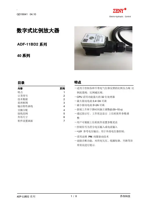
整 -用户可根据上位机软件设置参数更改 -控制信号为差分电压输入或电流输入 -+10V 参考电压输出,用于外部电位器控制。
3/8
ADF-11BD2 系列
1 U+ 外部电源
2 0V
5 控制信 IN(+) 号输入 IN(-)
4
DA RS485 DB
SG
3 +10VDC
PWM I a+
U
a32位微处理器
比例阀
MCU
6 1V=1A
与4脚IN-,测 量电压信号
ZENY ®
Electro-hydraulic Control
QD18041 04.10
ADF-11BD2 系列
7/8
乔存科技
ZENY ®
Electro-hydraulic Control
备注
QD18041 04.10
成都乔存科技有限公司 地址:成都市青羊区光华北三路 98 号 D 座 D1008 号 邮编:610031 电话:86-28-65933311(商务部)
86-28-61709123(技术部) 传真:86-28-65933311 网址: Email:sales@
U 0~+10 V Ri 100 KΩ
< 10 mV < 10 mV
I 4~20mA <0.01mA
U Ioutmax
Idrift
+10 V, 10 mA < 20 mV < 0.15 mA/℃
VICKERS数字放大器美国威格士VICKERS比例放大器用于
VICKERS数字放大器/美国威格士VICKERS比例放大器,用于带电位置反馈的比例阀欧洲卡制式的数字放大器下列阀均可重置所有参数:规格为6和10(元件系列为2X)的4WRE的阀适用高容微控制器模拟指令值作为输入电压或电流对输入的指令值进行可变放大和偏移校对斜坡发生器可选顺序控制和遮盖补偿数字输入,用于提取重置指令值参数使能输入和扰动输出用于内部电压供给的切换电源单元LED功能指示器;指令和真实值的测试插座通过串行接口的标准化针连接器分布配置、参数化和诊断VICKERS比例阀的放大器用于带电位反馈比例阀的放大器欧洲板制式的模拟放大器稳压,部分有提升测量零点,放大卡上的滤波电容器差动输出通过4个微调电位计进行内部指令值调节,继电器提取,有LED显示灯(在某些型号上)可关闭斜坡发生器5个斜坡时间,通过微调电位计调节(在某些型号上)通过方向阀的遮盖进行快通的阶跃功能用于感应位移反馈的振荡器/解调器用于控制控制阀芯位置的PID-控制器位移传感器的指示灯;如果断线,不给输出放大器电压带电流调节的同步脉冲输出放大器VICKERS比例阀的放大器用于调节轴向柱塞泵流量的比例阀板制式的模拟放大器稳压有提升测量零点,放大卡上的滤波电容器差动输入通过4个微调电位计进行内部指令值调节,继电器提取,有LED显示灯(在某些型号上)斜坡发生器可通过微调电位计调节斜坡时间(在某些型号中上升/下降可分别调整)用于感应式传感器的振荡器/解调器(某些型号上)控制转角的PID控制器(某些型号上)转角传感器LED指示灯,用于断线保护;如果断线,不给输出放大器电压(某些型号上)带电流调节的同步脉冲输出放大器VICKERS比例阀的放大器用于高响应阀的放大器欧洲卡制式的模拟放大器输出级可控使能输出短路保护输出调节方式:阀零点对于实际值电缆的断线保护单杆油缸的区域调节(某些型号上)增益在小信号范围内(某些型号上)用PID特性控制闭环位置VICKERS比例阀的放大器型号VT-SR1 适用于4WS2EE 10型阀用于伺服阀的放大器欧洲卡制式的模拟放大器稳压器(可选)控制阀芯位置的PD控制器(某些型号上)PID控制器,用于元件的自由替换(可选)PID控制器,用于控制转角,通常用于泵的控制用于感应反馈的振荡器/解调器(某些型号上)带电流调节的放大器和抖动发生器2.模拟,用于模块结构模块结构的模拟放大器按照EN60715,塑料外壳的紧凑型放大器,用于插入顶部轨道交直流电转换器,用于内部电源供给;滤波电容器必须和电源线外部连接差动输入斜坡发生(某些型号上)通过方向发的遮盖用于快通的阶跃功能用于感应位置反馈的振荡器/解调器(某些型号上)PI控制器,用于控制控制阀芯位置(某些型号上)带电流调节的同步脉冲输出放大器型号VT 11011 和VT 11012 用于比例方向和压力阀,不带电位置反馈插头式比例放大器插头式模拟放大器,用于控制比例阀电流输入可选的差动输入集成斜坡发生器比例指令值/电流特性曲线VICKERS比例阀的放大器EEA-PAM-513-A-14EEA-PAM-513-A-32EEA-PAM-513-A-30EEA-PAM-118-B-30EEA-PAM-119-A-30EEA-PAM-520-A-14EEA-PAM-523-A-30EEA-PAM-523-A-32EEA-PAM-525-A-32EEA-PAM-525-A-30EEA-PAM-533-A-32EEA-PAM-535-A-32EEA-PAM-541-A-32 EEA-PAM-553-A-32 EEA-PAM-561-A-32 EEA-PAM-568-A-32 EEA-PAM-571-A-32 EEA-PAM-581-A-32。
VT-VSPA2-1-2X-英文说明书

– Output signal ”operational“
– Switchable measuring socket (option T5)
– Polarity protection for the supply voltage
– Power supply with DC/DC convertor without a raised zero point
2
Function
3
Block circuit diagram and connection allocation
4 and 5
Technical data
6 and 7
Characteristic curves
7
Display and adjustment elements
8 a nd 9
Unit dimension
The following is valid:
Standard Current Differential
Com.
Flow
value
input
input value socket direction
–100%
4 mA
–10 V
–10 V
P to B, A to T
0%
12 mA
0V
0V
100 %
20 mA
Electric Drives and Controls
Hydraulics
Linear Motion and Assembly Technologies
Pneumatics
Service
泉州东驰电子技术有限公司 www.dongchi-ie.com 电话:0595-28183350 传真:0595-22579900 专业提供比例放大器
vt2000bk4X比例放大器说明书

vt2000bk4X比例放大器说明书
主要元件组成
定压控制器,用于产生稳定的5VDC电压;线性斜坡发生器(积分器);
升斜坡与降斜坡时间独立可调;颤振发生器;电流调节、最终极脉冲消除器。
重要特性
基本电流与最大电流Imin与Imax,通过多圈电位器精细调节;
颤振幅值可调,颤振频率可选60或120Hz;
供电电源正负极连接错误时可保护;
输出短路与接地保护;
颤振信号由输出电流所覆盖;
输入信号有效/无效控制;
PIN与前置EV1M1-12/24兼容;
较好的EMV(电磁相容性);
模块化结构设计,可方便地安装在35mm或32mm的导轧中;
8位螺钉接线端子。
调节说明
如果额定值电压范围为5V,则应用时其内部稳定电压UST=5V 交货状态,电桥接入(其它可能的电桥位置,见5.1节)印刷电路
板安装到模组盒中,见6节
说明:外部输入的额定值电压不允许是负值!负电压将会使放大器产生误动作、毁坏放大器,在超过最大额定电压5、10、或
15VDC(根据桥路)时,所调节的电流Imin或Imax运行将不起作用,这就是说,它超过了所调节的极限值。
在导线长度超过3米时,应使用双绞线电缆,以减弱电磁干扰的发射,提高抗干扰能力。
输出所使用的最大电流Imax,不应长时间超过比例电磁铁所能承受的最大极限电流Ilim,否则有可能烧毁电磁铁。
常用无线射频芯片

常用无线射频芯片集团标准化工作小组 #Q8QGGQT-GX8G08Q8-GNQGJ8-MHHGN#常用无线射频芯片目录CC1000PWR 超低功率射频收发器CC1010PAGR 射频收发器和微控制器CC1020RSSR 射频收发器CC1021RSSR 射频收发器CC1050PWR 超低功率射频发送器CC1070RSQR 射频发送器CC1100RTKR 多通道射频收发器CC1101RTKR 低于1GHz射频收发器CC1110F16RSPR 射频收发片上系统CC1110F32RSPR 射频收发片上系统CC1110F8RSPR 射频收发片上系统CC1111F16RSPR 射频收发片上系统CC1111F32RSPR 射频收发片上系统CC1111F8RSPR 射频收发片上系统CC1150RSTR 多通道射频发送器CC2400RSUR 多通道射频发送器CC2420RTCR 射频收发器CC2420ZRTCR 射频收发器CC2430F128RTCR ZigBee芯片CC2430ZF128RTCR ZigBee芯片CC2431RTCR 无线传感器网络芯片CC2431ZRTCR 无线传感器网络芯片CC2480A1RTCR 处理器CC2500RTKR 射频收发器CC2510F16RSPR 无线电收发器CC2510F32RSPR 无线电收发器CC2510F8RSPR 无线电收发器CC2511F16RSPR 无线电收发器CC2511F32RSPR 无线电收发器CC2511F8RSPR 无线电收发器CC2520RHDR 射频收发器CC2530F128RHAR 射频收发器CC2530F256RHAR 射频收发器CC2530F64RHAR 射频收发器CC2550RSTR 发送器CC2590RGVR 射频前端芯片CC2591RGVR 射频前端芯片CCZACC06A1RTCR ZigBee芯片TRF7900APWR 27MHz双路接收器TRF6900APT 射频收发器TRF6901PTG4 射频收发器TRF6901PTRG4 射频收发器TRF6903PTG4 射频收发器TRF6903PTRG4 射频收发器ADF7020-1BCPZ-RL7 射频收发ICADF7020BCPZ-RL7 射频收发ICADF7021BCPZ-RL7 ISM无线收发IC ADF7021-NBCPZ-RL7 ISM无线收发IC ADF7025BCPZ-RL7 射频收发ICADF7010BRUZ-REEL7 ISM无线发射IC ADF7011BRUZ-RL7 ISM无线发射IC ADF7012BRUZ-RL7 UHF无线发射IC ADF7901BRUZ-RL7 ISM无线发射ICA7121(A71C21AQF) 射频收发器A7122(A71C22AQF) 射频收发器A7102(A71C02AQF) 射频收发ICA7103(A71C03AUF) 射频收发ICA7201(A72C01AUF) 射频接收ICA7202(A72C02AUF) 射频接收ICA7302(A73C02AMF) 射频发射ICA7105(A71X05AQF) 射频收发ICA7125(A71X25AQF) 射频收发ICA7325(A73X25AQF) 射频发射ICA7303A(A73C03AQF) FM发射芯片A7303A(A73C03AUF) FM发射芯片A7303B(A73C03BUF) FM发射芯片A7303B(A73C03BQF) FM发射芯片A7282(A72N82AQF) GPS接收芯片A7531B(A75C31BQF) GPS开关芯片A7532(A75C32AQF) GPS开关芯片A7533(A75X33AQF) GPS开关芯片A7533(A75X33BQF) GPS开关芯片AS3931 低功耗无线接收芯片AS3932BTSW 低功耗无线接收芯片AS3932BQFW 低功耗无线接收芯片AS3977BQFT FSK发射芯片AT86RF211DAI-R 射频收发ICAT86RF211SAHW-R 射频收发IC AT86RF212-ZU 射频收发ICAT86RF230-ZU 射频收发ICAT86RF231-ZU 射频收发ICATA2745M-TCQY 射频发送IC ATA5428-PLQW 宽带收发ICATR2406-PNQG 射频收发ICT5750-6AQ 无线发射ICT5753-6AQ 无线发射ICT5754-6AQ 无线发射ICT7024-PGPM 前端收发器U2741B-NFB 无线发射ICAX5051 射频收发器ICAX5042 射频收发器ICAX5031 射频收发器ICAX50424 射频收发器ICAX6042 射频收发器ICCYRF6936-40LFXC 无线USB芯片CYRF7936-40LFXC 无线收发器芯片CYWUSB6932-28SEC 无线USB芯片CYWUSB6934-28SEC 无线USB芯片CYWUSB6934-48LFXC 无线USB芯片CYWUSB6935-28SEI 无线USB芯片CYWUSB6935-48LFI 无线USB芯片CYWUSB6935-48LFXC 无线USB芯片CYWUSB6935-48LFXI 无线USB芯片CYRF69103-40LFXC 无线射频芯片CYRF69213-40LFXC 无线射频芯片CYWUSB6953-48LFXC 无线USB芯片EM2420-RTR ZigBee芯片EM260-RTR ZigBee芯片EM250-RTR ZigBee芯片EM351-RTR ZigBee芯片EM357-RTR ZigBee芯片PA5305 射频功率放大器PA2420 射频功率放大器PA2421 射频功率放大器PA2432 射频功率放大器FM2422 射频前端模块FM2422U 射频前端模块FM2427 射频前端模块FM2429 射频前端模块FM2429U 射频前端模块FM2446 射频前端模块FM7705 射频前端模块FM7707 射频前端模块MC13190FCR2 射频收发IC MC13191FCR2 射频收发IC MC13192FCR2 射频收发IC MC13193FCR2 射频收发IC MC13201FCR2 射频收发IC MC13202FCR2 射频收发IC MC13203FCR2 射频收发IC MC13211R2 射频收发ICMC13212R2 射频收发IC MC13213R2 射频收发IC MC13214R2 射频收发IC TDA5200 ASK接收器TDA5201 ASK接收器TDA5210 ASK/FSK接收器TDA5211 ASK/FSK接收器TDA5212 ASK/FSK接收器TDA5220 ASK/FSK接收器TDA5221 ASK/FSK接收器TDA7200 ASK/FSK接收器TDA7210 ASK/FSK接收器TDA5230 ASK/FSK接收器TDA5231 ASK/FSK接收器TDK5100 ASK/FSK发射器TDK5100F ASK/FSK发射器TDK5101 ASK/FSK发射器TDK5101F ASK/FSK发射器TDK5102 ASK/FSK发射器TDK5103A ASK发射器TDK5110 ASK/FSK发射器TDK5110F ASK/FSK发射器TDK5111 ASK/FSK发射器TDK5111F ASK/FSK发射器TDA7116F ASK/FSK发射器PMA7105 ASK/FSK发射器PMA7106 ASK/FSK发射器PMA7107 ASK/FSK发射器PMA7110 ASK/FSK发射器TDA5250 ASK/FSK收发器TDA5251 ASK/FSK收发器TDA5252 ASK/FSK收发器TDA5255 ASK/FSK收发器MAX1470EUI+T 无线接收IC MAX1471ATJ+T 无线接收IC MAX1472AKA+T 无线发射IC MAX1473EUI+T 无线接收IC MAX1479ATE+T 无线发射IC MAX7030HATJ+T 无线收发IC MAX7030LATJ+T 无线收发IC MAX7031LATJ+T 无线收发IC MAX7031MATJ50+T 无线收发IC MAX7032ATJ+T 无线收发IC MAX7033ETJ+T 无线接收ICMAX7044AKA+T 无线发射IC MAX7058ATG+T 无线发射IC MLX71121ELQ 射频接收IC MLX71122ELQ 射频接收IC TH71071EDC 射频接收ICTH71072EDC 射频接收ICTH7107EFC 射频接收ICTH71081EDC 射频接收ICTH71082EDC 射频接收ICTH7108EFC 射频接收ICTH71101ENE 射频接收ICTH71102ENE 射频接收ICTH71111ENE 射频接收ICTH71112ENE 射频接收ICTH71221ELQ 射频接收ICTH7122ENE 射频收发ICTH72001KDC 射频发射ICTH72002KDC 射频发射ICTH72005KLD 射频发射ICTH72006KLD 射频发射ICTH72011KDC 射频发射ICTH72012KDC 射频发射ICTH72015KLD 射频发射IC TH72016KLD 射频发射IC TH72031KDC 射频发射IC TH72032KDC 射频发射IC TH72035KLD 射频发射IC TH72036KLD 射频发射IC MICRF102BM 无线发射IC MICRF112YMM 无线发射IC MICRF113YM6 无线发射IC MICRF302YML 射频编码器MICRF405YML 射频发射IC MICRF505BML 射频收发IC MICRF506BML 射频收发IC MICRF002YM 射频接收器MICRF005YM 无线接收IC MICRF007BM UHF接收器MICRF008BM 无线接收IC MICRF009BM UHF接收IC MICRF010BM UHF接收IC MICRF011BM 射频IC MICRF211AYQS 射频接收器MRF24J40-I/ML ZigBee芯片MRF24J40T-I/ML ZigBee芯片MCP2030-I/P 免钥登录芯片MCP2030-I/SL 免钥登录芯片MCP2030-I/ST 免钥登录芯片MCP2030T-I/SL 免钥登录芯片MCP2030T-I/ST 免钥登录芯片nRF2401AG 收发器ICnRF24AP1 收发器ICnRF24E1G 收发器ICnRF24E2G 发射器ICnRF24L01+ 收发器ICnRF24LE1 收发器ICnRF24LU1 收发器ICnRF24Z1 收发器ICNRF905 430 928MHz收发器NRF9E5 430-928MHz收发器MFRC50001T/0FE,112 阅读器IC MFRC53001T/0FE,112 阅读器IC MFRC53101T/0FE,112 阅读器IC MFRC52301HN1 阅读器ICPN5110A0HN1/C2 收发器IC PN5120A0HN1/C1 收发器ICPN5310A3HN/C203 NFC控制器IC PN1000 GPS RF接收ICRX3400 射频接收ICRX3930 射频接收ICRX3140 射频接收ICRX3310A 射频接收ICRX3361 射频接收ICRX3408 射频接收ICPT4301 射频接收ICPT4316 射频接收ICPT4450 射频发射ICTX4915 射频发射ICTX4930 射频发射ICPA2460 功率放大器ICPA2464 功率放大器ICFS8107E 锁相环ICFS8108 锁相环ICFS8160 锁相环ICFS8170 锁相环ICFS8308 锁相环ICMG2400-F48 ZigBee单芯片MG2450-B72 ZigBee单芯片MG2455-F48 ZigBee单芯片AP1092 功率放大器ICAP1098 功率放大器ICAP1110 功率放大器ICAP1091 功率放大器ICAP1093 功率放大器ICAP1280 PA/LNA功率放大器AP1213 射频前端模块AP1290 功率放大器ICAP1291 功率放大器ICAP1294 功率放大器ICAP1045 功率放大器ICAP1046 功率放大器ICAP2085 功率放大器ICAP2010C 功率放大器ICAP3011 功率放大器ICAP3013 功率放大器ICAP3014 功率放大器ICAP3015 功率放大器ICAP3211 功率放大器ICSX1211I084TRT 单芯片收发器SX1441I077TRLF 系统蓝牙芯片XE1203FI063TRLF 射频收发芯片XE1205I074TRLF 射频收发芯片XE1283I076TRLF 射频收发芯片XM1203FC433XE1 射频收发芯片XM1203FC868XE1 射频收发芯片XM1203FC915XE1 射频收发芯片SX1223I073TRT 射频发射芯片SI3400-E1-GM 以太网电源ICSI3401-E1-GM 以太网电源ICSI3460-D01-GM 以太网电源ICSI4020-I1-FT 射频发射ICSI4021-A1-FT 射频发射ICSI4022-A1-FT 射频发射ICSI4030-A0-FM 射频发射ICSI4031-A0-FM 射频发射ICSI4032-V2-FM 射频发射ICSi4230-A0-FM(IA4230) 无线发射IC Si4231-A0-FM(IA4231) 无线发射IC Si4232-A0-FM(IA4232) 无线发射IC Si4320-J1-FT 无线接收ICSi4322-A1-FT 无线接收ICSi4330-V2-FM(IA4330) 无线接收ICSI4420-D1-FT 射频收发ICSI4421-A1-FT(IA4421) 无线收发IC SI4430-A0-FM(IA4430) 无线收发IC SI4431-A0-FM(IA4431) 无线收发IC SI4432-V2-FM(IA4432) 无线收发IC TM1001 功率放大器ICTM1006 功率放大器ICTM1008 射频晶体管TM3001 射频开关ICTM3002 射频开关ICTM4001 FM发射ICUW2453 无线网络ICUZ2400 ZigBee芯片UP2206 功率放大器UP2268 功率放大器UA2707 射频信号放大器UA2709 射频信号放大器UA2711 射频信号放大器UA2712 射频信号放大器UA2715 射频信号放大器UA2716 射频信号放大器UA2725 射频信号放大器UA2731 射频信号放大器UA2732 射频信号放大器W2805 无线视频ICW2801 无线音频IC。
比例放大器

比例压力阀 无位置反馈
比例方向阀 比例减压阀 (WRZ/3DREP6)
比例方向阀 无位置反馈
比例方向阀 比例减压阀 (WRZ/3DREP6)
比例电磁阀 (WRA) 比例电磁阀 (WRA) 比例电磁阀 带位置反馈 (WRE)
VT2000 VT3006
系列 5X 系列 3X
VT3024
系列 3X
VT3000
Hydraulics © Alle Rechte bei Bosch Rexroth AG, auch für den Fall von Schutzrechtsanmeldungen. Jede Verfügungsbefugnis, wie Kopier- und Weitergaber阀 带电反馈 (FE.C)
比例电磁阀 带电反馈 (WRE) 放大器
放大器
放大器 放大器 放大器 放大器 放大器
VT5062 to VT5066 VT5011 & VT5012 VT5013 to VT5018
VT5024 & VT5025
VT-VRRA1 VT-VRRA1 and VT-VRPA1 VT-VRRA1 VT-VRRA1 VT-VRRA1 VT-VRRA1 VT-VRRA1
控制无电位置反馈比例阀的放大器
Type VT-VSPA1-1X 用于单电磁铁的比例压力阀 RE30111
VT-VSPA2 放大板样本
Bosch Rexroth AG ,RC 30110,版本:2013-04目录特点 1订货代码 2功能2电路图/插脚分配,选件 T1 4电路图/插脚分配,选件 T5 5技术数据 6特性曲线7显示/调节元件,选件 T1 8显示/调节元件,选件 T5 9尺寸11项目规划/维护说明/附加信息11特点▶差分输入(±10 V)▶ 4 个可调用控制值输入(±10 V) ▶电流输入(4 … 20 mA)▶通过 24 V 输入或跳线改变内部控制值信号极性▶通过相位识别(24 V 输入)或斜坡时间调用(24 V 输入)选择斜坡时间(选件 T5) ▶通过跳线选择斜坡时间范围▶通过可分别调节的阶跃电平和最大值进行特性曲线校正 ▶选通输入 ▶"斜坡开/关"输入 ▶"准备就绪"输出信号▶可通断的测量插口(选项 T5) ▶电源反向极性保护▶电源带直流/直流转换器, 不改变零电位H7299用于比例方向阀和比例压力阀的阀放大器▶组件系列 2X ▶模拟,欧洲板卡格式 ▶适用于控制比例方向阀:– 4WRA 6…-2X,4WRA 10…-2X,– 4WRZ…-7X,以及比例压力阀:– 3DREP 6..2XRC 30110版本:2013-04替代对象:05.12型号 VT-VSPA2-1注意事项:使用 VT-VSPA2-1-2X 放大器板卡作为 VT 3000-3X,VT 3006-3X,VT 3013-3X,VT 3014-3X,VT 3017-3X,VT 3018-3X,VT 3026-3X,VT-VSPA2-1-1X/… 或VT-VSPA2-50-1X/… 的替代品时,确保遵守符合 30110-Z 附加信息的配置和设置信息。
2/12VT-VSPA2-1 | 阀放大器Bosch Rexroth AG ,RC 30110,版本:2013-04订货代码01用于比例方向阀和比例压力阀的阀放大器,模拟,欧洲板卡格式VT-VSPA202用于控制比例方向阀 4WRA 6…-2X,4WRA 10…-2X 和 4WRZ…-7X 以及比例压力阀 3DREP 6..2X 103组件系列 20 至 29(20 至 29:技术数据和插脚分配不变)2X 04型号:标准V005选项:对于一个斜坡时间T1选项:对于五个斜坡时间T506明文形式的更多详细信息*010203040506VT-VSPA2–1–2X /V0//*功能开放式板卡插槽 VT 3002-1-2X/48F(请参阅样本 29928)附件供电设备 [1]放大器板卡随附了带接通电流限制器的供电设备。
比例放大板调试说明 re30110-b_2004-08
6.3 Adjusting the amplifier card
Working steps
You should adhere to the following sequence: Plug jumpers
Install card
Adjust command values
Adjust command value zero point
± 100 % = ± 10 V
Rectangular signal ±15V 10 mV to 10 V 10 mV to 10 V 10 mV to 10 V 10 mV to 10 V 10 mV to 10 V 10 mV to 10 V
22
RE 30110-B/08.04
Commissioning the amplifier card
ternal command value is available
Option VT-.../T1 Proceeding: Precondition: No command value call-up may be activated. ➤ Set external command value selection to 0 V. ➤ Set the internal command value to 0 V using potentiometer “Zw“. Check the setting at measuring socket “w“.
Option VT-.../T5 Proceeding: ➤ Select the command value to be adjusted (1, 2, 3 or 4) by means of a call-up signal (command value call-up 1 to 4). ➤ Turn the measuring point selector switch to the command value to be adjusted (switch position 1, 2, 3 or 4 = command value call-up 1 to 4). ➤ Use the associated potentiometer “w1“ .. "w4“ (or the connected external potentiometer) to set the desired command value. Check the setting at measuring socket “v“. ✔ Now, you can adjust the next command value.
VT-MRPA2和VT-MRPA1系列说明书
组件系列 1X
目录
内容 特点 订货代码 功能说明 线路框图/插针分布 VT-MRPA2 线路框图/插针分布 VT-MRPA1 技术数据 端子分配 单元尺寸 工程/维护注意事项/补充信息 调节建议
H6771
特点
页码 1 2 3 4 5 6 7 7 8 9
– 适用于控制带有电气位置反馈的 4WRE 类型,大小为 6 和 10,2X 组件系列的直动式四位三通和四位二通比例方向阀
12
3 传感器
VT-MRPA1 线圈
常闭 4 次级位移 3 传感器
1) 以及原始位移传感器(连接 2)
单元尺寸(以 mm 为单位的公称规格尺寸)
符合 EN 60715 标准的 礼帽式导轨 TH 35-7,5
79
85,5
7 8 9 10 11 12
REXROTH Gw+ VT-MRPAx -x Gw–
– 位移传感器支路中的电缆断连检测
– LED 指示灯: • 运行就绪(绿色) • 启用(黄色)
2/10 Bosch Rexroth AG Hydraulics
订货代码
VT-MRPA2, VT-MRPA1 RC 30219/06.05
VT-MRPA
1X V0 *
模块化设计的模拟放大器
对于四位二通比例方向阀 4WRE(具有一个线圈) = 1 对于四位三通比例方向阀 4WRE(具有两个线圈) = 2
RC 30219/06.05 VT-MRPA2, VT-MRPA1
端子分配
Hydraulics Bosch Rexroth AG 7/10
工作电压
+UO 1 0 V1) 2
启用
UE 3
差动输入
参考电位 4 ±U控制 5
迪森阀门电压比例放大器EC01A1O说明书
Publ.9-EN 6010-C,replaces 9-EN 6010-BDENISON HYDRAULICS Proportional Amplifier EC01A1O Part Nos.70 –00600-8...70 -00603–8and70 –00605-8CONTENTSCONTENTS CONTENTS (2)MODEL CODE (3)REFERENCE TA BLE (3)DESCRIPTION (4)FEA TURES (4)SPECIFICA TION (4)1.SUPPLY VOL TA GE (5)2.REFERENCE VOL TA GES (5)MA ND INPUT (6)3.1COMMA ND INPUT WITH DIFFERENTIA L INPUT FUNCTION (6)3.2COMMA ND INPUT WITHOUT DIFFERENTIA L INPUT FUNCTION (6)3.2.10...+20mA Command Signal.. (6)3.2.2+4...+20mA Command Signal (6)3.2.30...+5V Command Signal.. (6)3.2.40...+10V Command Signal (7)3.2.5Customised Command Signal (7)3.2.6Command Value From A n External Potentiometer (7)3.2.7Command Value From A n External Signal Source (7)4.DITHER (8)4.1DITHER FREQUENCY250Hz (8)4.2DITHER FREQUENCY150Hz (8)4.3DITHER A MPLITUDE (8)5.MA XIMUM CURRENT RA NGE (8)5.1Maximum Current3000mA (8)5.2Maximum Current1600mA (8)6.CONTROL INPUTS (9)6.1STOP (9)6.2RA MP OFF (9)7.SENSOR INPUTS (9)8.CONTROL OUTPUTS (9)9.JUMPER JP1–JP2 (10)9.1COMMA ND MEA SURING POINT (10)9.2JUMPER JP3 (10)9.3JUMPER JP4,JP5,JP6,JP7,JP8 (10)9.4CURRENT MEA SURING POINT (10)9.5FEEDBA CK MEA SURING POINT (10)10.TRIMMING POTENTIOMETERS (11)10.1I MIN Setting (11)10.2I MIN Step Function (11)10.3I MAX Setting (11)11.RA MPS (11)12.TEST A ND SET UP INSTRUCTIONS (12) YOUT DIA GRA M (13)14.STA NDA RD PIN A SSIGNMENT (13)15.SCHEMA TIC DIA GRA M (14)16.CONNECTION DIA GRA M(Example) (14)17.J UMPER A ND DIP SWITCH SETTING (15)17.1For P2(VP01B)&4VP0112V solenoid (15)17.2For P2(VP01B)24V solenoid (15)17.3For4DP02E,4DP03E&4DP06E12V solenoid (16)18.TROUBLESHOOTING (17)2MODEL CODE,REFERENCE TABLE3REFERENCE TABLEFactory setting Dither Current Series Sol.Order No.Frequency Amplitude l nom l min P2(VP01-B)12V 701-00600-8250Hz 120mA2300mA 0mA 24V 701-00601-8150Hz 35mA800mA0mA 4VP0112V 701-00600-8250Hz 120mA2300mA 0mA 4RP0112V 701-00605-8250Hz 150mA2200mA 0mA 4DP02E 12V 701-00602-8150Hz 300mA2950mA 0mA 4DP03E 4DP06E 12V 701-00603-8150Hz 150mA2200mA 0mAMODEL CODEModel Number:EC01A O Series A=A nalogue version 1=for valves with 1solenoid O =Open loopDESCRIPTION,FEATURES,SPECIFICATION4DESCRIPTIONThe proportional amplifier EC01A1O has been developed to control several DENISON hydraulic proportional valves,which operate with one (1)solenoid.The various requirements of the valves,for example nominal current,dither etc.can be selected on the proportional amplifier by DIP switch settings.The factory settings are shown on page 15,16.FEATURESx 24VDC supply x reverse polarity supply voltage protection x solenoid output short circuit protected x an external signal can start and stop the proportional amplifier (Stop-function)x an external signal can switch the ramp function on and off x linear and,over a wide range,customer adjustable ramp up and ramp down time x dither amplitude adjustable x three different dither frequencies selectable by DIP switch settings x all industry standard command signals can be connected x DIN 41612connector type F (48pin B-D-Z)x fulfils all the requirements of EMV and is CE certified SPECIFICATIONx Dimensions Euro card format 160x 100mm x Front plate dimensions 3U /8HP (128.5x 40.4mm)x Weight approx.250g x Connector DIN 41612,type F,48pin x Supply voltage 24VDC nominal x Voltage range 20...32VDC (battery or AC voltage,rectified and smoothed,ripple <5%)x Current approx.200mA(+solenoid current)x Reference voltages ±15V (±5%)Ø50mA ±10V (±0.5%)Ø10mA x Five Inputs Command signal must be positive!1.Voltage 0...+5V 2.Voltage 0...+10V 3.Voltage customised selectable,R83=20k ¸/V (see layout diagram page 13)4.Current 0...+20mA 5.Current +4...+20mA x Output voltage 24V PWM for the solenoid x Output current l MAX approx.2700mA x Range of adjustments:−l MAX A l MIN ...2700mA −l MIN A 0...approx.50%of l MAX −Ramp up 1...50V/s (±20%)−Ramp down 1...50V/s (±20%)x Dither amplitude 0...300mA x Dither frequency 100Hz,150Hz,250Hz (selectable by DIP switch,see layout diagram page 13)x Storage temperature −40h C...+125h C x Operating temperature 0h C...+70h CFUNCTIONAL DESCRIPTION MAIN BOARD1.SUPPLY VOLTAGE The proportional amplifier requires an external DC power supply.Adiode on theinput protects the board against a power supply connected with the wrong polarity.Because the amplifier is a DC/DC converter the current consumption is less thanthe solenoid current.Several amplifiers can be connected to one power supply,which then has to meetthe following requirement:P MAX=n x P1(P1=requirement for one board,n=number of boards connected in parallel).The DC voltage must be between20and32VDC.When the amplifier is used tocontrol a valve with a24V solenoid then a voltage supply at the top end of thetolerance band(at least>26V)is recommended.This is to ensure that thesolenoid has sufficient current at higher temperatures.B/D28=+V SupplyB/D30=0V SupplyZ2,Z32=Earth(necessary for EMV)There is a current compensating coil in the supply line,with the result that the0Vline of the supply voltage is not identical with the ground potential of the amplifier.For this reason no connection may be made between the0V line of the supplyvoltage and the analogue ground of the amplifier!2.REFERENCE VOLTAGES The reference voltages±15V and±10V(stabilised)are generated by a switchedmode DC/DC converter on the board.B2=+15V unstabilised approx.50mAB4=−15V unstabilised approx.50mAD2=+10V stabilised approx.10mAD4=−10V stabilised approx.10mAThe reference voltages are used additionally to power external command potentio-meters,transducers or external electronic components for example5-channelcommand card.Furthermore the amplifier has a stabilised24VDC supply for transducers,positionswitches etc.D6,D32=+24V stabilised approx.80mAB6=GND5FUNCTIONAL DESCRIPTION MAIN BOARD MAND INPUTFive different current and voltage signals can be connected to the proportional amplifier.This accommodates all the industry standard input signals.The com-mand input is set up as a differential input.Adaptation for the different input voltages and compensation for the different input currents is made by setting the DIP switches and jumpers (JP4and JP5)on the main board (see page 13)accordingly.It is essential that the correct jumper and DIP switch settings are made.If the jumper and/or DIP switch settings are incorrect then the amplifier will not be able to generate the correct output current corresponding to the commandsignal.D12=positive command voltageB12=negative command voltage3.1COMMAND INPUT WITHDIFFERENTIAL INPUT FUNCTIONBecause a differential amplifier can only work correctly when,for the input and feedback resistances,particular resistance combinations are selected (SW2/1...8),this amplifier can only be used as a differential input amplifier when it is set up for a 10V input signal.The diagram to the left shows the settings for a 10V input signal with differential input function.Jumper ”JP4“and ”JP5”must be open.DIP switches SW2/2&SW2/4must be closed(ON).SW2MAND INPUT WITHOUTDIFFERENTIAL INPUT FUNCTION3.2.10...+20mA COMMAND SIGNAL Jumper ”JP5“must be closed DIP switch SW2/6must be closed (ON)!An input signal current of 0...+20mA generates an output current of 0...l MAX A .The input impedance is 100¸.3.2.2+4...+20mA COMMAND SIGNAL Jumper ”JP4“must be closed DIP switch SW2/5and SW2/7must be closed (ON)!An input signal current of +4...+20mA generates an output current of 0...l MAX A .The input impedance is 100¸.3.2.30...+5V COMMAND SIGNAL Jumper ”JP4“and Jumper ”JP5“must be open DIP switch SW2/3must be closed (ON)!An input signal voltage of 0...+5V generates an output current of 0...l MAX A .This command signal is normally used in conjunction with processor controllers.The input impedance is 100k ¸.SW2SW2SW2FUNCTIONAL DESCRIPTION MAIN BOARD 7COMMAND INPUT WITHOUTDIFFERENTIAL INPUT FUNCTION(continuation)3.2.40...+10V COMMAND SIGNAL Jumper ”JP4“and Jumper ”JP5“must be open DIP switch SW2/4must be closed (ON)!An input signal voltage of 0...+10V generates an output current of 0...l MAX A .This command signal is normally used when an external command signal potentio-meter is used.See also the description below:Command from external potentiometer (see 3.2.6)or external signal source (see 3.2.7).The input impedance is 200k ¸.SW23.2.5CUSTOMISED COMMAND SIGNAL Jumper ”JP4“and Jumper ”JP5“must be open DIP switch SW2/1must be closed (ON)!If a command signal voltage is used which does not correspond to any of the above values (for example 0...+15V corresponding to 0...+100%command signal)the appropriate DIP switch has to be correspondingly set and the resistor R83(see page 13)has to be calculated according to the maximum voltage level and fitted to the board.The value of the resistance is calculated as follows:R83=V IN x 20k ¸/V Example:Command signal 0...+15V.R83=15V x 20k ¸/V =300k ¸.The existing resistor must be then replaced with a resistor having the value calcula-ted as above.The input impedance is equal the new value ofR83.SW23.2.6COMMAND VALUE FROM AN EXTERNAL POTENTIOMETER As standard a 10k ¸command potentiometer (minimum4.7k ¸)should be used.This is then connected to +10V amplifier reference voltage (pin D2)and the GND (pin B6).The wiper of the potentiometer is connected to the command signal input (pinD12).3.2.7COMMAND VALUE FROM AN EXTERNAL SIGNAL SOURCE An external signal source can also be used as a command signal (for example a PLC analogue output).In this case the ground of the signal source and the ground of the control board (pin B6)must be connected and also the signal output con-nected to the command input (pin D12).The DIP switch must be set according to the maximum input command voltage.When the command signal value is to be used as a differential input then the exter-nal signal source must be connected to D12and B12.The DIP switch settings and the level of the command voltage must be set as described under ”Command Input with Differential Input Function”(page 6).FUNCTIONAL DESCRIPTION MAIN BOARD 84.DITHERThe proportional amplifier has a square wave generator.This dither signal is super-imposed on the command for the output current.Both signals together give the valve current.The superimposed AC-content of the current reduces the hysteresis and friction of the valve.The 4pole DIP switch SW6permits 1from 3preset frequen-cies to be selected.Important!Only one (1)DIP switch must be set in the closed (ON)position!SW6/1=closed (ON)250Hz SW6/2=closed (ON)150Hz SW6/3=closed (ON)100Hz 4.1DITHER FREQUENCY 250Hz The dither frequency must be set to 250Hz for the following valves:–P2(VP01B-design)–4VP01for 12V solenoid –4RP01k DIP switch SW6/1in the closed (ON)position.For factory setting see page 15,16.SW64.2DITHER FREQUENCY 150Hz The dither frequency must be set to 150Hz for the following valves:–P2(VP01B-design)for 24V solenoid –4DP02E for 12V solenoid –4DP03E for 12V solenoid –4DP06E for 12V solenoid DIP switch SW6/2in the closed (ON)position.For factory setting see page 15,16.4.3DITHER AMPLITUDE The dither amplitude can,if necessary,be accurately set within the range 0...300mAby adjustment of the ”dither”potentiometer RTR5(see layout diagram page 13).The factory setting is listed on page 3(REFERENCE TABLE)Adjusting the potentiometer in an anticlockwise direction increases the amplitude and viceversa.SW65.MAXIMUM CURRENT RANGEThe maximum output current at 100%command signal value can be set by adjusting the SMD multi turn potentiometer RTR3on the main board.The adjust-ment using the SMD potentiometer should not normally be made by the customer.Caution:Wrong adjustments can cause malfunctions or serious damages at the proportional amplifier and the proportional solenoid.On the main board there is a 4pole DIP switch (SW3)with which the maximum current value can be selected (see layout diagram page 13).Important!Only one switch of SW3in the closed (ON)position.SW3/1=closed (ON)400mA SW3/2=closed (ON)800mA SW3/3=closed (ON)1600mA SW3/4=closed (ON)3000mA 5.1Maximum Current 3000mA The maximum current should be set to 3000mAfor the following valves:–P2(VP01B-design)–4RP01–4VP01for 12V solenoid –4DP02E –4DP03E /4DP06E k DIP switch SW3/4in the closed (ON)position.5.2Maximum Current 1600mA The maximum current should be set to 1600mAfor the following valve:–P2(VP01B-design)for 24V solenoid DIP switch SW3/3in the closed (ON)position.SW3SW3FUNCTIONAL DESCRIPTION MAIN BOARD6.CONTROL INPUTS The amplifier has two digital control inputs.Each input is optically isolated,whichpermits isolated voltage control of these functions.When an external voltage supply is used for digital control then it is essential thatthe0V of the voltage source is connected with pin B20(digital GND).When voltage isolation is not essential then the24VDC supply from the amplifier(pin D6or D32)can be used for the control.In this case it is essential however,toconnect pin B20(digital GND)to one of the pins Z28,Z30or B6(analogue GND).The permitted voltage level+V digital must be in the range+4VDC to32VDC.The current consumption is approx.5mAper input at24V.6.1STOP The stop input can be used to switch the amplifier on and off.This input is anormally closed contact,in other words when there is no voltage at the input the”Fail Safe”LED is on and the amplifier is in the”Stop”state.The ramp generator isbypassed and the output stages are switched off.B16=+V digitalB20=GND digital6.2RAMP OFF With this input the ramp function can be switched on or off.This input is a normallyopen contact,in other words only when a voltage is applied to the input,the LED”Ramp OFF”is on and the output current to the solenoid corresponds to thecommand signal without delay.B18=+V digitalB20=GND digital7.SENSOR INPUTS For open loop amplifier there are no sensor inputs available.8.CONTROL OUTPUTS For open loop amplifier there are no control outputs available.9FUNCTIONAL DESCRIPTION ANALOGUE SUB BOARD10The following functions are to be found on the analogue sub board!9.JUMPER JP1-JP2The signal at the command measuring point can be selected with these jumpers.Only jumper JP1or JP2may be closed!9.1COMMAND MEASURING POINT When jumper JP1is closed the signal after the ramp generator and the l MIN and l MAXsettings can be measured at the test socket”Command”.0...100%command value=0...–x V(x≤10depending on the l MIN and l MAX settings)When the jumper JP2is closed the signal after the first amplifier stage can bemeasured at the test socket”Command”.0...100%command value=0...–10V(independent of whether the command value to the amplifier is acurrent or voltage signal)TroubleshootingIn the event of a fault jumpers JP1and JP2can be used to identify the source of theproblem.If the jumper JP2is closed and when the command value is changed acorresponding change in the range0...−10V is observed at the test socket”Command”then the main board is operating correctly.If the jumper JP1is closed and it is observed that the signal at the test socket”Command”is affected when the l MIN or l MAX potentiometers are adjusted then it canbe assumed that the sub board is operating correctly.The fault can then only be in the final stage of the current control,the dither genera-tor or the PWM generator on the main board.9.2JUMPER JP3This jumper is for special functions of other valves or valve groups.If the amplifier isused with pressure valve P2(VP01B design),4VP01,4RP01or proportionaldirectional valve4DP02E,4DP03E,4DP06E then the jumper JP3must be closed.9.3JUMPER JP4,JP5,JP6,JP7,JP8These jumpers are for special functions for different valves or valve groups.Ifthe amplifier is used with pressure valve P2(VP01B design),4VP01,4RP01orproportional directional valve4DP02E,4DP03E,4DP06E the following jumperconfiguration applies:JP4=closedJP5=not closedJP6=closedJP7=not closedJP8=closed(see also jumper and DIP switch setting pages15,16).9.4CURRENT MEASURING POINT At this measuring point there is a voltage signal proportional to the current.1V‰1A±10%.9.5FEEDBACK MEASURING POINT For open loop amplifier there is no feedback measuring point available.FUNCTIONAL DESCRIPTION ANALOGUE SUB BOARD10.TRIMMINGPOTENTIOMETERS10.1l MIN SettingThe minimum output current and so the initial valve pressure or flow can be adjusted with the l MIN potentiometer.The range of adjustment for l MIN is between 0mA and 50%of l MAX .Clockwise adjustment of the potentiometer increases the l MIN value and vice versa.10.2l MIN Step FunctionThe l MIN step function is necessary when the valve current should be 0mADC (plus effective dither value,see reference table page 3)with a command of 0V.At 0V command there is no current to the valve.When the command is only slightly above 0V (approx.1.5%of the maximum command value)then the current jumps from 0to l MIN (see 10.1).10.3l MAX SettingThe maximum output current can be limited by adjusting the l MAX potentiometer.In this way it is possible to limit the maximum pressure or flow of the valve to a lesser value than the rated flow.The value of l MAX can be set in the range l MIN to 3000mA.Clockwise adjustment of the potentiometer increases the l MAX value and vice versa.l MAXl MIN1.5%100%Command11.RAMPS The amplifier has a ramp generator.Without the ramp function the output current follows the command signal directly.With two potentiometers the acceleration and deceleration rate can be separately and independently set up in the range 1....50V/s (±20%).Clockwise adjustment of the potentiometer reduces the acceleration time (more time for the pressure increase)and vice versa.1V/s corresponds to 10s ramp time for a command jump from 0to 10V.50V/s corresponds to 200ms ramp time for a command jump from 0to 10V.VV/sV/stTEST AND SET UP INSTRUCTIONS12.TEST AND SET UPINSTRUCTIONSx Connect the amplifier and valve according to the connection diagram.x Connect current meter(range0...3A)in the solenoid coil circuit or volt meter(range0...5V)in the test sockets on the front panel(1.Current=+V and2.=GND).The relationship is1V/A.CommandPotentiometerSTOPRamp OFF +V Supply0V SupplyAmmeterGNDGNDSol.A+Sol.A–GND Valvex Set command potentiometer,both ramp potentiometers,…l MIN“and…l MAX“poten-tiometer to zero.x Connect the power supply and check if the LED”Power on”is on.The LED”Fail safe”should be off and the ramp function should be switched off(LED”Ramp off”is on)so that the set up is easier.x Set the command value to0V.x Check setting of dither amplitude with ammeter.Specific values are given in reference table on page3.x Correction of setting can be done with RTR5(see page13).x Set the command value to approx.+10%of the maximum value(for example1V for10V maximum value).x With the potentiometer l MIN adjust the valve current to compensate for the dead zone.x Using the command potentiometer slowly increase the command value to the maximum.Set the desired pressure or flow end value with the potentiometer l MAX.x Set the ramp times for stepwise changes in the command value from0to100% (respectively from100to0%)and vice versa with the corresponding ramp poten-tiometers to the desired values(clockwise adjustment of the potentiometer increases the ramp up(and ramp down)time.x After setting up the proportional amplifier switch on the system and observe the behaviour.Adjust as necessary.x Because the l MAX and l MIN adjustments are not independent the setting up sequence must be strictly adhered to:1.set l MIN and l MAX to zero2.adjust l MIN to the required valueand3.adjust l MAX to the required valueLAYOUT DIAGRAM AND STANDARD PIN ASSIGNMENTYOUT DIAGRAMRamp upRamp down8HP(40.3)3U(128.4)xmain boardxsub board14.STANDARD PIN ASSIGNMENT+10V ref.–10V ref. +24V out+V0V+24V out +15V ref.–15V ref. GNDsol.A+ sol.A–+V0Vcommand diff.sensor5sensor6stoprampdig.7indig.8indig.in GNDGNDGNDSCHEMATIC&CONNECTION DIAGRAM15.SCHEMATIC DIAGRAMcommand potentiometerrecomm.10k¸min.4.7k¸diff.input1)StopRamp offPower supplyRampUP DOWN lmin Almax ACommand Signal GND Solenoid CurrentTest SocketsValveEarth connection necessaryaccording to EMV.It is notallowed to connect earth toanalogue GND of the amplifier(b6or z28or z30).POWER ONDither PWM-Gen.Using the internal+24VDC(d6or d32)the digital GND(b20)must be connectedto analogue GND(b6,z28or z30).1)when the OP-AMP is not used as differential amplifierthen b12has to be connected to one analogue GND(e.g.b6or z28or z30).16.CONNECTION DIAGRAM (Example)CommandPotentiometerSTOP Ramp off+V Supply0V Supply GNDGNDSol.A+Sol.A−GNDValveNote:This wiring example shows the command signal generated from a potentiometer and the control inputs using the internal24V from the amplifier.See pages6,7&9when other commands and/or control signals are used.17.JUMPER AND DIP SWITCHSETTING17.1For P2(VP01B)&4VP0112V solenoid17.2For P2(VP01B)24V solenoidxmain boardxsub boardxmain boardxsub board Order No.701-00600-8Order No.701-00601-817.3For4DP02E12V solenoidOrder No.701–00602–8For4DP03E&4DP06E12V solenoidOrder No.701–00603–8main boardsub boardTROUBLESHOOTINGThe product described is subject to continual development and the manufacturer reserves the right to change the specifications without notice.18.TROUBLESHOOTINGFaultPossible Cause Corrective Action LED ”Power ON”is off−no supply voltage−supply voltage not in permitted range −short circuit at the valve connection −short circuit at the reference voltage −amplifier power pack defect−check supply voltage −check supply voltage−check connection and/or resistance of solenoid coil−check external unit (command value transducer,amplifier,potentiometer)−return amplifier to manufacturer for repairLED ”Fail Safe”is on−Stop input incorrectly wired −main board or sub board defect−check wiring−return amplifier to manufacturer for repairNo solenoid coil current −wiring between amplifier and valve defect −sub board defect−output stage defect−check wiring−check operation of the sub board as described on page 10−return amplifier to manufacturer for repair。