UCC3818 Application note
基于UCC3818A的600W APFC电源设计

基于UCC3818A的600W APFC电源设计张兴;秦会斌;郭石磊【摘要】介绍了应用于电动观光车充电器前级的一种APFC (Active Power Factor Correction)方案.基于UCC3818A控制电路,选用Boost拓扑,采用平均电流控制方式实现了电路设计.对电路工作原理和各部分功能设计做了简要的分析.实验表明,在600 W时PF(Power Factor)值能够达到0.984以上,该方案具有一定的应用参考价值.【期刊名称】《微型机与应用》【年(卷),期】2015(034)006【总页数】4页(P23-25,28)【关键词】APFC;UCC3818A;Boost;PF【作者】张兴;秦会斌;郭石磊【作者单位】杭州电子科技大学新型电子器件与应用研究所,浙江杭州310018;杭州电子科技大学新型电子器件与应用研究所,浙江杭州310018;杭州电子科技大学新型电子器件与应用研究所,浙江杭州310018【正文语种】中文【中图分类】TN402对于一款功率因数大于0.9的观光电动车充电器,采用传统的不控二极管整流+DC/DC变换器显然不能满足要求。
无源功率因数通常只能校正到0.8左右,而且谐波含量仅能降低50%左右[1]。
有源功率因数校正(APFC)技术通过控制开关器件构成开关电路对输入电流的波形进行控制,它可以使输入电流波形跟踪输入电压波形而获得接近于1的功率因数,谐波含量也降低至5%以下。
在APFC的各种控制方式中,平均电流控制方式电流环有较高的增益带宽,对噪声不敏感、稳定性高,得到了广泛应用[2]。
采用平均电流控制APFC+DC/DC变换器可以满足设计要求。
德州仪器的UCC3818A系列提供了APFC预调节器所需的全部必要功能,同时还具有低启动电流、低功耗、过压保护、低压锁存检测电路等功能,可以提高电路的可靠性和安全性。
本文针对UCC3818A构成的 Boost开关拓扑实现的 600 W APFC电路进行介绍。
UCC28061中文资料

Natural Interleaving is a trademark of Texas Instuments.
3
PRODUCTION DATA information is current as of publication date. Products conform to specifications per the terms of the Texas Instruments standard warranty. Production processing does not necessarily include testing of all parameters.
ESD damage can range from subtle performance degradation to complete device failure. Precision integrated circuits may be more susceptible to damage because very small parametric changes could cause the device not to meet its published specifications.
PART NUMBER UCC28061D
ORDERING INFORMATION(1)
PACKAGE (2) SOIC 16-Pin (D)
OPERATING TEMPERATURE RANGE, TA –40°C to +125°C
(1) For the most current package and ordering information see the Package Option Addendum at the end of this document, or see the TI web site at .
UCC3808AN-1中文资料

ąDual Output Drive Stages in Push-PullConfigurationCurrent Sense Discharge Transistor to Improve Dynamic ResponsePACKAGING INFORMATIONOrderable Device Status(1)PackageType PackageDrawingPins PackageQtyEco Plan(2)Lead/Ball Finish MSL Peak Temp(3)HPA00001D ACTIVE SOIC D8None CU NIPDAU Level-1-220C-UNLIM HPA00001DTR ACTIVE SOIC D8None CU NIPDAU Level-1-220C-UNLIM UCC2808AD-1ACTIVE SOIC D875None CU NIPDAU Level-1-220C-UNLIM UCC2808AD-2ACTIVE SOIC D875None CU NIPDAU Level-1-220C-UNLIM UCC2808ADTR-1ACTIVE SOIC D82500None CU NIPDAU Level-1-220C-UNLIM UCC2808ADTR-2ACTIVE SOIC D82500None CU NIPDAU Level-1-220C-UNLIM UCC2808AN-1ACTIVE PDIP P850Pb-Free(RoHS)CU NIPDAU Level-NC-NC-NCUCC2808AN-2ACTIVE PDIP P850Pb-Free(RoHS)CU NIPDAU Level-NC-NC-NC UCC2808APW-1ACTIVE TSSOP PW8150None CU NIPDAU Level-2-220C-1YEAR UCC2808APW-2ACTIVE TSSOP PW8150None CU NIPDAU Level-2-220C-1YEAR UCC2808APWTR-1ACTIVE TSSOP PW82000None CU NIPDAU Level-2-220C-1YEAR UCC2808APWTR-2ACTIVE TSSOP PW82000None CU NIPDAU Level-2-220C-1YEAR UCC3808AD-1ACTIVE SOIC D875None CU NIPDAU Level-1-220C-UNLIM UCC3808AD-2ACTIVE SOIC D875None CU NIPDAU Level-1-220C-UNLIM UCC3808ADTR-1ACTIVE SOIC D82500None CU NIPDAU Level-1-220C-UNLIM UCC3808ADTR-2ACTIVE SOIC D82500None CU NIPDAU Level-1-220C-UNLIM UCC3808AN-1ACTIVE PDIP P850Pb-Free(RoHS)CU NIPDAU Level-NC-NC-NCUCC3808AN-2ACTIVE PDIP P850Pb-Free(RoHS)CU NIPDAU Level-NC-NC-NC UCC3808APW-1ACTIVE TSSOP PW8150None CU NIPDAU Level-2-220C-1YEAR UCC3808APW-2ACTIVE TSSOP PW8150None CU NIPDAU Level-2-220C-1YEAR UCC3808APWTR-1ACTIVE TSSOP PW82000None CU NIPDAU Level-2-220C-1YEAR UCC3808APWTR-2ACTIVE TSSOP PW82000None CU NIPDAU Level-2-220C-1YEAR (1)The marketing status values are defined as follows:ACTIVE:Product device recommended for new designs.LIFEBUY:TI has announced that the device will be discontinued,and a lifetime-buy period is in effect.NRND:Not recommended for new designs.Device is in production to support existing customers,but TI does not recommend using this part in a new design.PREVIEW:Device has been announced but is not in production.Samples may or may not be available.OBSOLETE:TI has discontinued the production of the device.(2)Eco Plan-May not be currently available-please check /productcontent for the latest availability information and additional product content details.None:Not yet available Lead(Pb-Free).Pb-Free(RoHS):TI's terms"Lead-Free"or"Pb-Free"mean semiconductor products that are compatible with the current RoHS requirements for all6substances,including the requirement that lead not exceed0.1%by weight in homogeneous materials.Where designed to be soldered at high temperatures,TI Pb-Free products are suitable for use in specified lead-free processes.Green(RoHS&no Sb/Br):TI defines"Green"to mean"Pb-Free"and in addition,uses package materials that do not contain halogens, including bromine(Br)or antimony(Sb)above0.1%of total product weight.(3)MSL,Peak Temp.--The Moisture Sensitivity Level rating according to the JEDECindustry standard classifications,and peak solder temperature.Important Information and Disclaimer:The information provided on this page represents TI's knowledge and belief as of the date that it is provided.TI bases its knowledge and belief on information provided by third parties,and makes no representation or warranty as to theaccuracy of such information.Efforts are underway to better integrate information from third parties.TI has taken and continues to take reasonable steps to provide representative and accurate information but may not have conducted destructive testing or chemical analysis on incoming materials and chemicals.TI and TI suppliers consider certain information to be proprietary,and thus CAS numbers and other limited information may not be available for release.In no event shall TI's liability arising out of such information exceed the total purchase price of the TI part(s)at issue in this document sold by TI to Customer on an annual basis.IMPORTANT NOTICETexas Instruments Incorporated and its subsidiaries (TI) reserve the right to make corrections, modifications, enhancements, improvements, and other changes to its products and services at any time and to discontinue any product or service without notice. Customers should obtain the latest relevant information before placing orders and should verify that such information is current and complete. All products are sold subject to TI’s terms and conditions of sale supplied at the time of order acknowledgment.TI warrants performance of its hardware products to the specifications applicable at the time of sale in accordance with TI’s standard warranty. T esting and other quality control techniques are used to the extent TI deems necessary to support this warranty. Except where mandated by government requirements, testing of all parameters of each product is not necessarily performed.TI assumes no liability for applications assistance or customer product design. Customers are responsible for their products and applications using TI components. T o minimize the risks associated with customer products and applications, customers should provide adequate design and operating safeguards.TI does not warrant or represent that any license, either express or implied, is granted under any TI patent right, copyright, mask work right, or other TI intellectual property right relating to any combination, machine, or process in which TI products or services are used. Information published by TI regarding third-party products or services does not constitute a license from TI to use such products or services or a warranty or endorsement thereof. Use of such information may require a license from a third party under the patents or other intellectual property of the third party, or a license from TI under the patents or other intellectual property of TI.Reproduction of information in TI data books or data sheets is permissible only if reproduction is without alteration and is accompanied by all associated warranties, conditions, limitations, and notices. Reproduction of this information with alteration is an unfair and deceptive business practice. TI is not responsible or liable for such altered documentation.Resale of TI products or services with statements different from or beyond the parameters stated by TI for that product or service voids all express and any implied warranties for the associated TI product or service and is an unfair and deceptive business practice. TI is not responsible or liable for any such statements. Following are URLs where you can obtain information on other Texas Instruments products and application solutions:Products ApplicationsAmplifiers Audio /audioData Converters Automotive /automotiveDSP Broadband /broadbandInterface Digital Control /digitalcontrolLogic Military /militaryPower Mgmt Optical Networking /opticalnetwork Microcontrollers Security /securityTelephony /telephonyVideo & Imaging /videoWireless /wirelessMailing Address:Texas InstrumentsPost Office Box 655303 Dallas, Texas 75265Copyright 2005, Texas Instruments Incorporated。
UCC3817EVM;中文规格书,Datasheet资料
IMPORTANT NOTICETexas Instruments Incorporated and its subsidiaries (TI) reserve the right to make corrections, modifications, enhancements, improvements, and other changes to its products and services at any time and to discontinue any product or service without notice. Customers should obtain the latest relevant information before placing orders and should verify that such information is current and complete. All products are sold subject to TI’s terms and conditions of sale supplied at the time of order acknowledgment.TI warrants performance of its hardware products to the specifications applicable at the time of sale in accordance with TI’s standard warranty. Testing and other quality control techniques are used to the extent TI deems necessary to support this warranty. Except where mandated by government requirements, testing of all parameters of each product is not necessarily performed.TI assumes no liability for applications assistance or customer product design. Customers are responsible for their products and applications using TI components. To minimize the risks associated with customer products and applications, customers should provide adequate design and operating safeguards.TI does not warrant or represent that any license, either express or implied, is granted under any TI patent right, copyright, mask work right, or other TI intellectual property right relating to any combination, machine, or process in which TI products or services are used. Information published by TI regarding third–party products or services does not constitute a license from TI to use such products or services or a warranty or endorsement thereof. Use of such information may require a license from a third party under the patents or other intellectual property of the third party, or a license from TI under the patents or other intellectual property of TI.Reproduction of information in TI data books or data sheets is permissible only if reproduction is without alteration and is accompanied by all associated warranties, conditions, limitations, and notices. Reproduction of this information with alteration is an unfair and deceptive business practice. TI is not responsible or liable for such altered documentation.Resale of TI products or services with statements different from or beyond the parameters stated by TI for that product or service voids all express and any implied warranties for the associated TI product or service and is an unfair and deceptive business practice. TI is not responsible or liable for any such statements.Mailing Address:Texas InstrumentsPost Office Box 655303Dallas, Texas 75265Copyright 2002, Texas Instruments Incorporated分销商库存信息: TIUCC3817EVM。
ucc2818中文说明书

1.BOOST变换器的电路拓扑2.BOOST变换器的工作原理当晶体管导通时,二极管截止(t=0~DTs),输入电压Vs向能量传递电感L充磁,负载电压Vo靠滤波电容C维持;当晶体管截止时,二极管导通(t=DTs~Ts),电感把前一阶段贮存的能量全部释放给负载和电容.显然,晶体管导通的时间越长,即D越大,负截获得的能量越多,输出电压越高。
M主要参量的稳态波形4.5. 4.BOOST 变换器CCM 稳态分析由电感电压伏秒平衡原理有:得: Boost 变换器的稳态电压变比永远大于1,所以Boost 变换器也称为升压变换器。
M Boost 变换器稳态电压变比特性M Boost 变换器电感电流纹波TsD Vs Vo DTs Vs )1()(-⋅-=⋅DD Vs Vo M -===111'7.DCM MODE当电感L较小,或电阻R较大,或开关颇率f S较低时,BOOST变换器也将工作在不连续导电模式下,如下图:9.DCM主要参量的稳态波形10.D2与电路参数的关系推导11.DCM 与CCM 模式的稳态电压变比曲线2/4112/411)()(212121211222112120211K D K D D M K D D K D D D D M KD D D M RV M MI I D D T D LV I os s s s ++==++⋅=⇒+=+=∴==+=且:又,12.DCM与CCM的临界条件13.K crit与M和D1关系的图解14.BOOST变换器的优缺点BOOST变换器的优点:①输入电流是连续的,这减轻了对电源的电磁干扰;②开关晶体管发射极接地.使驱动电路简单.BOOST变换器的缺点是:①输出侧二极管的电流是脉动的,使输出纹波较大.所以实际应用中,在二极管与输出之间常加入一个输出滤波网络.②电压变比水远大于1,即它只能升压,不能降15.UCC3818功能介紹UCC3818为主动PFC提供了很多的功能。
UCC3808-1
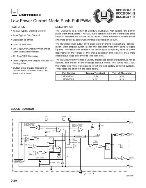
UCC1808-1/-2UCC2808-1/-2UCC3808-1/-204/99FEATURES•130µA Typical Starting Current •1mA Typical Run Current •Operation to 1MHz •Internal Soft Start•On Chip Error Amplifier With 2MHz Gain Bandwidth Product •On Chip VDD Clamping•Dual Output Drive Stages In Push-Pull Configuration•Output Drive Stages Capable Of 500mA Peak Source Current, 1APeak Sink CurrentLow Power Current Mode Push-PullPWMBLOCK DIAGRAMDESCRIPTIONThe UCC3808is a family of BiCMOS push-pull,high-speed,low power,pulse width modulators.The UCC3808contains all of the control and drive circuitry required for off-line or DC-to-DC fixed frequency current-mode switching power supplies with minimal external parts count.The UCC3808dual output drive stages are arranged in a push-pull configu-ration.Both outputs switch at half the oscillator frequency using a toggle flip-flop.The dead time between the two outputs is typically 60ns to 200ns depending on the values of the timing capacitor and resistors,thus limits each output stage duty cycle to less than 50%.The UCC3808family offers a variety of package options temperature rangeoptions,and choice of undervoltage lockout levels.The family has UVLO thresholds and hysteresis options for off-line and battery powered systems.Thresholds are shown in the table below.Part Number Turn on Threshold Turn off Threshold UCCx808-112.5V 8.3V UCCx808-24.3V4.1V2CONNECTION DIAGRAMELECTRICAL CHARACTERISTICS:Unless otherwise specified,T A = 0°C to 70°C for the UCC3808-X, –40°C to 85°C forthe UCC2808-X and –55°C to 125°C for the UCC1808-X,VDD = 10V (Note 6), 1µF capacitor from VDD to GND, R = 22k Ω,C = 330pF. T A =T J .PARAMETER TEST CONDITIONS MIN TYP MAX UNITSOscillator Section Oscillator Frequency 175194213kHz Oscillator Amplitude/VDD (Note 1)0.440.50.56V/V Error Amplifier Section Input Voltage COMP = 2V 1.952 2.05V Input Bias Current –11µA Open Loop Voltage Gain 6080dB COMP Sink Current FB = 2.2V,COMP = 1V 0.3 2.5mA COMP Source Current FB = 1.3V,COMP= 3.5V –0.2–0.5mA PWM SectionMaximum Duty Cycle Measured at OUTA or OUTB 484950%Minimum Duty Cycle COMP = 0V 0%Current Sense Section Gain (Note 2) 1.9 2.2 2.5V/V Maximum Input Signal COMP = 5V (Note 3)0.450.50.55V CS to Output Delay COMP = 3.5V, CS from 0 to 600mV 100200ns CS Source Current –200nA CS Sink Current CS = 0.5V, RC = 5.5V (Note 7)510mA Over Current Threshold 0.70.750.8V COMP to CS Offset CS = 0V 0.350.8 1.2V Output Section OUT Low Level I = 100mA 0.51V OUT High Level I = –50mA,VDD – OUT 0.51VRise Time C L = 1nF2560nsFall Time C L = 1nF 2560ns Undervoltage Lockout Section Start Threshold UCCx808-1 (Note 6)11.512.513.5VUCCx808-2 4.1 4.3 4.5VSupply Voltage (IDD ≤10mA). . . . . . . . . . . . . . . . . . . . . . .15V Supply Current . . . . . . . . . . . . . . . . . . . . . . . . . . . . . . . . .20mA OUTA/OUTB Source Current (peak). . . . . . . . . . . . . . . .–0.5A OUTA/OUTB Sink Current (peak). . . . . . . . . . . . . . . . . . .1.0A Analog Inputs (FB, CS).–0.3V to VDD+0.3V, not to exceed 6V Power Dissipation at T A = 25°C (N Package). . . . . . . . . . . .1W Power Dissipation at T A = 25°C (D Package). . . . . . . .650mW Storage Temperature . . . . . . . . . . . . . . . . . . .–65°C to +150°C Junction Temperature. . . . . . . . . . . . . . . . . . .–55°C to +150°C Lead Temperature (Soldering, 10sec.). . . . . . . . . . . . .+300°CCurrents are positive into, negative out of the specified terminal.Consult Packaging Section of Databook for thermal limitations and considerations of package.ABSOLUTE MAXIMUM RATINGSORDER INFORMATIONELECTRICAL CHARACTERISTICS:Unless otherwise specified,T A= 0°C to 70°C for the UCC3808-X, –40°C to 85°C for the UCC2808-X and –55°C to 125°C for the UCC1808-X,VDD= 10V (Note 6), 1µF capacitor from VDD to GND, R = 22kΩ,C = 330pF. T A=T J.PARAMETER TEST CONDITIONS MIN TYP MAX UNITS Undervoltage Lockout Section (cont.)Minimum Operating Voltage After Start UCCx808-17.68.39VUCCx808-2 3.9 4.1 4.3V Hysteresis UCCx808-1 3.5 4.2 5.1VUCCx808-20.10.20.3V Soft Start SectionCOMP Rise Time FB = 1.8V, Rise from 0.5V to 4V 3.520ms Overall SectionStartup Current VDD< Start Threshold130260µA Operating Supply Current FB = 0V, CS = 0V (Note 5 and 6)12mA VDD Zener Shunt Voltage IDD= 10mA (Note 4)131415VNote 2: Gain is defined by AVVCOMPCS=∆∆, 0V CS0.4V.Note 3: Parameter measured at trip point of latch with FB at 0V.Note 4: Start threshold and Zener Shunt threshold track one another.Note 5: Does not include current in the external oscillator network.Note 6: For UCCx808-1, set VDD above the start threshold before setting at 10V.Note 7: The internal current sink on the CS pin is designed to discharge an external filter capacitor. It is not intended to be a DC sink path.COMP:COMP is the output of the error amplifier and the input of the PWM comparator.The error amplifier in the UCC3808is a true low-output impedance,2MHz opera-tional amplifier.As such,the COMP pin can both source and sink current.However,the error amplifier is internally current limited,so that zero duty cycle can be externally forced by pulling COMP to GND.The UCC3808family features built-in full cycle soft start. Soft start is implemented as a clamp on the maximum COMP voltage.CS:The input to the PWM,peak current,and overcurrent comparators.The overcurrent comparator is only intended for fault sensing.Exceeding the overcurrent threshold will cause a soft start cycle.An in-ternal MOSFET discharges the current sense filter ca-pacitor to improve dynamic performance of the power converter.FB:The inverting input to the error amplifier.For best stability,keep FB lead length as short as possible and FB stray capacitance as small as possible.GND:Reference ground and power ground for all func-tions.Due to high currents,and high frequency operation of the UCC3808,a low impedance circuit board ground plane is highly recommended.OUTA and OUTB:Alternating high current output stages.Both stages are capable of driving the gate of a power MOSFET.Each stage is capable of500mA peak source current, and 1A peak sink current.The output stages switch at half the oscillator frequency, in a push/pull configuration.When the voltage on the RC pin is rising,one of the two outputs is high,but during fall time,both outputs are off.This“dead time”between the two outputs,along with a slower output rise time than fall time,insures that the two outputs can not be on at the same time.This dead time is typically60ns to200ns and depends upon the values of the timing capacitor and re-sistor.The high-current output drivers consist of MOSFET out-put devices,which switch from VDD to GND.Each out-put stage also provides a very low impedance to overshoot and undershoot.This means that in many cases, external schottky clamp diodes are not required. RC:The oscillator programming pin.The UCC3808’s os-cillator tracks VDD and GND internally,so that variations in power supply rails minimally affect frequency stability. Fig. 1 shows the oscillator block diagram.Only two components are required to program the oscil-lator,a resistor(tied to the VDD and RC),and a capaci-tor(tied to the RC and GND).The approximate oscillator frequency is determined by the simple formula:PIN DESCRIPTIONS34f RCOSCILLATOR =141.where frequency is in Hertz,resistance in Ohms,and ca-pacitance in Farads.The recommended range of timing resistors is between 10k Ωand 200k Ωand range of tim-ing capacitors is between 100pF and 1000pF.Timing re-sistors less than 10k Ωshould be avoided.For best performance,keep the timing capacitor lead to GND as short as possible,the timing resistor lead from VDD as short as possible,and the leads between timing components and RC as short as possible.Separate ground and VDD traces to the external timing network are encouraged.VDD:The power input connection for this device.Al-though quiescent VDD current is very low,total supply current will be higher,depending on OUTA and OUTB current,and the programmed oscillator frequency.Total VDD current is the sum of quiescent VDD current and the average OUT current.Knowing the operating fre-quency and the MOSFET gate charge (Qg),average OUT current can be calculated fromI OUT =Qg • F, where F is frequency.To prevent noise problems,bypass VDD to GND with a ceramic capacitor as close to the chip as possible along with an electrolytic capacitor.A 1µF decoupling capacitor is recommended.PIN DESCRIPTIONS (cont.)Figure 1. Block diagram for oscillator.A 200kHz push-pull application circuit with a full wave rec-tifier is shown in Fig.2.The output,V O ,provides 5V at 75W maximum and is electrically isolated from the input.Since the UCC3808is a peak current mode controller the 2N2222A emitter following amplifier (buffers the CT wave-form)provides slope compensation which is necessary for duty ratios greater than 50%.Capacitor decoupling is very important with a single ground IC controller and a 1µF is suggested as close to the IC as possible.The con-troller supply is a series RC for startup,paralleled with a bias winding on the output inductor used in steady state operation.Isolation is provided by an optocoupler with regulation done on the secondary side using the UC3965Precision Reference with Low Offset Error Amplifier.Small signal compensation with tight voltage regulation is achieved using this part on the secondary side.Many choices ex-ist for the output inductor depending on cost,volume,and mechanically strength.Several design options are iron powder,molypermalloy (MPP),or a ferrite core with an air gap as shown here.The main power transformer is a low profile design,EFD size 25,using Magnetics Inc.P material which is a good choice at this frequency and temperature.The input voltage may range from 36V dc to 72V dc.Refer to application note U-170for addi-tion design information.APPLICATION INFORMATIONAPPLICATION INFORMATION (cont.)56UNITRODE CORPORATION7 CONTINENTAL BLVD. • MERRIMACK, NH 03054TEL. (603) 424-2410FAX (603) 424-3460TYPICAL CHARACTERISTIC CURVESDDIMPORTANT NOTICETexas Instruments and its subsidiaries (TI) reserve the right to make changes to their products or to discontinue any product or service without notice, and advise customers to obtain the latest version of relevant information to verify, before placing orders, that information being relied on is current and complete. All products are sold subject to the terms and conditions of sale supplied at the time of order acknowledgement, including those pertaining to warranty, patent infringement, and limitation of liability.TI warrants performance of its semiconductor products to the specifications applicable at the time of sale in accordance with TI’s standard warranty. Testing and other quality control techniques are utilized to the extent TI deems necessary to support this warranty. Specific testing of all parameters of each device is not necessarily performed, except those mandated by government requirements.CERTAIN APPLICATIONS USING SEMICONDUCTOR PRODUCTS MAY INVOLVE POTENTIAL RISKS OF DEATH, PERSONAL INJURY, OR SEVERE PROPERTY OR ENVIRONMENTAL DAMAGE (“CRITICAL APPLICATIONS”). TI SEMICONDUCTOR PRODUCTS ARE NOT DESIGNED, AUTHORIZED, OR WARRANTED TO BE SUITABLE FOR USE IN LIFE-SUPPORT DEVICES OR SYSTEMS OR OTHER CRITICAL APPLICATIONS. INCLUSION OF TI PRODUCTS IN SUCH APPLICATIONS IS UNDERSTOOD TO BE FULLY AT THE CUSTOMER’S RISK.In order to minimize risks associated with the customer’s applications, adequate design and operating safeguards must be provided by the customer to minimize inherent or procedural hazards.TI assumes no liability for applications assistance or customer product design. TI does not warrant or represent that any license, either express or implied, is granted under any patent right, copyright, mask work right, or other intellectual property right of TI covering or relating to any combination, machine, or process in which such semiconductor products or services might be or are used. TI’s publication of information regarding any third party’s products or services does not constitute TI’s approval, warranty or endorsement thereof.Copyright © 1999, Texas Instruments IncorporatedCopyright © Each Manufacturing Company.All Datasheets cannot be modified without permission.This datasheet has been download from :100% Free DataSheet Search Site.Free Download.No Register.Fast Search System.。
变频空调中基于UCC3818的APFC电路设计
变频空调中基于UCC3818的APFC电路设计
丁京柱
【期刊名称】《电子设计应用》
【年(卷),期】2004(000)001
【摘要】本文介绍了较大功率变频空调的一种APFC方案.它应用升压电路,采用平均电流控制,使功率因数达到0.99以上.结果表明,方案具有较高的可靠性.
【总页数】4页(P79-82)
【作者】丁京柱
【作者单位】德州仪器,上海,有限公司
【正文语种】中文
【中图分类】NT7
【相关文献】
1.基于单周期控制的Boost型APFC电路设计及仿真 [J], 韩晓钢;齐铂金
2.基于UCC3818大功率APFC电源设计 [J], 王建飞;付纯菲;
3.恒流源系统中基于临界导通模式的APFC电路设计 [J], 陈华莉;莫磊;曾勇
4.基于UCC28019的高效率APFC电路设计与研究 [J], 李彩凤;杨风;常宇
5.基于隔离式Cuk变换器的APFC电路设计与研究 [J], 李文萱
因版权原因,仅展示原文概要,查看原文内容请购买。
UCC2818 设计文档
ALTERNATE TRANSFER FUNCTIONS - From SEM1500 (Topic 2): Vboost ⋅ Rsense s( f) ⋅ Lboost⋅ Vp
Gps1 ( f) :=
Simplified equation.
s( f) 1+ 2 2 ⋅ Vboost ⋅ Rsense RL⋅ Cout Gps2 ( f) := ⋅ 2 Vp⋅ RL⋅ ( 1 − D) s( f) 1+ + 1 − D Cout ⋅ RL⋅ ( 1 − D) ⋅ Lboost Lboost⋅ Cout
3
Vin_min := 170 ⋅ volt
∆I :=
0.2⋅ 2 ⋅ Pin Vin_min Vin_min⋅ 2 Vboost Vin_min⋅ 2⋅ D ∆I⋅ fs
∆I = 2.028 amp
D := 1 −
D = 0.369
Lboost :=
Lboost = 0.437 mH
Lboost := 0.5⋅ mH
Po
Vboost Po ⋅
2
∆T = 31.028 ms 16⋅ Vboost
Ic_rms :=
η2
Vboost
3⋅ π ⋅ ( 2 ⋅ Vin_min)
−1
Ic_rms = 3.951 amp
????????????????
Boost Current Sense Resistor: Vdynamic := 0.75⋅ volt Rsense := Vdynamic Ip Rsense = 0.068 Ω
Plimit Pin Plimit Pin
kmpl = 115 %
GC0308ApplicationNotesV1.0_0311
GC0308ApplicationNotesV1.0_0311 VGA CMOS Image Sensor GC0308Application Notes2010-02-08GalaxyCore Inc.GC0308 -- VGA CMOS Image Sensor目录?1. 简介 ................................................................................................ 42. Pixel Array 说明 ........................................................................... 43. 系统应用 ........................................................................................ 5?3.1 3.2 3.3 外围连接............................................................................................ 6 应用时序............................................................................................ 6 芯片控制............................................................................................ 7 3.3.1 寄存器复位................................................................................. 7 3.3.2 Standby 模式控制...................................................................... 7 3.3.3 输出使能控制............................................................................. 8 3.3.4 输出 Pin 驱动能力 ..................................................................... 8?4. 芯片功能方面配置 ........................................................................ 9?4.1 4.2 4.3 Pixel Array 控制................................................................................ 9 时钟预分频........................................................................................ 9 输出时序说明及同步信号控制...................................................... 10 4.3.1 输出时序说明........................................................................... 10 4.3.2 同步信号极性控制................................................................... 11 4.4 4.5 4.6 图像窗口设置.................................................................................. 11 Subsample 输出 ............................................................................... 13 Anti_flicker 与 HB,VB 与CLK 的关系。
Differences Between the UCC3813 and the UCC3800 PWM Families
IMPORTANT NOTICETexas Instruments and its subsidiaries (TI) reserve the right to make changes to their products or to discontinue any product or service without notice, and advise customers to obtain the latest version of relevant information to verify, before placing orders, that information being relied on is current and complete. All products are sold subject to the terms and conditions of sale supplied at the time of order acknowledgment, including those pertaining to warranty, patent infringement, and limitation of liability.TI warrants performance of its semiconductor products to the specifications applicable at the time of sale in accordance with TI’s standard warranty. Testing and other quality control techniques are utilized to the extent TI deems necessary to support this warranty. Specific testing of all parameters of each device is not necessarily performed, except those mandated by government requirements.Customers are responsible for their applications using TI components.In order to minimize risks associated with the customer’s applications, adequate design and operating safeguards must be provided by the customer to minimize inherent or procedural hazards.TI assumes no liability for applications assistance or customer product design. TI does not warrant or represent that any license, either express or implied, is granted under any patent right, copyright, mask work right, or other intellectual property right of TI covering or relating to any combination, machine, or process in which such semiconductor products or services might be or are used. TI’s publication of information regarding any third party’s products or services does not constitute TI’s approval, warranty or endorsement thereof.Copyright © 2000, Texas Instruments Incorporated。
- 1、下载文档前请自行甄别文档内容的完整性,平台不提供额外的编辑、内容补充、找答案等附加服务。
- 2、"仅部分预览"的文档,不可在线预览部分如存在完整性等问题,可反馈申请退款(可完整预览的文档不适用该条件!)。
- 3、如文档侵犯您的权益,请联系客服反馈,我们会尽快为您处理(人工客服工作时间:9:00-18:30)。
PR
SPM
IN(S) IN(R)
LVIC
Shunt Resistor
N
VAC-
NSENSE
Control IC
Fig.1 Typical block diagram of PFC SPM® system
An inrush-current prevention circuit is required due to the large DC link capacitance as shown in Fig. 1. The relay of the circuit should be closed after DC link capacitor is charged far enough. PFC SPM®, miniSPM and control IC can share single GND stage. Usually, this GND and the NSENSE terminal of PFC SPM should have the same potential. Large surge voltage is easily produced between P and N terminals by large current switching. To reduce surge voltage it is important to shorten the DC link bus wiring between PFC SPM and DC link capacitor. In addition, good high frequency characteristic capacitor, such as polypropylene film capacitor should be mounted near to P and N terminals as a snubber.
© 2005
Rev. 1.0.1-2012 2
Fairchild Semiconductor – System Engineering Group
PFC SPM® Design Guide
1. System Configurations
Vac N /F R el ay
VTH RTH S R
NTC Thermistor
Over Current Protection (OCP)
[OCP Level1 –PFC SPM®] PFC SPM can protect from over current situation. When OC(over current) situation happens, the PFC SPM stops operating and generates fault out signal during fault-out duration time(set by CFOD). And then after the duration, it works again according to the input command. Its total propagation delay time may depend on outer op-amp speed. We recommend using a low cost slow op-amp solution with fast protection. It is the OCP level2 protection described in next paragraph. [OCP Level2 (SCP) –PFC control IC] By the peak current limit function of PFC control IC, the system is protected from SC(Short Circuit) situation. The recommended current limit of OCP level 2 is higher than that of OCP level 1. It doesn’t generate the fault out signal but its response is very fast. It will protect the system from short circuit situation during the propagation delay time of OCP level1.
3.
Design Example (PFC SPM® DEMO BOARD) ......................................5
Operating conditions of PFC SPM® demo board: .................................................................................. 5 Output capacitance and Inductance design ............................................................................................ 5 Output Voltage Ripple & Output Capacitance ...................................................................................... 5 Inductance & Input Current Ripple ....................................................................................................... 6 Open Loop Response ............................................................................................................................... 6 Current Loop Amplifier .......................................................................................................................... 7 Voltage Loop Amplifier .......................................................................................................................... 7 Control Loop Implementation ................................................................................................................ 8 Current Loop .......................................................................................................................................... 8 Voltage Loop ......................................................................................................................................... 10 Other Parameters ................................................................................................................................. 10 Over Current Protection....................................................................................................................... 12 Over Voltage Protection ....................................................................................................................... 13 DC-link Voltage Control ...............................................................................................................Circuits
Following Fig. 2 shows the timing chart of protection function. There are two kind of protection level for both OCP and OVP. Generally, PFC control ICs have its own OCP and OVP function. Also, user can make the PFC SPM® stop and output the FO signal under preset OC, OV condition using its Csc input.