TP4366同步四灯显1A移动电源方案_TP4366规格书_TP4366 PDF
AK4366VTP中文资料
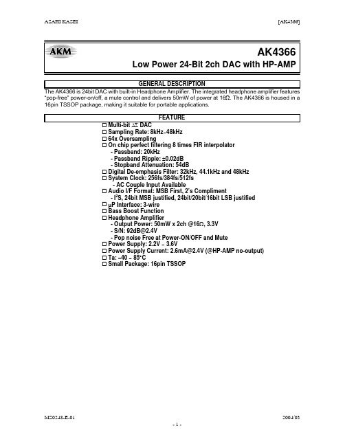
ASAHI KASEI[AK4366]AK4366Low Power 24-Bit 2ch DAC with HP-AMPGENERAL DESCRIPTION The AK4366 is 24bit DAC with built-in Headphone Amplifier. The integrated headphone amplifier features “pop-free” power-on/off, a mute control and delivers 50mW of power at 16Ω. The AK4366 is housed in a 16pin TSSOP package, making it suitable for portable applications. FEATURE Multi-bit ∆Σ DAC Sampling Rate: 8kHz∼48kHz 64x Oversampling On chip perfect filtering 8 times FIR interpolator - Passband: 20kHz - Passband Ripple: ±0.02dB - Stopband Attenuation: 54dB Digital De-emphasis Filter: 32kHz, 44.1kHz and 48kHz System Clock: 256fs/384fs/512fs - AC Couple Input Available Audio I/F Format: MSB First, 2’s Compliment - I2S, 24bit MSB justified, 24bit/20bit/16bit LSB justified µP Interface: 3-wire Bass Boost Function Headphone Amplifier - Output Power: 50mW x 2ch @16Ω, 3.3V - S/N: 92dB@2.4V - Pop noise Free at Power-ON/OFF and Mute Power Supply: 2.2V ∼ 3.6V Power Supply Current: 2.6mA@2.4V (@HP-AMP no-output) Ta: −40 ∼ 85°C Small Package: 16pin TSSOPMS0248-E-01 -1-2004/03ASAHI KASEI[AK4366]MCLKVDDBICK LRCK SDATAAudio InterfaceClock Divider VCOM DAC(Lch)VCOMHDP AmpMUTEHPLATT & Bass BoostDEM & Digital Filter DAC(Rch)HDP AmpMUTEHPRPDN P/S DIF0/CSN DEM/CCLK MUTEN /CDTI VSS Serial I/F HVDD MUTETFigure 1. AK4366 Block DiagramMS0248-E-01 -2-2004/03ASAHI KASEI[AK4366]Ordering GuideAK4366VT AKD4366 −40 ∼ +85°C 16pin TSSOP (0.65mm pitch) Evaluation board for AK4366Pin LayoutMUTEN/CDTI DEM/CCLK DIF0/CSN SDATA LRCK BICK MCLK PDN1 2 3 4 5 6 7 8 Top View16 15 14 13 12 11 10 9HPL HPR HVDD VSS VDD MUTET VCOM P/SMS0248-E-01 -3-2004/03ASAHI KASEI[AK4366]PIN/FUNCTIONNo. 1 Pin Name MUTEN CDTI 2 DEM CCLK 3 4 5 6 7 8 9 10 11 12 13 14 15 16 DIF0 CSN SDATA LRCK BICK MCLK PDN P/S VCOM MUTET VDD VSS HVDD HPR HPL I/O I I I I I I I I I I I I O O O O Function Headphone Amp Mute Pin (P/S pin = “H”) “H”: Normal operation, “L”: Mute Control Data Input Pin (P/S pin = “L”) De-emphasis Pin (P/S pin = “H”) “H”: ON(44.1kHz), “L”: OFF Control Data Clock Pin (P/S pin = “L”) Audio Interface Format Pin (P/S pin = “H”) “H”: I2S, “L”: 24bit MSB justified Control Data Chip Select Pin (P/S pin = “L”) Audio Serial Data Input Pin L/R Clock Pin This clock determines which audio channel is currently being input on SDATA pin. Serial Bit Clock Pin This clock is used to latch audio data. Master Clock Input Pin Power-down & Reset Pin When at “L”, the AK4366 is in power-down mode and is held in reset. The AK4366 should always be reset upon power-up. Control Mode Select Pin (Internal Pull-down Pin) “H”: Parallel, “L”: 3-wire Serial Common Voltage Output Pin Normally connected to VSS pin with 0.1µF ceramic capacitor in parallel with a 2.2µF electrolytic capacitor. Mute Time Constant Control Pin Connected to VSS pin with a capacitor for mute time constant. Power Supply Pin Ground Pin Power Supply Pin for Headphone Amp Rch Headphone Amp Output Pin Lch Headphone Amp Output PinNote: All digital input pins except internal pull-down pin must not be left floating.Handling of Unused PinThe unused I/O pins should be processed appropriately as below. Classification Analog Digital Pin Name MUTET, HPR, HPL DEM, DIF0 Setting These pins should be open. These pins should be connected to VSS.MS0248-E-01 -4-2004/03ASAHI KASEI[AK4366]ABSOLUATE MAXIMUM RATING (VSS=0V; Note 1) Parameter Symbol min Power Supplies Analog, Digital VDD −0.3 HP-AMP HVDD −0.3 Input Current (any pins except for supplies) IIN Input Voltage VIN −0.3 Ambient Temperature Ta −40 Storage Temperature Tstg −65 Note 1. All voltages with respect to ground.max 4.6 4.6 ±10 VDD+0.3 or 4.6 85 150Units V V mA V °C °CWARNING: Operation at or beyond these limits may result in permanent damage to the device. Normal operation is not guaranteed at these extremes.RECOMMEND OPERATING CONDITIONS (VSS=0V; Note 1) Parameter Symbol min typ Power Supplies Analog, Digital VDD 2.2 2.4 (Note 2) HP-AMP HVDD 2.2 2.4 Note 1. All voltages with respect to ground. Note 2. VDD should be same voltage as HVDD.* AKM assumes no responsibility for usage beyond the conditions in this datasheet.max 3.6 3.6Units V VMS0248-E-01 -5-2004/03ASAHI KASEI[AK4366]ANALOG CHARACTERISTICS (Ta=25°C; VDD=HVDD=2.4V, VSS=0V; fs=44.1kHz; BOOST OFF; Signal Frequency =1kHz; Measurement band width=10Hz ∼ 20kHz; Load impedance is a serial connection with RL =16Ω and CL=220µF. (Refer to Figure 19); unless otherwise specified) Parameter min typ max Units 24 bit DAC Resolution Headphone-Amp: (HPL/HPR pins) (Note 3) Analog Output Characteristics THD+N (−4.8dBFS Output, Po=10mW@16Ω, 2.4V) dB −55 −45 dB (−3dBFS Output, Po=28mW@16Ω, 3.3V) −55 dB (−3dBFS Output, Po=14mW@32Ω, 3.3V) −57 D-Range (−60dBFS Output, A-weighted, 2.4V) 84 92 dB 94 dB (−60dBFS Output, A-weighted, 3.3V) S/N (A-weighted, 2.4V) 84 92 dB (A-weighted, 3.3V) 94 dB Interchannel Isolation 60 80 dB DC Accuracy Interchannel Gain Mismatch 0.2 dB Gain Drift 200 ppm/°C Load Resistance (Note 4) 16 Ω Load Capacitance 300 pF Output Voltage (Note 5) 1.02 1.13 1.24 Vpp (−4.8dBFS Output) Max Output Power 26 mW (RL=16Ω, 2.4V) 50 mW (RL=16Ω, 3.3V) Power Supplies Power Supply Current Normal Operation (PDN pin = “H”) (Note 6) VDD 1.6 2.8 mA HVDD 1.0 2.0 mA Power-Down Mode (PDN pin = “L”) (Note 7) 1 100 µA Note 3. DACL=DACR= “1”, ATTL=ATTR=0dB. Note 4. AC Load Note 5. Output voltage is proportional to VDD voltage. Vout = 0.47 x VDD(typ)@−4.8dBFS. Note 6. PMDAC=PMHPL=PMHPR= “1”, MUTEN= “1” and HP-Amp output is off. Note 7. All digital input pins including clock pins (MCLK, BICK and LRCK) are held at VSS.MS0248-E-01 -6-2004/03ASAHI KASEI[AK4366]FILTER CHARACTERISTICS (Ta=25°C; VDD, HVDD=2.2 ∼ 3.6V; fs=44.1kHz; De-emphasis = “OFF”) Parameter Symbol min typ max Units DAC Digital Filter: (Note 8) Passband PB 0 20.0 kHz −0.05dB (Note 9) 22.05 kHz −6.0dB Stopband (Note 9) SB 24.1 kHz Passband Ripple PR dB ±0.02 Stopband Attenuation SA 54 dB Group Delay (Note 10) GD 20.8 1/fs Group Delay Distortion 0 µs ∆GD DAC Digital Filter + Analog Filter: (Note 8) (Note 11) Frequency Response FR dB 0 ∼ 20.0kHz ±0.5 BOOST Filter: (Note 11) (Note 12) Frequency Response 20Hz FR dB 5.76 MIN 100Hz dB 2.92 1kHz dB 0.02 20Hz FR dB 10.80 MID 100Hz dB 6.84 1kHz dB 0.13 20Hz FR dB 16.06 MAX 100Hz dB 10.54 1kHz dB 0.37 Note 8. BOOST OFF (BST1-0 bit = “00”) Note 9. The passband and stopband frequencies scale with fs. For example, PB=0.4535*fs(@±0.05dB), SB=0.546*fs(@−54dB). Note 10. This is the calculated delay time caused by digital filtering. This time is measured from the setting of the 24bit data of both channels to the input registers to the output of the analog signal. Note 11. DAC HPL, HPR Note 12. These frequency responses scale with fs. If high-level signal is input, the AK4366 clips at low frequency.Boost Filter (fs=44.1kHz) 20 15 Level [dB] MID 10 MIN 5 0 -5 10 100 Frequency [Hz] 1000 10000MAXFigure 2. Boost Frequency (fs=44.1kHz)MS0248-E-01 -7-2004/03ASAHI KASEI[AK4366]DC CHARACTERISTICS (Ta=25°C; VDD, HVDD=2.2 ∼ 3.6V) Parameter Symbol min High-Level Input Voltage VIH 70%DVDD Low-Level Input Voltage VIL Input Voltage at AC Coupling (Note 13) VAC 1.0 Input Leakage Current (Note 14) Iin Note 13. Only MCLK pin. (Figure 19) Note 14. P/S pin has internal pull-down device, nominally 100kΩ.typ -max 30%DVDD ±10Units V V Vpp µASWITCHING CHARACTERISTICS(Ta=25°C; VDD, HVDD=2.2 ∼ 3.6V) Parameter Symbol min typ max Units Master Clock Timing Frequency fCLK 2.048 24.576 MHz Pulse Width Low (Note 15) tCLKL 0.4/fCLK ns Pulse Width High (Note 15) tCLKH 0.4/fCLK ns AC Pulse Width (Note 18) tACW 20 ns LRCK Timing Frequency fs 8 44.1 48 kHz Duty Cycle: Duty 45 55 % Serial Interface Timing (Note 16) BICK Period tBCK 1/(64fs) ns BICK Pulse Width Low tBCKL 130 ns Pulse Width High tBCKH 130 ns (Note 17) tLRB 50 ns LRCK Edge to BICK “↑” (Note 17) tBLR 50 ns BICK “↑” to LRCK Edge SDATA Hold Time tSDH 50 ns SDATA Setup Time tSDS 50 ns Control Interface Timing CCLK Period tCCK 200 ns CCLK Pulse Width Low tCCKL 80 ns Pulse Width High tCCKH 80 ns CDTI Setup Time tCDS 40 ns CDTI Hold Time tCDH 40 ns CSN “H” Time tCSW 150 ns tCSS 50 ns CSN “↑” to CCLK “↑” tCSH 50 ns CCLK “↑” to CSN “↑” Note 15. Except AC coupling. Note 16. Refer to “Serial Data Interface”. Note 17. BICK rising edge must not occur at the same time as LRCK edge. Note 18. Pulse width to ground level when MCLK is connected to a capacitor in series and a resistor is connected to ground. (Refer to Figure 3.)MS0248-E-01 -8-2004/03ASAHI KASEI[AK4366]Timing Diagram1/fCLK1000pF MCLK Input 100kΩ VSS Measurement PointtACWtACWVAC VSSFigure 3. MCLK AC Coupling Timing1/fCLK VIH VIL tCLKH tCLKLMCLK1/fs VIH VILLRCKtBCK VIH VIL tBCKH tBCKLBICKFigure 4. Clock TimingLRCK tBLR tLRBVIH VILBICK tSDS tSDHVIH VILSDATAVIH VILFigure 5. Serial Interface Timing MS0248-E-01 -92004/03ASAHI KASEI[AK4366]VIH CSN VIL tCSS tCCKL tCCKH VIH VIL tCDS tCDH VIH VILCCLKCDTIC1C0R/WA4Figure 6. WRITE Command Input TimingtCSW VIH CSN VIL tCSH CCLK VIH VILCDTID3D2D1D0VIH VILFigure 7. WRITE Data Input TimingtPDPDNVILFigure 8. Power-down & Reset TimingMS0248-E-01 - 10 -2004/03OPERATION OVERVIEWSystem ClockThe external clocks required to operate the AK4366 are MCLK(256fs/384fs/512fs), LRCK(fs) and BICK. The masterclock (MCLK) should be synchronized with sampling clock (LRCK). The phase between these clocks does not matter.The frequency of MCLK is detected automatically, and the internal master clock becomes the appropriate frequency.Table 1 shows system clock example.LRCK MCLK (MHz) BICK (MHz)fs 256fs 384fs 512fs 64fs8kHz 2.048 3.072 4.096 0.51211.025kHz 2.8224 4.2336 5.6448 0.705612kHz 3.072 4.608 6.144 0.76816kHz 4.096 6.144 8.192 1.02422.05kHz 5.6448 8.4672 11.2896 1.411224kHz 6.144 9.216 12.288 1.53632kHz 8.192 12.288 16.384 2.04844.1kHz 11.2896 16.9344 22.5792 2.822448kHz 12.288 18.432 24.576 3.072Table 1. System Clock ExampleIn serial mode (P/S pin = “L”), all external clocks (MCLK, BICK and LRCK) should always be present whenever theDAC is in normal operation mode (PMDAC bit = “1”). If these clocks are not provided, the AK4366 may draw excesscurrent and will not operate properly because it utilizes these clocks for internal dynamic refresh of registers. If theexternal clocks are not present, the DAC should be placed in power-down mode (PMDAC bit = “0”). When MCLK isinput with AC coupling, the MCKAC bit should be set to “1”.In parallel mode (P/S pin = “H”), all external clocks (MCLK, BICK and LRCK) should always be present whenever theDAC is in normal operation mode (PDN pin = “H”). If these clocks are not provided, the AK4366 may draw excesscurrent and will not operate properly because it utilizes these clocks for internal dynamic refresh of registers. If theexternal clocks are not present, the DAC should be placed in power-down mode (PDN pin = “L”).For low sampling rates, DR and S/N degrade because of the outband noise. In serial mode (P/S pin = “L”), DR and S/Nare improved by setting DFS1 bit to “1”. Table 2 shows S/N of HP-amp output. When the DFS1 bit is “1”, MCLK needs512fs.S/N (fs=8kHz, A-weighted) DFS1 DFS0 Over Sample Rate fs MCLK HP-amp0 0 64fs 8kHz ∼48kHz256fs/384fs/512fs 56dB Default 0 1 128fs 8kHz ∼24kHz256fs/384fs/512fs 75dB 1 x 256fs 8kHz ∼12kHz512fs 92dB Table 2. Relationship among fs, MCLK frequency and S/N of HP-ampSerial Data InterfaceThe AK4366 interfaces with external system via the SDATA, BICK and LRCK pins. In serial mode (P/S pin = “L”), fivedata formats are available and are selected by setting DIF2, DIF1 and DIF0 bits (Table 3). In parallel mode (P/S pin =“H”), two data formats are available and are selected by setting DIF0 pin (Table 3). Mode 0 is compatible with existing16bit DACs and digital filters. Mode 1 is a 20bit version of Mode 0. Mode 4 is a 24bit version of Mode 0. Mode 2 issimilar to AKM ADCs and many DSP serial ports. Mode 3 is compatible with the I 2S serial data protocol. In Modes 2 and3 with BICK ≥48fs, the following formats are also valid: 16-bit data followed by eight zeros (17th to 24th bits) and 20-bitdata followed by four zeros (21st to 24th bits). In all modes, the serial data is MSB first and 2’s complement format.DIF2 bit DIF1 bit DIF0 bit MODE BICK Figure0 0 0 0: 16bit, LSB justified 32fs ≤ BICK ≤ 64fsFigure 90 0 1 1: 20bit, LSB justified 40fs ≤ BICK ≤ 64fs Figure 100 1 0 2: 24bit, MSB justified 48fs ≤ BICK ≤ 64fsFigure 110 1 1 3: I 2S Compatible BICK=32fs or 48fs ≤ BICK ≤ 64fs Figure 121 0 0 4: 24bit, LSB justified 48fs ≤ BICK ≤ 64fsFigure 10Table 3. Audio Data Format (Serial Mode)DIF0 pin MODE BICK FigureL 2: 24bit, MSB justified 48fs ≤ BICK ≤ 64fs Figure 11 H 3: I 2S Compatible BICK=32fs or 48fs ≤ BICK ≤ 64fs Figure 12Table 4. Audio Data Format (Parallel Mode)SDATABICKLRCKSDATABICK(32fs)Mode 0Mode 0Figure 9. Mode 0 TimingSDATALRCKBICKMode 1SDATAMode 4Figure 10. Mode 1, 4 TimingLRCK BICKSDATA16bitSDATA20bitSDATA24bitFigure 11. Mode 2 TimingLRCKBICKSDATA16bitSDATA20bitSDATA24bitBICK(32fs)SDATA16bitFigure 12. Mode 3 TimingDigital AttenuatorThe AK4366 has a channel-independent digital attenuator (256 levels, 0.5dB step). This digital attenuator is placed before the D/A converter. ATTL/R7-0 bits set the attenuation level (0dB to −127dB or MUTE) for each channel (Table 5). At DATTC bit = “1”, ATTL7-0 bits control both Lch and Rch attenuation levels. At DATTC bit = “0”, ATTL7-0 bits control the Lch level and ATTR7-0 bits control the Rch level. In parallel mode (P/S pin = “H”), digital attenuator is fixed to 0dB. When HPM bit = “1”, (L+R)/2 summation is done after volume control.ATTL7-0AttenuationATTR7-0FFH 0dBFEH −0.5dBFDH −1.0dBFCH −1.5dB: :: :02H −126.5dB01H −127.0dB00H MUTE (−∞) DefaultTable 5. Digital Volume ATT valuesThe ATS bit sets the transition time between set values of ATT7-0 bits as either 1061/fs or 7424/fs (Table 6). When ATS bit = “0”, a soft transition between the set values occurs(1062 levels). It takes 1061/fs (24ms@fs=44.1kHz) from FFH(0dB) to 00H(MUTE). The ATTs are 00H when the PMDAC bit is “0”. When the PMDAC returns to “1”, the ATTs fade to their current value. Digital attenuator is independent of the soft mute function.ATT speedATS0dB to MUTE 1 stepDefault0 1061/fs 4/fs1 7424/fs 29/fsTable 6. Transition time between set values of ATT7-0 bitsSoft MuteSoft mute operation is performed at digital domain. In serial mode (P/S pin = “L”), when the SMUTE bit goes to “1”, the output signal is attenuated by −∞ during ATT_DATA×ATT transition time (Table 6) from the current ATT level. When the SMUTE bit is returned to “0”, the mute is cancelled and the output attenuation gradually changes to the ATT level during ATT_DATA×ATT transition time. If the soft mute is cancelled before attenuating to −∞ after starting the operation, the attenuation is discontinued and returned to ATT level by the same cycle. The soft mute is effective for changing the signal source without stopping the signal transmission. In parallel mode (P/S pin = “H”), soft mute is not available.Attenuation-∞Analog OutputFigure 13. Soft Mute FunctionNotes:(1) ATT_DATA×ATT transition time (Table 6). For example, this time is 3712LRCK cycles (3712/fs) at ATS bit =“1” and ATT_DATA = “128”.(2) The analog output corresponding to the digital input has a group delay, GD.(3) If the soft mute is cancelled before attenuating to −∞ after starting the operation, the attenuation is discontinuedand returned to ATT level by the same cycle.De-emphasis FilterThe AK4366 includes a digital de-emphasis filter (tc = 50/15µs) by IIR filter corresponding to three sampling frequencies (32kHz, 44.1kHz and 48kHz). In serial mode (P/S pin = “L”), the de-emphasis filter is enabled by setting DEM1-0 bits (Table 7).DEM1 bit DEM0 bit De-emphasis0 044.1kHzDefault0 1 OFF48kHz1 01 132kHzTable 7. De-emphasis Filter Frequency Select (Serial Mode)In parallel mode (P/S pin = “H”), the de-emphasis filter corresponding to 44.1kHz is enabled by setting DEM pin “H” (Table 8).DEM pin De-emphasisL OFFH 44.1kHzTable 8. De-emphasis Filter Frequency Select (Parallel Mode)Bass Boost FunctionIn serial mode (P/S pin = “L”), the low frequency boost signal can be output from DAC by controlling BST1-0 bits (Table 9). The setting value is common in Lch and Rch.BST1 bit BST0 bit BOOSTDefault0 0 OFF0 1 MIN1 0 MID1 1 MAXTable 9. Low Frequency Boost SelectSystem ResetThe AK4366 should be reset once by bringing PDN “L” upon power-up.In serial mode (P/S pin = “L”), after exiting reset, VCOM, DAC, HPL and HPR switch to the power-down state. The contents of the control register are maintained until the reset is done. DAC exits reset and power down state by MCLK after PMDAC bit is changed to “1”, and then DAC is powered up and the internal timing starts clocking by LRCK “↑”. DAC is in power-down mode until MCLK and LRCK are input.In parallel mode (P/S pin = “H”), VCOM and DAC are powered up by PDN pin “H”. Headphone amp is powered up by MUTEN pin “H”. DAC exits reset and power down state by MCLK after PDN pin goes to “H”, and then DAC is powered up and the internal timing starts clocking by LRCK “↑”. DAC is in power-down mode until MCLK and LRCK are input.Headphone OutputPower supply voltage for the Headphone-amp is supplied from the HVDD pin and centered on the 0.45 x VDD voltage.The Headphone-amp output load resistance is min.16Ω.1) Parallel mode (P/S pin = “H”)When MUTEN pin is set to “H” at PDN pin = “H”, common voltage goes to 0.45 x VDD. When MUTEN pin is set to “L”,common voltage goes to VSS, and the outputs (HPL and HPR pins) are VSS. When PDN pin is “L”, headphoneamplifiers are powered-down perfectly, and the outputs (HPL and HPR pins) are VSS.2) Serial mode (P/S pin = “L”)When the MUTEN bit is “1” at PMHPL=PMHPR= “1”, the common voltage rises to 0.45 x VDD. When the MUTEN bitis “0”, the common voltage of Headphone-amp falls and the outputs (HPL and HPR pins) go to VSS. When PMHPL andPMHPR bits are “0”, the Headphone-amps are powered-down perfectly, and the outputs (HPL and HPR pins) are VSS.A capacitor between the MUTET pin and ground reduces pop noise at power-up/down. It isrecommended that the capacitor with small variation of capacitance and low ESR (Equivalent SeriesResistance) over all temperature range, since the rise and fall time in Table 10 depend on thecapacitance and ESR of the external capacitor at MUTET pin.t r : Rise Time up to VCOM/2 100k x C (typ)t f : Fall Time down to 0V 200k x C (typ)Table 10. Headphone-Amp Rise/Fall Time[Example] : A capacitor between the MUTET pin and ground = 1.0µF:Time constant of rise time: t r = 100k Ω x 1µF = 100ms(typ)Time constant of fall time: t f = 200k Ω x 1µF = 200ms(typ)MUTEN bitPMHPL/R bitHPL/R pin (1) (2)(4)(3)t r t fVCOM/2VCOMFigure 14. Power-up/Power-down Timing for Headphone-amp(1) Headphone-amp power-up (PMHPL and PMHPR bits = “1”). The outputs are still VSS.(2) Headphone-amp common voltage rise up (MUTEN bit = “1”). Common voltage of Headphone-amp is rising. This risetime depends on the capacitor value connected with the MUTET pin. The rise time up to VCOM/2 is t r = 100k x C(typ)when the capacitor value on MUTET pin is “C”.(3) Headphone-amp common voltage fall down (MUTEN bit = “0”). Common voltage of Headphone-amp is falling toVSS. This fall time depends on the capacitor value connected with the MUTET pin. The fall time down to 0V is t f =200k x C(typ) when the capacitor value on MUTET pin is “C”.(4) Headphone-amp power-down (PMHPL, PMHPR bits = “0”). The outputs are VSS. If the power supply is switched offor Headphone-amp is powered-down before the common voltage goes to VSS, some pop noise occurs.The cut-off frequency of Headphone-amp output depends on the external resistor and capacitor used. Table 11 shows thecut off frequency and the output power for various resistor/capacitor combinations. The headphone impedance R L is 16Ω.Output powers are shown at HVDD = 2.4, 3.0 and 3.3V. The output voltage of headphone is 0.47 x VDD (Vpp)@−4.8dBFS.Figure 15. External Circuit Example of HeadphoneOutput Power [mW] R [Ω] C [µF]fc [Hz] BOOST=OFF fc [Hz] BOOST=MIN 2.4V 3.0V 3.3V 220 45 17 0100 100 43 15 24 28 100 70 28 6.847 149 78 7 12 14 100 50 19 16 47 106 474 6 7 Table 11. Relationship of external circuit, output power and frequency responsePower-Up/Down Sequence1) Parallel mode (P/S pin = “H”)Power SupplyPDN pinClock InputSDTI pinDAC Internal StateHPL/R pin MUTEN pinFigure 16. Power-up/down sequence of DAC and HP-amp(1) PDN pin should be set to “H” at least 150ns after the power is supplied.(2) External clocks (MCLK, BICK, LRCK) are needed to operate DAC. When PDN pin = “L”, these clocks can bestopped. Headphone amp can operate without these clocks.(3) MUTEN pin should be set to “H” at least 2ms after PDN pin goes to “H”.(4) Rise time of headphone amp is determined by external capacitor (C) of MUTET pin. The rise time up to VCOM/2 ist r = 100k x C(typ). When C=1µF, time constant is 100ms(typ).(5) Fall time of headphone amp is determined by external capacitor (C) of MUTET pin. The fall time down to 0V is t f =200k x C(typ). When C=1µF, time constant is 200ms(typ).PDN pin should be set to “L” after HPL and HPR pins go to VSS.(6) Analog output corresponding to digital input has the group delay (GD) of 20.8/fs (=472µs@fs=44.1kHz).(7) Power supply should be switched off after headphone amp is powered down (HPL/R pins become “L”).2) Serial mode (P/S pin = “L”)Power Supply PDN pinPMVCM bitClock InputSDTI pin PMDAC bit DAC Internal State HPL/R pinPMHPL, PMHPR bit ATTL7-0 ATTR7-0 bitMUTEN bitDACL, DACR bitFigure 17. Power-up/down sequence of DAC and HP-amp(1) PDN pin should be set to “H” at least 150ns after the power is supplied.(2) PMVCM and PMDAC bits should be changed to “1” after PDN pin goes to “H”.(3) External clocks (MCLK, BICK, LRCK) are needed to operate DAC. When PMDAC bit = “0”, these clocks can bestopped. Headphone amp can operate without these clocks.(4) DACL and DACR bits should be changed to “1” after PMDAC bit is changed to “1”.(5) PMHPL, PMHPR and MUTEN bits should be changed to “1” at least 2ms (in case external capacitance at VCOM pinis 2.2µF) after DACL and DACR bits are changed to “1”.(6) Rise time of headphone amp is determined by external capacitor (C) of MUTET pin. The rise time up to VCOM/2 ist r = 100k x C(typ). When C=1µF, time constant is 100ms(typ).(7) Fall time of headphone amp is determined by external capacitor (C) of MUTET pin. The fall time down to 0V is t f =200k x C(typ). When C=1µF, time constant is 200ms(typ).PMHPL, PMHPR, DACL and DACR bits should be changed to “0” after HPL and HPR pins go to VSS. (8) Analog output corresponding to digital input has the group delay (GD) of 20.8/fs(=472µs@fs=44.1kHz). (9) ATS bit sets transition time of digital attenuator. Default value is 1061/fs(=24ms@fs=44.1kHz).(10) Power supply should be switched off after headphone amp is powered down (HPL/R pins become “L”).Mode Control InterfaceSome function of AK4366 can be controlled by both pins (parallel control mode) and register (serial control mode) shown in Table 12. The serial control interface is enabled by the P/S pin = “L”. Internal registers may be written by 3-wire µP interface pins: CSN, CCLK and CDTI. The data on this interface consists of Chip Address (2bits, fixed to “01”), Read/Write (1bit; fixed to “1”, Write only), Register Address (MSB first, 5bits) and Control Data (MSB first, 8bits). AK4366 latches the data on the rising edge of CCLK, so data should clocked in on the falling edge. The writing of data becomes valid by 16th CCLK “↑”. The clock speed of CCLK is 5MHz (max).Function Parallel mode Serial mode De-emphasis 44.1kHz 32kHz/44.1kHz/48kHz SMUTE Not Available Available Audio I/F Format I2S, Left justified I2S, Left Justified, Right justified Digital Attenuator Not Available Available Bass Boost Not Available Available Power Management Not Available AvailableDefault State at PDN pin = “L” → “H”Power up Power downTable 12. Function ListPDN pin = “L” resets the registers to their default values. When the state of P/S pin is changed, AK4366 should be reset by PDN pin = “L”.CDTICCLKCSNC1-C0:Chip Address (Fixed to “01”)R/W: READ/WRITE (Fixed to “1”, Write only) A4-A0:Register Address D7-D0:Control DataFigure 18. 3-wire Serial Control I/F TimingRegister MapRegisterName D7 D6 D5 D4 D3 D2 D1 D0 AddrManagement 0 0 000HPowerMUTEN PMHPR PMHPL PMDAC PMVCM01H Mode Control 0 0 MCKAC HPM DIF2 DIF1 DIF0 DFS1 DFS01 0 0 0Control02HModeSMUTE BST1 BST0 DEM1 DEM02 0 0 0 0 ATSControl03HModeDATTC BCKP LRP 04H DAC Lch ATT ATTL7ATTL6ATTL5ATTL4ATTL3ATTL2 ATTL1 ATTL005H DAC Rch ATT ATTR7ATTR6ATTR5ATTR4ATTR3ATTR2 ATTR1 ATTR0DACRDACL Output06HSelect 0 0 0 0 0 0All registers inhibit writing at PDN pin = “L”.PDN pin = “L” resets the registers to their default values.For addresses from 07H to 1FH, data must not be written.Register DefinitionsName D7 D6 D5 D4 D3 D2 D1 D0 RegisterAddrPowerManagement 0 0 000HMUTEN PMHPR PMHPL PMDAC PMVCM Default 0 0 0 0 0 0 0 0PMVCM: Power Management for VCOM Block0: Power OFF (Default)1: Power ONIn parallel mode (P/S pin = “H”), PMVCM bit is fixed to “1”.PMDAC: Power Management for DAC Blocks0: Power OFF (Default)1: Power ONWhen PMDAC bit is changed from “0” to “1”, DAC is powered-up to the current register values (ATTvalue, sampling rate, etc). In parallel mode (P/S pin = “H”), PMDAC bit is fixed to “1”.PMHPL: Power Management for Lch of Headphone Amp0: Power OFF (Default). HPL pin becomes VSS (0V).1: Power ONPMHPR: Power Management for Rch of Headphone Amp0: Power OFF (Default). HPR pin becomes VSS (0V).1: Power ONMUTEN: Headphone Amp Mute Control0: Mute (Default). HPL and HPR pins go to VSS(0V).1: Normal operation. HPL and HPR pins go to 0.45 x VDD.All blocks can be powered-down by setting the PDN pin to “L” regardless of register values setup. All blocks can be also powered-down by setting all bits of this address to “0”. In this case, control register values are maintained.01H Mode Control 0 0 MCKAC HPM DIF2 DIF1 DIF0 DFS1 DFS0 Default 0 0 0 0 1 0 0 0 DFS1-0: Oversampling Speed Select (Table 2)Default: “00” (64fs)DIF2-0: Audio Data Interface Format Select (Table 3)Default: “010” (Mode 2)HPM: Mono Output Select of Headphone0: Normal Operation (Default)1: Mono. (L+R)/2 signals from the DAC are output to both Lch and Rch of headphone.MCKAC: MCLK Input Mode Select0: CMOS input (Default)1: AC coupling inputName D7 D6 D5 D4 D3 D2 D1 D0 RegisterAddr1 0 0 0ControlMode02HSMUTE BST1 BST0 DEM1 DEM0 Default 0 0 0 0 0 0 0 1 DEM1-0: De-emphasis Filter Frequency Select (Table 7)Default: “01” (OFF)BST1-0: Low Frequency Boost Function Select (Table 9)Default: “00” (OFF)SMUTE: Soft Mute Control0: Normal operation (Default)1: DAC outputs soft-muted。
TP4313_DB1_V1.0
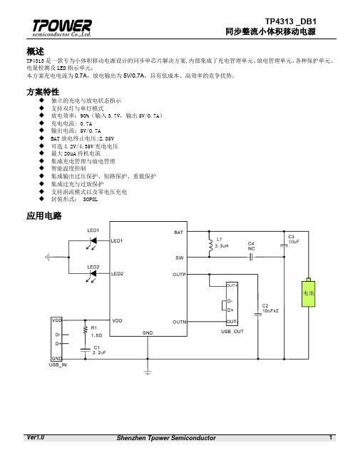
概述TP4313是一款专为小体积移动电源设计的同步单芯片解决方案,内部集成了充电管理单元、放电管理单元、各种保护单元、电量检测及LED指示单元;本方案充电电流为0.7A,放电输出为5V/0.7A,具有低成本、高效率的竞争优势。
方案特性◆独立的充电与放电状态指示◆支持双灯与单灯模式◆放电效率:90%(输入3.7V,输出5V/0.7A)◆充电电流: 0.7A◆输出电流:5V/0.7A◆BAT放电终止电压:2.85V◆可选4.2V/4.35V充电电压◆最大20uA待机电流◆集成充电管理与放电管理◆智能温度控制◆集成输出过压保护、短路保护、重载保护◆集成过充与过放保护◆支持涓流模式以及零电压充电◆封装形式: SOP8L应用电路芯片管脚ESOP8L应用关键点1、 5V输出端的USB外壳不能接GND,需浮空;2、电阻R1对封装无要求,但是R1不能省略;3、输出D+/D-若不加分压电阻则需要短接,否则对某些品牌手机不能充电(比如苹果);如果加分压电阻,则需保证分压电阻的总等效电阻至少为OUTN等效电阻的6倍以上,否则插入负载时不能自动识别;OUTN默认电阻为50K,可以在OUTN于GND并联电阻以减小OUTN的总等效电阻;4、输出电容C2选择低ESR的贴片电容,否则会影响输出纹波;5、电感L1的饱和电流需大于2.5A,否则因电感饱和可能会导致芯片工作不正常;6、 TP4313集成了过充保护、过放保护、过温保护、输出过压保护、输出重载保护、输出短路保护等多重保护机制,也可以额外再加一颗DW01对系统进行双重保护;7、充电时,LED1以1Hz频率闪烁,电池充饱后LED1常亮;放电时,LED2常亮,放电结束后LED2熄灭;8、对于可以用一颗LED灯的模具,TP4313也可以只用一颗LED同时实现充电与放电指示,只需将芯片的LED1与LED2短接后再接LED灯,充电放电指示方式与以上一样,只是用同一颗灯实现而已。
PCB设计参考1、5V输出端的USB外壳不能接GND,需浮空;2、整个PCB建议敷铜散热,散热面积尽量大;3、BAT与地的电容C3靠近IC的BAT 和GND脚,BAT+和BAT-需先经过BAT电容再到IC,各GND走线要尽量粗,空余的地方全部走GND;。
PSP 641U备用电源自投装置技术说明书
I
目录
版本声明 1 概述 ................................................................................... 1
PSP 641U 备用电源自投装置
技术说明书
V 1.22
国电南京自动化股份有限公司 2011 年 3 月
2
版本声明
本说明书适用于 PSP 641U 备用电源自投装置 V1.22 版本。
a) 软件
PSP 641U V1.22
b) 硬件
PSP 641U 备用电源自投装置硬件模件版本修改记录表
序号
模件名称
电压定值,13 个电流定值,15 个时间定值,13 付独立的触点输出。定值及所有输入量都可以成为控制备 投动作的可编程元件。为防止备投重复动作,采用保护装置中重合闸逻辑的做法,只有在充电完成后才 允许自投。 3.1 方式一:分段(桥)开关备投
UL1
线路I
I1
线路II
UL2
I2
1DL
I母线
3DL
2DL II母线
1 交流模件
初始版本(2006-02) PSP 641U-AC.A-A
第一次修改版本 (2008-08)
2 CPU 模件
EDP 03-CPU.A-A
EDP 03-CPU.B-A
3 面板模件
EDP 03-PNL.A-A
4 DIO 模件
PSL 640U-DIO.A-A
5 TRIP 模件
PSL 640U-TRIP.A-A
PHOENIX CONTACT QUINT-PS 1AC 24DC 3.5 电源说明书

1说明主侧开关电源采用 SFB 技术, 1AC ,输出电流为 3.5 AQUINT-PS/ 1AC/24DC/ 3.5© PHOENIX CONTACT 2010-09-15数据表接口QUINT POWER 电源 — 采用 SFB 技术,确保最高水平的系统可用性。
新型 QUINT POWER 紧凑型通用电源可以确保最高水平的系统可用性。
采用SFB 技术 (选择性熔断技术),可在12ms 内发出6倍于额定电流的电流,从而可靠、快速地触发标准断路器。
电源选择性地断开故障电源通道,从而将故障限制在一定范围内,而重要的系统部分仍可继续运行。
通过对输出电压和电流的持续监视,可提供全面的诊断功能。
预防性功能监视将使关键的操作模式可视化,并在发生故障前将其记录在控制单元中。
–标准电源断路器的快速跳闸,使用动态功率储备SFB 技术–具有静态 POWER BOOST 功率储备,可以可靠地启动苛刻负载–预防性功能监控–可在全球各地使用–MTBF 高(> 500 000 小时),电网缓冲时间长(> 20 毫秒),绝缘强度好(高达 300 V AC ),因此具有高度的操作安全水平103126_zh_05特性2目录1说明 (1)特性 (1)2目录 (2)3订购数据 (3)4技术数据 (3)5结构 (7)6框图 (8)7安全和警告注意事项 (8)8安装 (9)9安装位置 (9)10安装在 DIN 导轨上 (10)立式安装 (10)卧式安装 (10)11连接到不同系统 (11)12输入 (11)主侧防护 (11)推荐使用的电网防护备用熔断器 (11)13输出 (12)副侧防护 (12)14信号 (12)浮地触点 (13)有源信号输出 (13)信号回路 (13)15功能 (14)输出特征曲线 (14)热行为 (14)并行操作 (15)冗余操作 (15)提高性能 (15)说明类型订货号件数/包主侧开关电源采用 SFB 技术,1AC ,输出电流为 3.5 AQUINT-PS/ 1AC/24DC/ 3.528667471附件类型订货号件数/包通用型墙面适配器UWA 182/5229382351用于将 QUINT-PS 电源安装到 S7-300 导轨上的安装适配器QUINT-PS-ADAPTERS7/129381961QUINT-PS 电源的风扇。
436A电力表操作与服务手册说明书
ErrataTitle & Document Type: 436A Power Meter Operating and Sevice Manual Manual Part Number: 00436-90053Revision Date: 1988-03-01HP References in this ManualThis manual may contain references to HP or Hewlett-Packard. Please note that Hewlett-Packard's former test and measurement, semiconductor products an d chemical analysis businesses are now part of Agilent Technologies. We have made no changes to this manual copy. The HP XXXX referred to in this document is now the Agilent XXXX. For example, model number HP8648A is now model number Agilent 8648A.About this ManualWe’ve added this manual to the Agilent website in an effort to help you support your product. This manual provides the best information we could find. It may be incomplete or contain dated information, and the scan quality may not be ideal. If we find a better copy in the future, we will add it to the Agilent website.Support for Your ProductAgilent no longer sells or supports this product. You will find any other available product information on the Agilent Test & Measurement website:Search for the model number of this product, and the resulting product page will guide you to any available information. Our service centers may be able to perform calibration if no repair parts are needed, but no other support from Agilent is available.。
胜利仪器 VICTOR 4600B无线三相相位伏安表 说明书

目录注意 (1)一、简介 (2)二、量程与精度 (3)三、技术参数 (3)四、仪表结构 (4)五、测量接线 (5)5.1、电压测试线的接法 (5)5.2、Y型接线 (5)5.3、△型接线 (6)六、使用方法 (6)6.1、开关机和电池电量 (6)6.2、三相伏安测试界面操作 (8)6.3、历史记录操作 (10)6.4、设置界面操作 (11)七、其他说明及注意事项 (12)7.1、电流钳的使用 (12)7.2、仪器使用注意事项 (12)八、装箱清单 (13)注意感谢您购买了本公司的VICTOR4600B无线三相相位伏安表,为了更好地使用本产品,请一定:——详细阅读本用户手册。
——遵守本手册所列出的操作注意事项。
◆任何情况下,使用本测试仪应特别注意安全。
◆注意本仪表面板以及背板的标贴文字和符号。
◆使用前应确认仪表及附件完好,仪表、测试线绝缘层无破损、无裸露、无断线才能使用。
◆使用前应确认电压测试线和电流钳接线正确。
◆使用前应选择好接线类型,当测试导线与带电端子连接时,请勿随意切换接线类型。
◆使用时应确认每把电流钳与对应的电流测试线接口完好连接。
◆使用时应确认每根电压线与对应的电压测试线接口完好连接。
◆测量过程中,严禁接触裸露导体及正在测量的回路。
确认导线的连接插头已紧密地插入仪表接口内。
◆每个电流钳与所属手持终端及接口是一一对应的,不能互换。
◆仪表具有15分钟无操作自动关机的功能,并且仪器会提示自动关机。
◆长期不使用仪表,应每隔1~2月对仪表充电一次,以免损坏电池。
◆注意本仪器所规定的测量范围及使用环境。
◆使用、拆卸、维修本测试仪,必须由有授权资格的人员操作。
◆由于本测试仪原因,继续使用会带来危险时,应立即停止使用,并马上封存,由有授权资格的机构处理。
一、简介VICTOR4600B无线三相相位伏安表,用于无线同步测量变电站二次回路中不同测量点的电压幅值、电流幅值、电压相位、电流相位、频率、功率等参数,还能够同屏显示主从机的三相电压和电流的矢量图。
LTC4366高压浪涌抑制器详细学习资料大全
LTC4366高压浪涌抑制器详细学习资料大全LTC4366浪涌抑制器可保护负载免遭高压瞬变的损坏。
通过控制一个外部N沟道MOSFET的栅极,LTC4366可在过压瞬变过程中调节输出。
在MOSFET两端承载过压的情况下,负载可以保持运作状态。
在返回线路中布设一个电阻器可隔离LTC4366,并允许其随电源向上浮动;因此,输出电压的上限仅取决于高值电阻器的可用性和MOSFET的额定规格。
一个可调的过压定时器能在浪涌期间避免损坏MOSFET,而一个附加的9s定时器则为MOSFET提供了冷却周期。
停机引脚负责在停机期间将静态电流减小至14A以下。
在一个故障发生之后,LTC4366-1将锁断,而LTC4366-2则将执行自动重试操作。
1、LTC4366浪涌抑制器入门简介一个可调的过压定时器能在浪涌期间避免损坏MOSFET,而一个附加的9s定时器则为MOSFET提供了冷却周期。
停机引脚负责在停机期间将静态电流减小至14A以下。
在一个故障发生之后,LTC4366-1将锁断,而LTC4366-2则将执行自动重试操作。
2、LTC4366浪涌抑制器工作原理详解引脚功能:BASE:用于外部PNP并联稳压器的基极驱动器输出。
该引脚连接至一个内部6.2V齐纳二极管(其负极接至OUT引脚)的正极。
在期望较低的静态电流但禁止使用一个较大的V SS电阻器时,将一个外部PNP的基极连接至该引脚(此PNP的集电极接地,而发射极则连接至V SS)。
不用时把该引脚连接至V SS。
裸露焊盘:裸露衬垫可以置于开路状态或连接至V SS。
FB:过压调节放大器反馈输入。
把该引脚连接至一个位于OUT和地之间的外部阻性分压器。
过压调节放大器负责控制外部N沟道MOSFET的栅极,以把FB引脚电压调节在OUT以下1.23V。
在发生快速过压的情况下,过压放大器将启动GATE引脚上的一个200mA下拉电流源。
LTC4366引脚图3、LTC4366高压浪涌抑制器应用深入讲解应用信息LTC4366的典型应用是一种需要过压保护的系统,该系统可在过压瞬变期间安全地向负载分配功率。
ADuM4136单电源 双电源高压隔离IGBT栅极驱动器说明书
ADI 中文版数据手册是英文版数据手册的译文,敬请谅解翻译中可能存在的语言组织或翻译错误,ADI 不对翻译中存在的差异或由此产生的错误负责。
如需确认任何词语的准确性,请参考ADI 提供的最新英文版数据手册。
ADuM4136单电源/双电源高压隔离IGBT 栅极驱动器Rev. 0Document Feedback Information furnished by Analog Devices is believed to be accurate and reliable. However , no responsibility is assumed by Analog Devices for its use, nor for any infringements of patents or other rights of third parties that may result from its use. Speci cations subject to change without notice. No license is granted by implication or otherwise under any patent or patent rights of Analog Devices. T rademarks and registered trademarks are the property of their respective owners.One Technology Way, P.O. Box 9106, Norwood, MA 02062-9106, U.S.A.Tel: 781.329.4700 ©2016 Analog Devices, Inc. All rights reserved. Technical Support 功能框图MASTER LOGIC PRIMARYGND 2V I +V I –READY 12716V SS215V SS14V SS18FAULT 6V DD13MASTER LOGIC SECONDARYUVLOUVLOTSDENCODE DECODEDECODEENCODEV OUT 11V SS29V SS210V DD213V DD212RESET 59VDESAT 14ADuM4136NOTES1. GROUNDS ON PRIMARY AND SECONDARY SIDE ARE ISOLATED FROM EACH OTHER.13575-00111111222222图1.产品特性4 A 峰值驱动输出能力输出功率器件电阻:<1 Ω去饱和保护隔离故障输出 故障时软关断隔离故障和就绪功能低传播延迟:55 ns(典型值)最小脉冲宽度:50 ns工作温度范围:–40°C 至+125°C 输出电压范围至35 V输入电压范围:2.5 V 至6 V 输出和输入欠压闭锁(UVLO)爬电距离:7.8 mm(最小值)共模瞬变抗扰度(CMTI):100 kV/μs(最小值)600 V rms 或1092 V 直流工作电压时寿命可达20年安全和法规认证(申请中)1分钟5 kV AC ,符合UL 1577 CSA 元件验收通知5ADIN V VDE V 0884-10 (VDE V 0884-10):2006-12 V IORM = 849 V 峰值(基本)应用MOSFET/IGBT 栅极驱动器光伏(PV)逆变器电机驱动电源概述ADuM4136是一款单通道栅极驱动器,专门针对驱动绝缘栅极双极性晶体管(IGBT)进行了优化。
TP4311小米罗马仕低价移动电源规格书_
Ver2.1
Shenzhen TPOWER Semiconductor
2
TP4311B 1.5A 同步移动电源方案
极限参数(注 1)
参数 PGND to AGND 电压 其它引脚电压 充电电流 储存环境温度 工作结温范围 HBM MM 额定值 -0.3~+0.3 -0.3~+7 1.2 -50~+150 -40~150 2000 200 单位 V V A ℃ ℃ V V
管脚
管脚描述
管脚号 1 2 3 4 5 6 7 8 9 10 11 12 13 14 15 16 管脚名称 SW SW PGND PGND AGND VDD BAT LED4 LED3 LED2 LED1 LIT OUTN OUTP SWT ISET 描述 升压功率 NMOS 的漏极 升压功率 NMOS 的漏极 功率地 功率地 模拟地 电源输入端 锂离子电池正极 PMOS 漏极输出电量指示端,外接电量指示 LED 灯到 GND PMOS 漏极输出电量指示端,外接电量指示 LED 灯到 GND PMOS 漏极输出电量指示端,外接电量指示 LED 灯到 GND PMOS 漏极输出电量指示端,外接电量指示 LED 灯到 GND NMOS 开漏手电筒照明输出端,可以驱动 100mA 的 LED 灯用于手电筒照明 升压输出负极端 升压输出正极端以及输出电压采样端 手电筒和电量指示使能端,接按键到 GND,短按按键显示电量,长按按键 1.5S 手电筒打开或关闭 充电电流设定端,外接一电阻到 GND 用于设定R Semiconductor
3
TP4311B 1.5A 同步移动电源方案
电气参数
无特殊说明, VDD=5V,Ta=25℃ 符号 参数 VDD 充电输入电压 VBAT △ VRECHRG VISET IBAT ITRK VTRK VTRK_HYS TST TZERO VUV_BAT VWN_BAT VBAT_END ISD_BAT VSD VOUT VLIT ILEDx FLEDx_C FLED1_WN RON_CHRG RON_NMOS RON_PMOS FOSC 预设充电电压 再充电阈值电压 ISET 电压 BAT 恒流充电电流 BAT 涓流充电电流 涓流充电阈值电压 涓流充电滞回电压 充电温度补偿阈值 充电零电流温度 BAT 欠压锁定阈值电 压 BAT 低压报警电压 BAT 放电终止电压 BAT 待机电流 VDD-VBAT 锁定阈值 升压输出电压 LIT 低电平电压 LED1~LED4 驱动电流 LEDx 充电闪烁频率 LED1 低电闪烁频率 充电 PMOS 导通电阻 放电 NMOS 导通电阻 放电 PMOS 导通电阻 升压电路工作频率 测试条件 针对 4.2V 规格 针对 4.35V 规格 VBAT-VRECHRG RISET=1KΩ RISET=1KΩ,恒流充电模式 RISET=1KΩ,涓流充电模式 RISET=1KΩ,VBAT 上升 RISET=1KΩ 最小值 4.3 4.15 4.30 0.90 900 典型值 5 4.2 4.35 100 1 1000 100 2.9 100 110 130 3.1 3.0 2.85 15 130 60 5V 0.6 4 1 2 300 60 60 500 最大值 5.5 4.25 4.4 1.1 1100 单位 V V V mV V mA mA V mV ℃ ℃ V V V uA mV mV V V mA Hz Hz mΩ mΩ mΩ KHz
恩智浦半导体ASL3416SHN增强型三通道LED降压驱动器产品数据手册说明书
ASL3416SHN增强型三通道第1. 简介ASL3416SHN是一款三通道降压模式LED驱动器IC,可独立于输入电压为LED提供恒定的平均直流电流。
ASL3416SHN最多支持三个输出通道。
这意味着,使用1个驱动器IC可相互独立地驱动1、2或3个LED串。
它针对汽车外部和内部照明应用提供了一款经济高效的设计解决方案。
2. 概述ASL3416SHN采用迟滞降压DC-DC拓扑结构。
输入电压范围为10 V至80 V,可最大限度地提高每个通道输出电压的灵活性,支持多达20个LED的应用。
每个通道可提供高达1.5 A以上的输出电流。
1此外,两个输出通道可以连接在一起,以提供更高的电流。
它可以利用内部稳压可调电源驱动一个外部高边N沟道MOSFET。
ASL3416SHN降压驱动器可实现灵活的系统设计,支持使用相同的架构驱动3个LED串。
ASL3416SHN提供一个SPI接口,可用于与外部微控制器进行广泛的控制和诊断通信。
ASL3416SHN提供可调迟滞功能,以便优化外部器件,并最大限度减少LED电流纹波。
此外,ASL3416SHN还提供高达70 V的输出电压,并且具有测量能力,可用于识别LED开路和短路条件。
微控制器可读取该电压,并利用该电压检测开路或短路条件。
其他诊断功能包括电流达到状态等。
其他特性包括输入欠压锁定以及ASL3416SHN结温超过+175°C时的热关断。
本器件采用非常小的HVQFN32引脚封装和外露导热垫,能够满足汽车应用的严苛要求。
它完全符合AEC Q100 1级标准要求,可以在-40°C至+125°C的汽车环境温度范围内使用。
__________________________________1 ASL3416可提供1: 12.5范围内的精确电流。
该范围可使用外部器件扩大或缩小。
输出电流最低为30 mA,可达到3 A以上,具体取决于工作条件和器件选择。
3. 特性和优势■ASL3416SHN是一款符合AEC-Q100 1级标准要求的汽车级产品■工作环境温度范围:-40°C至+125°C■宽工作输入电压范围:+10 V至+80 V■能够驱动多达20个LED,宽工作LED电压范围,在2.5 V至70 V内可调■在整个工作温度范围内,输出电流可达到1.5A以上,LED电流精度为±5%■输出电流可通过SPI接口编程■可通过SPI接口回读编程电流■两个输出电流范围,可通过SPI接口编程,精度为5%■迟滞转换器■快速栅极驱动,可实现高效率■可编程内部栅极驱动稳压器■支持逻辑电平和标准电平FET■集成式自举二极管■PWM输入,可对每个通道单独调光■低电磁辐射(EME)和高电磁干扰耐受能力(EMI)■输入电压监控和输入欠压保护■输出电压监控■通过控制信号使能器件■通过SPI监控结温■小尺寸封装HVQFN32■当EN = 0时,25°C下的低静态电流<5 μA■短路和开路输出保护4. 应用■汽车LED照明◆日行灯◆示廓灯或驻车灯◆近光灯◆远光灯◆转向指示灯◆雾灯◆转向灯◆先进的前照灯5. 订购信息表1. 订购信息6. 功能框图图1. 功能框图7. 引脚配置信息7.1 引脚配置图2. 引脚配置7.2 引脚说明表2. 引脚说明[1]表2. 引脚说明[1]...续[1] 未连接(n.c.)引脚在内部未连接,必须浮空以保持高电压隔离。
- 1、下载文档前请自行甄别文档内容的完整性,平台不提供额外的编辑、内容补充、找答案等附加服务。
- 2、"仅部分预览"的文档,不可在线预览部分如存在完整性等问题,可反馈申请退款(可完整预览的文档不适用该条件!)。
- 3、如文档侵犯您的权益,请联系客服反馈,我们会尽快为您处理(人工客服工作时间:9:00-18:30)。
注:上表中电池电压是 Typical 情况下标准电压。
Ver1.0
TPOWER Semiconductor
5
TP4366 1A 同步移动电源方案
封装外形尺寸
SOP8L
符号 A A1 A2 b c D E E1 e L
最小值 1.35 0.08 1.20 0.33 0.17 4.70 5.80 3.70 0.38 0
极限参数(注 1)
参数 所有引脚对 GND 储存环境温度 工作结温范围 HBM MM 额定值 -0.3~+7 -50~+150 -40~150 3000 300 单位 V ℃ ℃ V V
推荐工作范围
符号 VDD TOP 参数 充电输入电压 工作环境温度 参数范围 4.5~5.5 -20~85 单位 V ℃
毫米 标准值 1.60 0.15 1.40 4.90 6.00 3.90 1.27BSC. 0.60 -
最大值 1.77 0.28 1.65 0.51 0.26 5.10 6.20 4.10 1.27 8
注明:本公司对本文档有修改的权利,本公司对本文档的修改恕不另行通知。
Ver1.0
TPOWER Semiconductor
公司名:深圳市升邦科技(TPOWER一级代理商) 联系人:胡先生 Q Q: 13322930472
应用
移动电源
2355540888 0755-85298367
电 话:
典型应用电路
Ver1.0
TPOWER Semiconductor
1
TP4366 1A 同步移动电源方案
管脚
管脚描述
管脚号 1 2 3 4 5 6 7 8 管脚名 称 OUT BAT SW GND SWT VDD LED2 LED1 描述 升压输出正极端以及输出电压采样端 锂离子电池正极 升压功率 NMOS 的漏极 芯片地 接按键和手电筒 LED 灯,短按按键显示电量,长按按键 2S 手电筒打开或关闭 电源输入端 LED 驱动端 LED 驱动端
特点
放电输出:5V/1A 充电电流: 1A 1A 输出时放电效率高达 90% BAT 放电终止电压:2.9V 可选 4.2V/4.35V 充电电压 智能温度控制与过温保护 集成输出过压保护、短路保护、重载保护 集成过充与过放保护 支持涓流模式以及零电压充电 支持手电筒输出 封装形式:SOP8
6
TP4366 1A 同步移动电源方案
概述
TP4366 是一款专为移动电源设计的同步升压的单芯片解 决方案,内部集成了线性充电管理模块、 同步放电管理模块、 电量检测与 LED 指示模块、保护模块。 TP4366 内置充电与放电功率 MOS,充电电流固定为 1A, 同步升压支持 1A 输出电流。 TP4366 内部集成了温度补偿、 过温保护、 过充与过放保护、 输出过压保护、输出重载保护、输出短路保护等多重安全 保护功能以保证芯片和锂离子电池的安全,应用电路简单, 只需很少元件便可实现充电管理与放电管理。
保护功能
TP4366 集成了过充保护、过放保护、充电温度补偿、过 温保护、输出过压保护、输出重载保护、输出短路保护 等多重保护机制,也可以额外再加一颗 DW01 对系统进 行双重保护。
Ver1.0
TPOWER Semiconductor
4
TP4366 1A 同步移动电源方案 工作状态与电量指示
LED1~LED4 为充放电状态与电量指示引脚,不同状况时 LED 状态如下: ①接入 VDD 时,LED1 到 LED4 会依次全部点亮,然后再根据电池电量指示充电状态,达到电量的 LED 常量,当前电量 的 LED 以 1Hz 频率闪烁,充满电后 LED1~LED4 全亮; ②待机状态下,单击按键 S1,显示电量 16S 后关闭; ③放电时,LED1~LED4 根据电池电压指示当前电量;若电池电压低于 3.0V,LED1 会以 2HZ 的频率快闪提示电量低, 直到电池电压低于 2.85V,关闭电路,进入低功耗低压保护模式,需要重新充电至 3.2V 以上才可以再次放电; ④长按 S1 键 2S,手电筒打开,再次长按 S1 键 2S 手电筒输出关闭。
负载检测与低功耗智能待机
负载插入时 TP4366 可以自动检测到负载并开启升压电 路工作。当负载拔掉,经过 16S 延时,升压电路关闭, IC 进入低电流待机模式。
放电指示
放电时,LED1~LED4 根据电池电压指示当前电量,当 电池电压低于 3.0V 时, LED1 会以 2HZ 频率快闪进行低 电报警提示。
VBAT 上升 VBAT 下降 VBAT=3.7V VDD 上升 VDD 下降 ILOAD=1A,VBAT=3.7V BAT=4V
4.8
5.2
0.7
1.3
Ver1.0
TPOWER Semiconductor
3
TP4366 1A 同步移动电源方案
应用说明
恒温模式
TP4366 内部集成了温度反馈环路,工作时,如果芯片内 部的温度升高到 120℃(表面 80℃左右), 充电或放电电流 会随着芯片的温度升高而降低,从而减小系统功耗,降 低温升,由于温度反馈控制,IC 会进入恒温模式而不用 担心损坏 IC 或者过高温度时强行关闭 IC。
TP4366 1A 同步移动电源方案
电气参数
无特殊说明, VDD=5V,Ta=25℃ 符号 参数 VDD 充电输入电压 VBAT IBAT ITRK VTRK VTRK_HYS TST TZERO VUV_BAT VWN_BAT VBAT_END ISD_BAT VSD VOUT ILEDx FLEDx_C FLED1_WN RON_CHRG RON_NMOS RON_PMOS FOSC 预设充电电压 BAT 恒流充电电流 BAT 涓流充电电流 涓流充电阈值电压 涓流充电滞回电压 充电温度补偿阈值 充电零电流温度 BAT 欠压锁定阈值电 压 BAT 低压报警电压 BAT 放电终止电压 BAT 待机电流 VDD-VBAT 锁定阈值 升压输出电压 LEDx 驱动电流 LEDx 充电闪烁频率 LED1 低电报警频率 充电 PMOS 导通电阻 放电 NMOS 导通电阻 放电 PMOS 导通电阻 升压电路工作频率 测试条件 针对 4.2V 规格 针对 4.35V 规格 恒流充电模式 涓流充电模式 VBAT 上升 最小值 4.3 4.15 4.30 典型值 5 4.2 4.35 1 100 2.9 150 120 135 3.2 3.0 2.85 80 180 80 5V 2 1 2 300 65 65 1 最大值 5.5 4.25 4.4 单位 V V V A mA V mV ℃ ℃ V V V uA mV mV V mA Hz Hz mΩ mΩ mΩ MHz
元件选择
1、输出电容 C1 选择质量较好的低 ESR 的贴片电容,否 则会影响输出纹波; 2、电感 L1 的饱和电流需大于 3A,否则因电感饱和可能 会导致芯片工作不正常;
PCB 设计参考
1、IC 下面敷铜接 GND,地线铺开面积要尽量大,其它 不重要的线都可以绕开以满足地线需要; 2、 建议电感旁边放置 10uF 而靠近芯片 BAT 脚放置 1uF 电容;如果只放一个 BAT 电容,必须保证电容位置既要 靠近芯片又要靠近电感;电容的地线尽量接在大面积地 线上,不要经过较小的地线再到芯片和大面积地; 3、输出电容 C1 尽量靠近芯片,其地线尽量接在大面积 地线上,不要经过较小的地线再到芯片和大面积地; 4、电感需靠近 BAT 电容,电感和 BAT 电容 C2 以及芯 片尽量在同一层而不要过过孔,电感到 SW 的走线尽量 短而粗;
手电照明输出
SWT 端可以驱动 LED 灯用于手电筒照明,最大驱动电流 为 50mA , 可以给 LED 串联电阻来减小指示手电灯的电 流, SWT 同时也是按键开关脚, 如果长按 S1 键 2S,手电 筒打开,再次长按 S1 键 2,当 BAT 电压大于 3.2V 时,升压电路开始工作, 工作过程中如果电池电压低于 3.0V,则 LED1 会以 2HZ 频率快闪提醒电量较低, 当电池电压低于 2.85V, 则放电 输出关闭,TP4366 进入低电流待机模式。
充电模式
如果充电之前锂离子电池电压低于 2.9V, 为了保护电池, TP4366 工作在涓流充电模式, 此时充电电流为 100mA; 当电池电压达到 2.9V 以后, TP4366 进入恒流充电模式, 充电电流为 1A;当电池电压达到 4.2V 后,TP4366 工作 在恒压充电模式,此时 BAT 电压恒定,充电电流逐渐减 小,当充电电流减小为 100mA 时,充电过程结束,充电 电流降为零。
LED1~LED4 工作状态表
IC 型号 充电 电池电压(V) VBAT<3.6 TP4366 3.6≤VBAT<3.75 3.75≤VBAT<4.0 4.0≤VBAT<4.2 4.2≤ VBAT
LED1 闪烁 亮 亮 亮 亮 LED2 灭 闪烁 亮 亮 亮 LED3 灭 灭 闪烁 亮 亮 LED4 灭 灭 灭 闪烁 亮
放电 电池电压(V) VBAT<2.85 2.85≤VBAT<3.0 3.0≤VBAT<3.5 3.5≤VBAT<3.65 3.65≤VBAT<3.9 3.9≤VBAT LED1 灭 快闪 亮 亮 亮 亮 LED2 灭 灭 灭 亮 亮 亮 LED3 灭 灭 灭 灭 亮 亮 LED4 灭 灭 灭 灭 灭 亮 -
注 1:最大极限值是指超出该工作范围芯片可能会损坏。推荐工作范围是指在该范围内芯片工作正常,但不完全保证满足 个别性能指标。 电气参数定义了器件在工作范围内并且在保证特定性能指标的测试条件下的直流和交流电气参数规范。 对 于未给定的上下限参数,该规范不予保证其精度,但其典型值合理反映了器件性能。 Ver1.0 TPOWER Semiconductor 2