ELD-525SYGWAS530-E2, 规格书,Datasheet 资料
17-21SYGC-S530中文资料
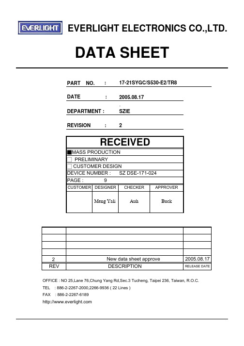
EVERLIGHT ELECTRONICS CO.,LTD.DATA SHEETPART NO. :17-21SYGC/S530-E2/TR8DATE :2005.08.17.DEPARTMENT:SZIEREVISION :2RECEIVED■MASS PRODUCTION□ PRELIMINARY□ CUSTOMER DESIGNDEVICE NUMBER : SZ DSE-171-024PAGE :9CUSTOMER DESIGNER CHECKER APPROVERMeng Yali Auh Buck2 New data sheet approve2005.08.17REV DESCRIPTION RELEASE DATEOFFICE : NO 25,Lane 76,Chung Yang Rd,Sec.3 Tucheng, Taipei 236, Taiwan, R.O.C.TEL : 886-2-2267-2000,2266-9936 ( 22 Lines )FAX : 886-2-2267-6189Technical Data Sheet0805 Package Chip LEDs17-21SYGC/S530-XX/TR8 Features․Package in 8mm tape on 7〞diameter reel.․Compatible with automatic placement equipment.․Compatible with infrared and vapor phase reflowsolder process.․Mono-color type.․Pb-free.․The product itself will remain within RoHS complaint Version.Descriptions․The 17-21 SMD Taping is much smallerthan lead frame type components, thusenable smaller board size, higher packingdensity, reduced storage space and finallysmaller equipment to be obtained.․Besides, lightweight makes them ideal forminiature applications. etc.Applications․Automotive: backlighting in dashboard and switch.․Telecommunication: indicator and backlighting intelephone and fax.․Flat backlight for LCD, switch and symbol.․General use.Device Selection GuideChipLens Color Part No.ColorMaterial Emitted17-21SYGC/S530-XX/TR8 AlGaInP Brilliant Yellow Green Water Clear17-21SYGC/S530-XX/TR8 Package Outline DimensionsNote: The tolerances unless mentioned is ±0.1mm, Unit = mm17-21SYGC/S530-XX/TR8Absolute Maximum Ratings (Ta=25℃)Parameter SymbolRating UnitReverse Voltage V R 5 V Forward Current I F 25 mA Operating Temperature Topr -40 ~ +85 ℃ Storage TemperatureTstg-40~ +90℃Electrostatic Discharge(HBM) ESD 2000 V Power Dissipation Pd 60mWPeak Forward Current (Duty 1/10 @1KHz) I FP60 mA Soldering TemperatureTsolReflow Soldering : 260 ℃ for 10 sec. Hand Soldering : 350 ℃ for 3 sec.Electro-Optical Characteristics (Ta=25℃)Parameter Symbol*ChipRankMin. Typ. Max. Unit ConditionE1 12 17 -----E2 17 23-----E3 22 31 ----- Luminous IntensityIvE4 27 41 -----mcdViewing Angle 2θ1/2 ----- ----- 140 ----- degPeak Wavelength λp ----- ----- 575 ----- nm Dominant Wavelength λd ----- ----- 573 ----- nm Spectrum RadiationBandwidth △λ ----- ----- 20 ----- nm Forward Voltage V F ----- 1.7 2.0 2.4 V I F =20 mAReverse CurrentI R----- ----- ----- 10μAV R =5V* Chip Rank17-21SYGC/S530-XX/TR8Reel DimensionsNote: The tolerances unless mentioned is ±0.1mm, Unit = mm17-21SYGC/S530-XX/TR8 Carrier Tape Dimensions: Loaded quantity3000 PCS per reel17-21SYGC/S530-XX/TR8Reliability Test Items And ConditionsThe reliability of products shall be satisfied with items listed below. Confidence level :90% LTPD :10%No. Items Test Condition Test Hours/Cycles SampleSizeAc/Re1 Reflow Soldering Temp. : 260℃±5℃Min. 5sec. 6 Min.22 PCS.0/1 2 Temperature Cycle H : +100℃ 15min∫ 5 minL : -40℃ 15min 300 Cycles 22 PCS.0/13 Thermal Shock H : +100℃ 5min∫ 10 secL : -10℃ 5min300 Cycles 22 PCS.0/1 4High TemperatureStorageTemp. : 100℃ 1000 Hrs. 22 PCS.0/1 5Low TemperatureStorage Temp. : -40℃ 1000 Hrs. 22 PCS.0/1 6 DC Operating Life I F = 20 mA 1000 Hrs. 22 PCS.0/1 7High Temperature /High Humidity85℃/ 85%RH1000 Hrs.22 PCS.0/117-21SYGC/S530-XX/TR8 Precautions For Use1. Over-current-proofCustomer must apply resistors for protection, otherwise slight voltage shift will cause bigcurrent change ( Burn out will happen ).2. Storage2.1 Do not open moisture proof bag before the products are ready to use.2.2 Before opening the package: The LEDs should be kept at 30℃or less and 90%RH or less.2.3 After opening the package : The LEDs should be kept at 30℃or less and 60%RH or less(Floor life).However, it's recommended that the LEDs should be used within 168 hours (7 days) after openingthe package. If unused LEDs remain, it should be stored in moisture proof packages.2.4 If the moisture absorbent material (silica gel) has faded away or the LEDs have exceeded thestorage time, baking treatment should be performed using the following conditions.Baking treatment : 60±5℃for 24 hours.3. Soldering Condition3.1 Pb-free solder temperature profile3.2 Reflow soldering should not be done more than two times.3.3 When soldering, do not put stress on the LEDs during heating.3.4 After soldering, do not warp the circuit board.17-21SYGC/S530-XX/TR84.Soldering IronEach terminal is to go to the tip of soldering iron temperature less than 350℃ for 3 seconds within once in less than the soldering iron capacity 25W. Leave two seconds and more intervals, and do soldering of each terminal. Be careful because the damage of the product is often started at the time of the hand solder. 5.RepairingRepair should not be done after the LEDs have been soldered. When repairing isunavoidable, a double-head soldering iron should be used (as below figure). It should be confirmed beforehand whether the characteristics of the LEDs will or will not be damaged by repairing.。
罗莫电子 Schottky 障碍管 RB521S-30说明书

Schottky Barrier DiodeRB521S-30●ApplicationsGeneral rectification●Features1)Ultra small mold type.(EMD2)2)Low V F3)High reliability●ConstructionSilicon epitaxial planar●Structure●Absolute maximum ratings (Ta=25°C)Symbol Unit V R V Io mA I FSM A Tj °C Tstg°C●Electrical characteristics (Ta=25°C)Symbol Min.Typ.Max.Unit Forward voltage V F--0.50V I F =200mA I R--30μAV R =10VParameter Limits Reverse voltage (DC)30Average rectified forward current 200Forward current surge peak (60Hz ・1cyc)1ConditionsJunction temperature 125Storage temperature-40 to +125Reverse currentParameterL a st0.010.1110100100010000100000102030FORWARD VOLTAGE:VF(mV)VF-IF CHARACTERISTICSF O R W A R D C U R R E N T :I F (m A )R E V E R S E C U R R E N T :I R (u A )REVERSE VOLTAGE:VR(V)VR-IR CHARACTERISTICSC A P A C I T A N C E B E T W E E N T E R M I N A L S :C t (p F )REVERSE VOLTAGE:VR(V)VR-Ct CHARACTERISTICSVF DISPERSION MAP F O R W A R D V O L T A G E :V F (m V )R E V E R S E C U R R E N T :V R (u A )IR DISPERSION MAPC A P A C I T A N C E B E T W E E N T E R M I N A L S :C t (p F )Ct DISPERSION MAPIFSM DISPERSION MAPP E A K S U R G E F O R W A R D C U R R E N T :I F S M (A )P E A K S U R G E F O R W A R D C U R R E N T :I F S M (A )NUMBER OF CYCLESIFSM-CYCLE CHARACTERISTICSP E A K S U R G E F O R W A R D C U R R E N T :I F S M (A )TIME:t(ms)IFSM-t CHARACTERISTICSTIME:(s)Rth-t CHARACTERISTICST R A N S I E N T T H A E R M A L I M P E D A N C E :R t h (℃/W )F O R W A R D P O W E R D I S S I P A T I O N :P f (W )AVERAGE RECTIFIED FORWARD CURRENT:Io(A)Io-Pf CHARACTERISTICSR E V E R S E P O W E R D I S S I P A T I O N P R (w )REVERSE VOLTAGE:VR(V)VR-P R CHARACTERISTICS10020030040050040041042043044045051015202530354045501011121314151617181920510152051011010005101101001010010000.0010.110100000.050.10.150.20.10.20.30.40.50.10.20.30.40.501020301101005101520L tAMBIENT TEMPERATURE:Ta(℃)Derating Curve゙A V E R A G E R E C T I F I D E F O R W A R D C U R R E N T I o (A )A V E R A G E R E C T I F I E D F O R W A R D C U R R E N T I o (A )CASE TEMPARATURE:Tc(℃)Derating Curve00.10.20.30.40.502550751001250.10.20.30.40.50255075100125L a st Ti me Bu yNoticePrecaution on using ROHM Products1. Our Products are designed and manufactured for application in ordinary electronic equipments (such as AV equipment,OA equipment, telecommunication equipment, home electronic appliances, amusement equipment, etc.). If youintend to use our Products in devices requiring extremely high reliability (such as medical equipment(Note 1), transport equipment, traffic equipment, aircraft/spacecraft, nuclear power controllers, fuel controllers, car equipment including car accessories, safety devices, etc.) and whose malfunction or failure may cause loss of human life, bodily injury or serious damage to property (“Specific Applications”), please consult with the ROHM sales representative in advance. Unless otherwise agreed in writing by ROHM in advance, ROHM shall not be in any way responsible or liable for any damages, expenses or losses incurred by you or third parties arising from the use of any ROHM’s Products for Specific Applications.(Note1) Medical Equipment Classification of the Specific ApplicationsJAPAN USA EU CHINA CLASS Ⅲ CLASS Ⅲ CLASS ⅡbCLASS ⅢCLASS Ⅳ CLASS Ⅲ2. ROHM designs and manufactures its Products subject to strict quality control system. However, semiconductorproducts can fail or malfunction at a certain rate. Please be sure to implement, at your own responsibilities, adequate safety measures including but not limited to fail-safe design against the physical injury, damage to any property, which a failure or malfunction of our Products may cause. The following are examples of safety measures:[a] Installation of protection circuits or other protective devices to improve system safety [b] Installation of redundant circuits to reduce the impact of single or multiple circuit failure3. Our Products are designed and manufactured for use under standard conditions and not under any special orextraordinary environments or conditions, as exemplified below. Accordingly, ROHM shall not be in any way responsible or liable for any damages, expenses or losses arising from the use of any ROHM’s Products under any special or extraordinary environments or conditions. If you intend to use our Products under any special or extraordinary environments or conditions (as exemplified below), your independent verification and confirmation of product performance, reliability, etc, prior to use, must be necessary:[a] Use of our Products in any types of liquid, including water, oils, chemicals, and organic solvents [b] Use of our Products outdoors or in places where the Products are exposed to direct sunlight or dust[c] Use of our Products in places where the Products are exposed to sea wind or corrosive gases, including Cl 2, H 2S, NH 3, SO 2, and NO 2[d] Use of our Products in places where the Products are exposed to static electricity or electromagnetic waves [e] Use of our Products in proximity to heat-producing components, plastic cords, or other flammable items [f] Sealing or coating our Products with resin or other coating materials[g] Use of our Products without cleaning residue of flux (even if you use no-clean type fluxes, cleaning residue of flux is recommended); or Washing our Products by using water or water-soluble cleaning agents for cleaning residue after soldering[h] Use of the Products in places subject to dew condensation4. The Products are not subject to radiation-proof design.5. Please verify and confirm characteristics of the final or mounted products in using the Products.6. In particular, if a transient load (a large amount of load applied in a short period of time, such as pulse. is applied,confirmation of performance characteristics after on-board mounting is strongly recommended. Avoid applying power exceeding normal rated power; exceeding the power rating under steady-state loading condition may negatively affect product performance and reliability.7. De-rate Power Dissipation (Pd) depending on Ambient temperature (Ta). When used in sealed area, confirm the actualambient temperature.8. Confirm that operation temperature is within the specified range described in the product specification.9. ROHM shall not be in any way responsible or liable for failure induced under deviant condition from what is defined inthis document.Precaution for Mounting / Circuit board design1. When a highly active halogenous (chlorine, bromine, etc.) flux is used, the residue of flux may negatively affect productperformance and reliability.2. In principle, the reflow soldering method must be used on a surface-mount products, the flow soldering method mustbe used on a through hole mount products. If the flow soldering method is preferred on a surface-mount products, please consult with the ROHM representative in advance. For details, please refer to ROHM Mounting specificationL a st Ti me Bu yPrecautions Regarding Application Examples and External Circuits1. If change is made to the constant of an external circuit, please allow a sufficient margin considering variations of thecharacteristics of the Products and external components, including transient characteristics, as well as static characteristics.2. You agree that application notes, reference designs, and associated data and information contained in this documentare presented only as guidance for Products use. Therefore, in case you use such information, you are solely responsible for it and you must exercise your own independent verification and judgment in the use of such information contained in this document. ROHM shall not be in any way responsible or liable for any damages, expenses or losses incurred by you or third parties arising from the use of such information.Precaution for ElectrostaticThis Product is electrostatic sensitive product, which may be damaged due to electrostatic discharge. Please take propercaution in your manufacturing process and storage so that voltage exceeding the Products maximum rating will not be applied to Products. Please take special care under dry condition (e.g. Grounding of human body / equipment / solder iron, isolation from charged objects, setting of Ionizer, friction prevention and temperature / humidity control).Precaution for Storage / Transportation1. Product performance and soldered connections may deteriorate if the Products are stored in the places where:[a] the Products are exposed to sea winds or corrosive gases, including Cl2, H2S, NH3, SO2, and NO2 [b] the temperature or humidity exceeds those recommended by ROHM [c] the Products are exposed to direct sunshine or condensation [d] the Products are exposed to high Electrostatic2. Even under ROHM recommended storage condition, solderability of products out of recommended storage time periodmay be degraded. It is strongly recommended to confirm solderability before using Products of which storage time is exceeding the recommended storage time period.3. Store / transport cartons in the correct direction, which is indicated on a carton with a symbol. Otherwise bent leadsmay occur due to excessive stress applied when dropping of a carton.4. Use Products within the specified time after opening a humidity barrier bag. Baking is required before using Products ofwhich storage time is exceeding the recommended storage time period.Precaution for Product Label QR code printed on ROHM Products label is for ROHM’s internal use only.Precaution for DispositionWhen disposing Products please dispose them properly using an authorized industry waste company.Precaution for Foreign Exchange and Foreign Trade actSince concerned goods might be fallen under listed items of export control prescribed by Foreign exchange and Foreign trade act, please consult with ROHM in case of export.Precaution Regarding Intellectual Property Rights1. All information and data including but not limited to application example contained in this document is for referenceonly. ROHM does not warrant that foregoing information or data will not infringe any intellectual property rights or any other rights of any third party regarding such information or data. 2. ROHM shall not have any obligations where the claims, actions or demands arising from the combination of theProducts with other articles such as components, circuits, systems or external equipment (including software).3. No license, expressly or implied, is granted hereby under any intellectual property rights or other rights of ROHM or anythird parties with respect to the Products or the information contained in this document. Provided, however, that ROHM will not assert its intellectual property rights or other rights against you or your customers to the extent necessary to manufacture or sell products containing the Products, subject to the terms and conditions herein. Other Precaution1. This document may not be reprinted or reproduced, in whole or in part, without prior written consent of ROHM.2. The Products may not be disassembled, converted, modified, reproduced or otherwise changed without prior writtenconsent of ROHM. 3. In no event shall you use in any way whatsoever the Products and the related technical information contained in theProducts or this document for any military purposes, including but not limited to, the development of mass-destruction weapons. 4. The proper names of companies or products described in this document are trademarks or registered trademarks ofROHM, its affiliated companies or third parties.L a st Ti me Bu yGeneral Precaution1. Before you use our Pro ducts, you are requested to care fully read this document and fully understand its contents.ROHM shall n ot be in an y way responsible or liabl e for fa ilure, malfunction or acci dent arising from the use of a ny ROHM’s Products against warning, caution or note contained in this document.2. All information contained in this docume nt is current as of the issuing date and subj ect to change without any priornotice. Before purchasing or using ROHM’s Products, please confirm the la test information with a ROHM sale s representative.3. The information contained in this doc ument is provi ded on an “as is” basis and ROHM does not warrant that allinformation contained in this document is accurate an d/or error-free. ROHM shall not be in an y way responsible or liable for any damages, expenses or losses incurred by you or third parties resulting from inaccuracy or errors of or concerning such information.L a st Ti me Bu y。
GE ADTS 530 气动测试设备说明书
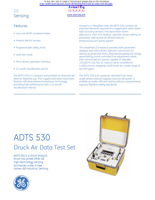
GESensingADTS 530ADTS 530 is a Druck product.Druck has joined other GE high–technology sensing businesses under a newname—GE Industrial, Sensing.gFeatures•Low cost RVSM compliant tester •Integral electric pumps •Programmable safety limits •Leak test mode•Menu driven operation interface •12 month recalibration periodThe ADTS 530 is a compact and portable air data test set ideal for flightline use. This rugged solid state instrument features vibrating element transducer technology,providing high performance with a 12 month recalibration interval.Druck Air Data Test SetHoused in a fiberglass case, the ADTS 530 contains all essential elements required of a rugged pitot static tester:high accuracy sensors, microprocessor drivenelectronics, clear LCD readout, operator driven valving for parameter setting and an efficient electric pressure/vacuum pump system.The simplified LCD readout provides both parameter displays and menu driven operator instructions forsetting up protective limits. Altitudes/airspeeds are simply generated by hand-controlled fine adjustment valves,with internal electric pumps capable of altitudes <55,000 ft (<16,764 m), rates of climb <6,000ft/min(<1828 m/min), airspeeds <650 knots, for a wide range of aircraft types.The ADTS 530 is AC powered, operated from most single-phase national supplies and aircraft power. Itenables accurate, efficient testing without compromising rigorous flightline safety standards./Druck-GE-Sensing-ADTS-530-Air-Data-Test-Set.aspxTo buy, sell, rent or trade-in this product please click on the link below:GeneralScaling Factors •Altitude: ft, meters •Airspeed: knots, km/Hr•Mach Rate of Climb: ft/min, m/min •Others: mbar, inHg, psigLeak Rate TestingDisplayed in ft/min/min and kts/min and km/hr/min Overpressure•Negligible calibration change with up to 2 x full scale (FS) overpressure applied.•Compliant with 97/23/EC (category SEP).Temperature Range•Calibrated: 32°F to 122°F (0°C to 50°C)•Operational: 32°F to 122°F (0°C to 50°C)•Storage: -4°F to 158°F (-20°C to 70°C)Conformity•EN61010 for electrical and mechanical safety •EMC Specification EN 61326-1. CE marked•89/336/EEC as amended by 92/31/EEC and 93/68/EEC Power Supply•115 V to 230 VAC •47 to 400 HzPhysical•Case Dimensions (w x h x d) 9.7 in x 15.4 in x 14.9 in (248 mm x 391 mm x 378 mm)•Weight 35 lb (16 kg) nominalCaseRugged fiberglass with removable lid and storage for accessories.Pneumatic Connections Ps and Pt _AN4 MaleADTS 530SpecificationsPneumatic SuppliesInternal pressure/vacuum pump to 55,000 ft/650 kts (16764 m/650 kts @ 6000 ft/min (1828.8 m/min)AccessoriesPitot static hoses 25 ft (8 m) long with AN4 mating fitting to one end. Universal probe adaptor for Ps and Pt, AC power cable. Operators manual and calibration certificate also supplied as standard.Calibration StandardsInstruments manufactured by GE are calibrated against precision equipment traceable to International Standards.Ordering InformationPlease state the following:1) Model type ADTS 530Parameter Operating Range Resolution Accuracy Repeatability Altitude -15,000 ft to 1 ft±3 ft (±0.91 m)±2 ft 55,000 ft (0.30 m)@ sea level (±0.60 m)(-4572 m to ±7 ft (±2.13 m)±2 ft 16764 m)@ 29,000 ft (±0.60 m)(8840 m)±9 ft ±19 ft (±5.79 m)(±2.74 m)@ 50,000 ft (15,240 m)Static 1.30 to 0.00014 psi ±0.0014 psi 0.00072 psi Sensor18.70 psia (0.01 mbar)(±0.1 mbar)(0.05 mbar)(90 to0.001 inHg ±0.003 inHg 0.0015 inHg 1290 mbar)(2.7 to 38 inHg)Airspeed 20 to 650 kts 0.1 kts ±1.0 kts @ 50±0.5 kts ±0.3 kts @ 200±0.15 kts ±0.1 kts @ 500±0.1 ktsPitot 1.30 psi to ±0.00014 psi ±0.0029 psi ±0.00072 psi Sensor37.70 psi (±0.01 mbar)(±0.2 mbar)rising to (90 mbar to 0.001 inHg±0.007 inHg0.0021 psi 2600 mbar)(±0.05 mbar (2.7 to 77 inHg)rising to 0.15 mbar)±0.015 inHg rising to ±0.005 inHg Timed 100 to1 ft/min ±1% of value±0.5% of valueRate of 20000 ft/min (0.30 m/min)Climb (30.48 to 6096 m/min)Mach 0.1 to 4.670.001*********±0.001falling to *********Engine 1 to 50.001RSS of Ps ±1 countPressure andPt sensor Ratio accuracy(E.P.R)g©2006 GE. All rights reserved.920-299BAll specifications are subject to change for product improvement without notice.GE ®is a registered trademark of General Electric Co. Other company or product names mentioned in this document may be trademarks or registered trademarks of their respective companies, which are not affiliated with GE.GESensing。
A264B-SYG-S530-E2-R中文资料

EVERLIGHT ELECTRONICS CO.,LTD.Technical Data Sheet5mm 1Pcs Circuit Board Indicator█ Features :●Low power consumption●High efficiency and low cost ●Good control and free combinations on the colors of LED lamps ●Good lock and easy to assembly ●Stackable and easy to assembly Stackable vertically and easy to assembly ●Versatile mounting on P.C board or panel ●Stackable horizontally and easy to assembly ●Pb free●The product itself will remain within RoHS compliant version█ Descriptions :●ARRAY=Plastic Holder+Combinations of Lamps●The array will easily mount the applicable lamps on any panel up to█ Applications :●ed as indicators of indicating the Degree, Functions, Positions etc, in electronic instruments.ChipMaterial Emitted Color264-10SYGD/S530-E2AlGaInPSuper Yellow GreenGreen DiffusedEVERLIGHT ELECTRONICS CO.,LTD.REV.:1Page: 1 of 6Device Number :CDAE-026-1252007/1/4Prepared by: Xiuzhen FengA264B/SYG/S530-E2/R/F14-47Lens Color PART NO. Prepared date:'http : //EVERLIGHT ELECTRONICS CO.,LTD.Technical Data Sheet5mm 1Pcs Circuit Board IndicatorPackage DimensionsNotes: 2.Lead spacing is measured where the lead emerge from the package█ Absolute Maximum Ratings at Ta = 25℃Parameter Symbol Rating Unit Forward CurrentIF 25mA Operating Temperature Topr -40 to +85℃Storage Temperature Tstg -40 to +100℃Soldering Temperature Tsol 260 ± 5℃Electrostatic Discharge ESD 2000V Power Dissipation Pd 60mW Reverse VoltageVR5VNote: *1:Soldering time ≦ 5 seconds.EVERLIGHT ELECTRONICS CO.,LTD http : // REV.:1Page: 2 0f 6Device Number :CDAE-026-125Prepared date:2007/1/4Prepared by:Xiuzhen Feng1.All dimensions are in millimeters, tolerance is 0.25mm except being specifiedA264B/SYG/S530-E2/R/F14-47EVERLIGHT ELECTRONICS CO.,LTD.Technical Data Sheet5mm 1Pcs Circuit Board IndicatorMin.Typ.Max.Unit I F =20mA / 2.0 2.4V V R =5V //10μA I F =20mA 2550/mcd I F =20mA /60/deg I F =20mA /575/nm I F =20mA /573/nm I F =20mA/20/nmEVERLIGHT ELECTRONICS CO.,LTD. http : // REV.:1Device Number :CDAE-026-125Prepared date:Prepared by:A264B/SYG/S530-E2/R/F14-47Electro-Optical Characteristics(Ta=25℃)2007/1/4λp λd △λV F I R Iv 2θ1/2Dominant Wavelength Spectrum RadiationBandwidthParameter Condition Forward Voltage Reverse Current Luminous Intensity Viewing Angle Peak Wavelength Symbol Xiuzhen FengPage:3 of 6EVERLIGHT ELECTRONICS CO.,LTD.EVERLIGHT ELECTRONICS CO.,LTD.Technical Data Sheet5mm 1Pcs Circuit Board Indicator█Reliability test items and conditions:The reliability of products shall be satisfied with items listed below. Confidence level:97% LTPD:3%NO Item Test ConditionsSample Size Failure Judgment Criteria1Solder Heat TEMP : 260℃ ± 5 ℃76 PCSH : +100℃ 15min2Temperature Cycle∫ 5 min 76 PCSL : -40℃ 15min H : +100℃ 5min3Thermal Shock ∫ 10 sec 76 PCSL : -10℃ 5min 4High Temperature Storage TEMP : 100℃76 PCS5Low Temperature Storage TEMP : -40℃76 PCSTEMP : 25℃I F = 20mA 7High Temperature / HighHumidity85℃ / 85% RH76 PCSNote:Ivt:To test Iv value of the chip before the reliablility testIv:The test value of the chip that has completed the reliablility test U:Upper Specification Limit L: Lower Specification LimitEVERLIGHT ELECTRONICS CO.,LTD. http : // REV.:1Device Number :CDAE-026-125Prepared date:Xiuzhen FengA264B/SYG/S530-E2/R/F14-47Test Hours/Cycle Ac/Re10 SECIv≦Ivt*0.5or Vf≧Uor Vf≦L 0/1300 CYCLES 1000 HRS76 PCS 6DC Operating Life 1000 HRS 0/1300 CYCLES 0/10/11000 HRS 0/10/1 Prepared by:2007/1/41000 HRS0/1Page:5 of 6EVERLIGHT ELECTRONICS CO.,LTD.Technical Data Sheet5mm 1Pcs Circuit Board Indicatormaximum ratings and the instructions included in these specification sheets.3. These specification sheets include materials protected under copyright of EVERLIGHT corporation. Please don't reproduce or cause anyone to reproduce them without EVERLIGHT'sconsent.EVERLIGHT ELECTRONICS CO.,LTD.http : // 'REV.:16 0f 6Device Number :CDAE-026-125Prepared date:2007/1/4Prepared by:Xiuzhen FengA264B/SYG/S530-E2/R/F14-47元器件交易网。
FA5305AP中文资料
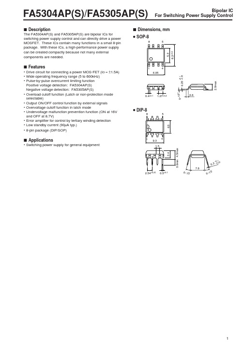
FA5304AP(S)/FA5305AP(S)1s DescriptionThe FA5304AP(S) and FA5305AP(S) are bipolar ICs forswitching power supply control and can directly drive a power MOSFET. These ICs contain many functions in a small 8-pin package. With these ICs, a high-performance power supply can be created compactly because not many external components are needed.s Features•Drive circuit for connecting a power MOS-FET (I O = ±1.5A)•Wide operating frequency range (5 to 600kHz)•Pulse-by-pulse overcurrent limiting function Positive voltage detection: FA5304AP(S)Negative voltage detection: FA5305AP(S)•Overload cutoff function (Latch or non-protection mode selectable)•Output ON/OFF control function by external signals •Overvoltage cutoff function in latch mode•Undervoltage malfunction prevention function (ON at 16V and OFF at 8.7V)•Error amplifier for control by tertiary winding detection •Low standby current (90µA typ.)•8-pin package (DIP/SOP)s Applications•Switching power supply for general equipments Dimensions, mm SOP-85DIP-8Bipolar ICFor Switching Power Supply ControlFA5304AP(S)/FA5305AP(S)0˚05元器件交易网FA5304AP(S)/FA5305AP(S)2s Block diagram FA5304AP(S)Pin Pin DescriptionNo.symbol1IN (–)Inverting input to error amplifier 2FB Error amplifier output 3IS (+)Overcurrent (+) detection 4GND Ground 5OUT Output 6VCC Power supply7CT Oscillator timing capacitor 8CSSoft-start and ON/OFF controlFA5305AP(S)PinPin DescriptionNo.symbol1IN (–)Inverting input to error amplifier 2FB Error amplifier output 3IS (–)Overcurrent (–) detection 4GND Ground 5OUT Output 6VCC Power supply7CT Oscillator timing capacitor 8CSSoft-start and ON/OFF controlFA5304AP(S)/FA5305AP(S)3s Absolute maximum ratingsCommon to FA5304AP(S) and FA5305AP(S)ItemSymbolRating Unit V CC 30V I O ±1.5A V IN 4V V FB 4V V IS –0.3 to +4V I CS 2mA P d 800 (DIP-8) *1mW 550 (SOP-8) *2T opr –30 to +85°C T stg–40 to +150°Cs Recommended operating conditions Common to FA5304AP(S) and FA5305AP(S)ItemSymbolMin.Max.Unit Supply voltageV CC1030V Error amplifier feedback resistor R NF 100k ΩSoft-start capacitor C S 0.11µF Oscillation frequency f OSC5600kHzSupply voltage Output current Error amplifier input voltageFeedback terminal input voltage Overcurrent detection terminal input voltage CS terminal input current Total power dissipation (Ta = 25°C)Operating temperature Storage temperatureNotes:*1Derating factor Ta > 25°C : 8.0mW/°C ( on PC board )*2Derating factor Ta > 25°C : 5.5mW/°C ( on PC board )s Electrical characteristics (Ta=25°C, V CC =18V,fosc=135kHz)Oscillator sectionCommon to FA5304AP(S) and FA5305AP(S)ItemSymbolTest conditionMin.Typ.Max.Unit Oscillation frequencyf OSCC T = 360pF112135148kHz Frequency variation 1 (due to supply voltage change)f dv V CC = 10 to 30V ±1%Frequency variation 2 (due to temperature change)f dTT a = –30 to +85°C±4%Error amplifier sectionCommon to FA5304AP(S) and FA5305AP(S))ItemSymbolTest conditionMin.Typ.Max.Unit Reference voltage V B 1.90 2.00 2.10V Input bias current I B V 1 = 2V–500–50nA Open-loop voltage gain A V 80dB Unity-gain bandwidthf T1.0MHz Maximum output voltage (Pin 2)V OM+R NF = 100k Ω2.70VV OM–R NF = 100k Ω200mVOutput source current (Pin 2)I MO+V OM = 1V–100–50µAPulse width modulation circuit sectionCommon to FA5304AP(S) and FA5305AP(S)ItemSymbolTest condition Min.Typ.Max.Unit Input threshold voltage (Pin 2)V TH FBO Duty cycle = 0%0.80 1.00 1.20V V TH FBM Duty cycle = D MAX1.70 1.902.10V Maximum duty cycleD MAX424550%Soft-start circuit sectionCommon to FA5304AP(S) and FA5305AP(S)ItemSymbolTest condition Min.Typ.Max.UnitCharge current (Pin 8)I CHGPin 8 = 0V –15–10–5µA Input threshold voltage (Pin 8)V TH CSO Duty cycle = 0%0.80 1.00 1.20V V TH CSMDuty cycle = D MAX1.701.902.10VFA5304AP(S)/FA5305AP(S)Overcurrent limiting circuit sectionItem Symbol Test condition FA5304AP(S)FA5305AP(S)UnitMin.Typ.Max.Min.Typ.Max. Input threshold voltage (Pin 3)V TH IS0.200.240.28–0.20–0.17–0.14V Overcurrent detection terminal source current I IS Pin 3 = 0V–300–200–100–240–160–80µA Delay time T PD IS150200nsLatch-mode cutoff circuit section Common to FA5304AP(S) and FA5305AP(S)Item Symbol Test condition Min.Typ.Max.Unit CS terminal sink current I SINK CS Pin 8 = 6V, Pin 2 = 1V4070150µA Cutoff threshold voltage (Pin 8)V TH CS 6.57.07.5VOverload cutoff circuit section Common to FA5304AP(S) and FA5305AP(S)Item Symbol Test condition Min.Typ.Max.Unit Cutoff threshold voltage (Pin 2)V TH FB 2.5 2.7 2.9VUndervoltage lock-out circuit section Common to FA5304AP(S) and FA5305AP(S)Item Symbol Test condition Min.Typ.Max.Unit OFF-to-ON threshold voltage V TH ON15.516.016.5V ON-to-OFF threshold voltage V TH OFF8.208.709.20V Voltage hysteresis V HYS7.30VOutput section Common to FA5304AP(S) and FA5305AP(S)Item Symbol Test condition Min.Typ.Max.Unit L-level output voltage V OL I O = 100mA 1.30 1.80VH-level output voltage V OH I O = –100mA, V CC = 18V16.016.5V Rise time tr No load50ns Fall time tf No load50nsOutput ON/OFF control circuit section Common to FA5304AP(S) and FA5305AP(S)Item Symbol Test condition Min.Typ.Max.Unit CS terminal source current I SOURCE CS Pin 8 = 0V–15–10–5µA OFF-to-ON threshold voltage (Pin 8)V TH ON CS pin voltage0.560.76V ON-to-OFF threshold voltage (Pin 8)V TH OFF CS pin voltage0.300.42VOverall device Common to FA5304AP(S) and FA5305AP(S)Item Symbol Test condition Min.Typ.Max.Unit Standby current I CC ST V CC = 14V90150µA Operating-state supply current I CC OP915mA OFF-state supply current I CC OFF 1.1 1.8mA Cutoff-state supply current I CCL 1.1 1.8mA45FA5304AP(S)/FA5305AP(S)Fig. 1 Configuration with error amplifierFig. 2 Configuration with optocoupler (FB pin input)Fig. 3 PWM comparatorFig. 4 PWM comparator timing charts Description of each circuit1. Oscillator (See block diagram on page 8.)The oscillator generates a triangular waveform by charging and discharging a capacitor. CT pin voltage oscillates between an upper limit of approx. 3.0V and a lower limit of approx. 1.0V. The oscillation frequency is determined by a external capacitance C T connected to CT pin, and approximately given by the following equation: (1)The recommended oscillation range is between 5k and 600kHz.The oscillator output is connected to a PWM comparator.2. Feedback circuitFigure 1 gives an example of connection in which built-in error amplifier is used to couple the feedback signal to IN(-) pin. Let n 2be the number of turns of secondary winding L 2 and n 3 be the number of turns of tertiary winding L 3. V CC and Vout are given by Vcc= 2(V)•(R 1+R 2)/R 2....................................(2)V OUT ȃ(n 2/n 3)•(Vcc+V D3)–V D2 (3)(where V D2 and V D3 are the forward voltage drops across diodes D 2and D 3 respectively).Here, the following equation must be satisfied to prevent from the malfunction of OUT pin at shutdown.(R1•R2)/ (R1+R2) 11k Ω (4)Figure 2 gives an example of connection in which anoptocoupler is used to couple the feedback signal to the FB pin. If this circuit causes power supply instability, the frequency gain can be decreased by connecting R 4 and C 4 as shown in figure 2. R 4 should be between several tens of ohms toseveral kiloohms and C 4 should be between several thousand picofarads to one microfarads.3. PWM comparatorThe PWM comparator has four inputs as shown in Figure 3.Oscillator output x is compared with CS pin voltage , FB pin , and DT voltage {. The lowest of three inputs , , and {is compared with output x . If it is lower than the oscillator output, the PWM comparator output is high, and if it is higher than the oscillator output, the PWM comparator output is low (see Fig. 4).The IC output voltage is high during when the comparator output is low, and the IC output voltage is low during when the comparator output is high.When the IC is powered up, CS pin voltage controls soft start operation. The output pulse then begins to widengradually. During normal operation, the output pulse width is determined within the maximum duty cycle (FA5304A,FA5305A: 45%) set by DT voltage { under the condition set by feedback signal , to stabilize the output voltage.C T (pF)f (kH Z ) =4.8 • 104FA5304AP(S)/FA5305AP(S)4. CS pin circuitAs shown in Figure 5, capacitor C S is connected to the CS pin. When power is turned on, the constant current source (10µA) begins to charge capacitor C S. Accordingly, the CS pin voltage rises as shown in Figure 6. The CS pin is connected to an input of the PWM comparator. The device is in soft-start mode while the CS pin voltage is between 1.0V and 1.9V common to FA5304A and FA5305A. During normal operation, the CS pin is clamped at 3.6V by internal zener diode Zn. If the output voltage drops due to an overload, etc., the clamp voltage shifts from 3.6V to 8.0V. As a result, the CS pin voltage rises to 8.0V. The CS pin is also connected to latch comparator C2. If the pin voltage rises above 7.0V, the output of comparator C2 goes high to turn off the bias circuit , thereby shutting the output down. Comparator C2 can be used not only for shutdown in response to an overload, but also for shutdown in response to an overvoltage. Comparator C1 is also connected to the CS pin, and the bias circuit is turned off and the output is shutdown if the CS pin voltage drops below 0.42V. In this way, comparator C1 can also be used for output on/off control.As explained above, the CS pin can be used for soft-start operation, overload and overvoltage output shutdown and output on/off control.Further details on the four functions of the CS pin are given below.4.1 Soft start functionFigure 7 shows the soft start circuit. Figure 8 is the soft-start operation timing chart. The CS pin is connected to capacitorC S . When power is turned on, a 10µA constant-current source begins to charge the capacitor. As shown in the timing chart, the CS pin voltage rises slowly in response to the charging current. The CS pin is connected internally to the PWM comparator. The comparator output pulse slowly widens as shown in the timing chart.The soft start period can be approximately evaluated by the period ts from the time the IC is activated to the time the output pulse width widens to 30%. Period ts is given by the following equation:t S (m S) = 160C S (µF) (2)Fig. 5 CS pin circuitFig. 6 CS pin waveformFig. 7 Soft-start circuit Fig. 8 Soft-start timing chart6FA5304AP(S)/FA5305AP(S) 4.2 Overload shutdownFigure 9 shows the overload shutdown circuit, and Figure 10 isa timing chart which illustrates overload shutdown operation.Ifthe output voltage drops due to an overload or short-circuit, theoutput voltage of the FB pin rises. If FB pin voltage exceedsthe reference voltage (2.7V) of comparator C3, the output ofcomparator C3 switches low to turn transistor Q off. In normaloperation, transistor Q is on and the CS pin is clamped at 3.6Vby zener diode Zn. With Q off, the clamp is released and the10µA constant-current source begins to charge capacitor C Sagain and the CS pin voltage rises. When the CS pin voltageexceeds the reference voltage (7.0V) of comparator C2, theoutput of comparator C2 switches high to turn the bias circuitoff. The IC then enters the latched mode and shuts the outputdown. Shutdown current consumption is 400µA(V CC=9V).This current must be supplied through the startup resistor. The IC then discharges the MOSFET gates.Shutdown operation initiated by an overload can be reset by lowering supply voltage V CC below 8.7V or forcing the CS pin voltage below 7.0V.The period t OL from the time that the output is short-circuited to the time that the bias circuit turns off is given by the following equation:t OL(m S) = 340Cs(µF) (3)4.3 Overvoltage shutdownFigure 11 shows the overvoltage shutdown circuit, and Figure 12 is a timing chart which illustrates overvoltage shutdown operation.The optocoupler PC1 is connected between the CS and V CC pins. If the output voltage rises too high, the PC1 turns on to raise the voltage at the CS pin via resistor R6. When the CS pin voltage exceeds the reference voltage (7.0V) of comparator C2, comparator C2 switches high to turn the bias circuit off. The IC then enters the latched mode and shuts the output down. The shutdown current consumption of the IC is 400µA(V CC=9V). This current must be applied via startup resistor R5.The IC then discharges the MOSFET gates.The shutdown operation initiated by an overvoltage condition can be reset by lowering supply voltage V CC below 8.7V or forcing the CS pin voltage below 7.0V.During normal operation, the CS pin is clamped by a 3.6V zener diode with a sink current of 150µA max. Therefore, a current of 150µA or more must be supplied by the optocoupler in order to raise the CS pin voltage above 7.0V.Fig. 9 Overload shutdown circuitFig. 10 Overload shutdown timing chartFig. 11 Overvoltage shutdown circuitFig. 12 Overvoltage shutdown timing chart78FA5304AP(S)/FA5305AP(S)4.4 Output ON/OFF controlThe IC can be turned on and off by an external signal applied to the CS pin.Figure 13 shows the external output on/off control circuit, and Figure 14 is the timing chart.The IC is turned off if the CS pin voltage falls below 0.42V. The output of comparator C1 switches high to turn the bias circuit off. This shuts the output down. The IC then discharges the MOSFET gates.The IC turns on if the CS pin is opened for automatic soft start.The power supply then restarts operation.5. Overcurrent limiting circuitThe overcurrent limiting circuit detects the peak value of every drain current pulse of the main switching MOSFET to limit the overcurrent.The detection threshold is +0.24V for FA5304A with respect to ground as shown in Figure 15.The drain current of the MOSFET is converted to voltage by resistor R 7 and fed to the IS pin of the IC. If the voltage exceeds the reference voltage (0.24V) of comparator C4, the output of comparator C4 goes high to set flip-flop output Q high. The output is immediately turned off to shut off the current. Flip-flop output Q is reset on the next cycle by the output of the PWM comparator to turn the output on again. This operation is repeated to limit the overcurrent.If the overcurrent limiting circuit malfunctions due to noise,place an RC filter between the IS pin and the MOSFET.Figure 16 is a timing chart which illustrates current-limiting operations.Fig. 13 External output on/off control circuitFig. 14 Timing chart for external output on/off controlFig. 16 Overcurrent timing chart for FA5304AFig. 15 Overcurrent limiting circuit for FA5304A9FA5304AP(S)/FA5305AP(S)The detection threshold is -0.17v for FA5305A with respect to ground as shown in Figure 17.The operation is similar to that of FA5304A except the threshold is minus voltage compared to that which is plus voltage for FA5304A.Figure 18 is a timing chart which illustrates current limiting operations.6. Undervoltage lockout circuitThe IC incorporates a circuit which prevents the IC from malfunctioning when the supply voltage drops. When the supply voltage is raised from 0V, the IC starts operation with V CC =16.0V.If the supply voltage drops, the IC shuts its output down when V CC =8.7V. When the undervoltage lockout circuit operates, the CS pin goes low to reset the IC.7. Output circuitAs shown in Figure 19, the IC’s totem-pole output can directly drive the MOSFET. The OUT pin can source and sink currents of up to 1.5A.If IC operation stops when the undervoltage lockout circuit operates, the gate voltage of the MOSFET goes low and the MOSFET is shut down.Fig. 17 Overcurrent limiting circuit for FA5305AFig. 18 Overcurrent timing chart for FA5305AFig. 19 Output circuitOUT pin outputH LComparator C4ReferenceOFFOvercurrent limitingMinus detectionFA5304AP(S)/FA5305AP(S)10s Design advice1. Startup circuitIt is necessary to start-up IC that the voltage inclination of VCC terminal “dVcc/dt” satisfies the following equation(4).dVcc/dt(V/s)>1.8/(Cs(µF)) (4)Cs : capacitor connected between CS terminal and GNDNote that equation (4) must be satisfied in any condition. Also,it is necessary to keep “latch mode” for overload protection or overvoltage protection that the current supplied to VCC terminal through startup resistor satisfies the following equation(5).Icc(Lat)>0.4mA for Vcc9.2V (5)Icc(Lat): Cutoff-state(=Latch mode) supply currentThe detail is explained as follows.(1) Startup circuit connected to AC line directlyFig. 20 shows a typical startup circuit that a startup resistor Rc is connected to AC line directly. The period from power-on to startup is determined by Rc, R D and C A . Rc, R D and C A must be designed to satisfy the following equations.dVcc/dt(V/s)=(1/C A ) • {(V AVE –Vccon )/R C –Vccon/R D –Iccst} >1.8/(Cs(µF)) (6)Rc(k Ω)< (V AVE –9.2(V))/{0.4 (mA) + (9.2(V)/R D (k Ω) } (7)V AVE = Vac • ǰ2/π: Average voltage applied to AC line side of Rc Vac:AC input effective voltageVccon:ON threshold of UVLO, 16.5V(max.)Iccst:Standby current, 0.15 mA(max.)In this method, Vcc voltage includes ripple voltage influenced by AC voltage. Therefore, enough dVcc/dt required byequation (6) tend to be achieved easily when Vcc reaches to Vccon even if Vcc goes up very slowly.After power-off, Vcc does not rise up because a voltageapplied from bias winding to VCC terminal decreases and the current flowing R C becomes zero, therefore, re-startup does not occur after Vcc falls down below OFF threshold of UVLO until next power-on.Fig. 20 Startup circuit example(1)FA5304AP(S)/FA5305AP(S)11(2) Startup circuit connected to rectified lineThis method is not suitable for FA5304A and FA5305A,especially concerned with re-startup operation just after power-off or startup which AC input voltage goes up slowly. Fig. 21shows a startup circuit that a startup resistor R A is connected to rectified line directly.The period from power-on to startup is determined by R A , R B and C A . R A , R B and C A must be designed to satisfy the following equations.dVcc/dt(V/s)=(1/C A )•{( V IN –Vccon )/R A – Vccon/R B –Iccst } >1.8/(Cs(µF)) (8)R A (k Ω)< (V IN – 9.2(V))/{0.4(mA) + (9.2(V)/R B (k Ω))}..............(9)V IN : ǰ2 •(AC input effective voltage)After power-off, once V CC falls down below OFF threshold voltage, V CC rises up again and re-startup occurs while the capacitor C 1 is discharged until approximately zero because V CC voltage rises up by the current flowing R A .This operation is repeated several times.After the repeated operation, IC stops in the condition that V CC voltage is equal to Vccon (=ON threshold) because capacitor C 1 is discharged gradually and the decreased V CC inclination is out of the condition required by equation (4).After that, re-startup by power-on can not be guaranteed even when equation (8) is satisfied. The image of that the startup is impossible is shown in Fig. 22. It is necessary to startup IC that supply current Icc (startup) to VCC is over 4mA in the condition of Tj < 100 °C during Vcc is kept at Vccon(Լ16V,balance state at Vccon after the repeated operation.Icc (start-up) > 4mA (10)at Vcc=Vccon, Tj<100°C, after power-offThis balance state that startup is impossible tends to occur at higher temperature.If power-on is done when Vcc is not kept at Vccon (forexample: power-off is done and after enough time that C 1 is discharged until Vcc can not be pulled up to Vccon), the IC can startup in the condition given by equation(8).In some cases, such as when the load current of power supply is changed rapidly, you may want to prolong the hold time of the power supply output by means of maintaining Vcc over the off threshold.For this purpose, connect diode D 4 and electrolytic capacitor C 4 as shown in Fig. 23. This prolongs the hold time of thepower supply voltage Vcc regardless of the period from power-on to startup.Fig. 21 Startup circuit example(2)Fig. 23 Startup circuit example(3)Startup is impossible (dVcc/dt <1.8/Cs just before Vcc reaches Vccon).Icc>4mA is necessary for startup atFig. 22 Image of Vcc waveform when re-startup is impossibleFA5304AP(S)/FA5305AP(S)122. Disabling overload shutdown functionAs shown in Figure 24, connect a 330k Ω to 470k Ω resistor between the CS pin and ground. Then, the CS pin voltage does not rise high enough to reach the reference voltage (7.0V) of the latch comparator, and the IC does not enter the OFF latch mode. With this connection, the overvoltage shutdown function is not available.3. Setting soft start period and OFF latch delay independentlyFigure 25 shows a circuit for setting the soft start period and OFF latch delay independently. In this circuit, capacitance C S determines the soft start period, and capacitance C Ldetermines the OFF latch delay. If the overload shutdown and overvoltage shutdown functions raise the CS pin voltage to around 5V, zener diode Zn becomes conductive to charge C L .The OFF latch delay can be thus prolonged by C L .4. Laying out Vcc and ground linesFigure 26 and Figure 27 show the recommended layouts of V CC and ground lines. The bold lines represent paths carrying large currents. The lines must have an adequate thickness.5. Sink current setting for CS terminalA sink current to CS terminal must be satisfied the following condition to prevent from the malfunction which uncontrolled pulse output generates at OUT terminal when latch-mode protection should be operated for overvoltage.150µA < Ics(sink) < 500µA at Vcs= 6.5(V)Ics(sink): Sink current to CS terminalExample (for the circuit shown in Fig. 28 )Ics(sink) = (28(V)–18(V)– 6.5(V))/7.5(k Ω) Լ 467 (µA) < 500 (µA)Fig. 25 Independent setting of soft-start period and OFF latchdelayFig. 26 Vcc line and ground line for FA5304AFig. 24 Disabling overload shutdown functionFig. 27 Vcc line and ground line for FA5305AFig. 28 Setting sink current for CS terminalFA5304AP(S)/FA5305AP(S)13s Characteristic curves (Ta = 25°C)Oscillation frequency (f OSC ) vs.Oscillation frequency (f OSC ) vs.timing capacitor capacitance (C T )ambient temperature (Ta)Output duty cycle vs. FB terminal voltage (V FB )Output duty cycle vs. FB terminal source current (Isource)Output duty cycle vs. CS terminal voltage (V CS )H-level output voltage (V OH ) vs.output source current (I SOURCE)FA5304AP(S)/FA5305AP(S)14L-level output voltage (V OL ) vs.IS (+) terminal threshold voltage (V TH IS(+)) vs.output sink current (I SINK )ambient temperature (Ta)FA5304AP(S)IS (–) terminal threshold voltage (V TH IS(–)) vs.IS (+) terminal current (I IS(+)) vs.ambient temperature (Ta)IS (+) terminal voltage (V IS(+))FA5305AP(S)FA5304AP(S)IS (–) terminal current (I IS(–)) vs.CS terminal sink current (I SINK CS ) vs.IS (–) terminal voltage (V IS(–))CS terminal voltage (V CS )FA5305AP(S)V O L [V ]I SINK [A]FA5304AP(S)/FA5305AP(S)15Error amplifier frequency (f) vs. voltage gain (Av) /phase (θ)Supply current (I CC ) vs. supply voltage (V CC )Normal operationSupply current (I CC ) vs. supply voltage (V CC )OFF or OFF latch modeFA5304AP(S)/FA5305AP(S)16s Application circuitExample of FA5304AP(S) application circuit (1)Example of FA5304AP(S) application circuit (2)FA5304AP(S)/FA5305AP(S)17Example of FA5304AP(S) application circuit (3)Example of FA5305AP(S) application circuitParts tolerances characteristics are not defined in the circuit design sample shown above. When designing an actual circuit for a product,you must determine parts tolerances and characteristics for safe and economical operation.。
Eutectic EuTronic Arc 525AS产品说明书

爱立光 LAMP 333-2UYD S530-A3-L 产品说明书
LAMP333-2UYD/S530-A3-LFeatures• Choice of various viewing angles • Available on tape and reel. • Reliable and robust • Pb free • The product itself will remain within RoHS compliant version. Description •The series is specially designed for applications requiring higher brightness •The led lamps are available with different colors, intensities.. Applications • TV set • Monitor • Telephone • ComputerDevice Selection GuideChipEmitted Color Resin Color MaterialsAlGaInP Brilliant Yellow Yellow Diffused Absolute Maximum Ratings (Ta=25℃)Parameter Symbol Rating Unit Continuous Forward Current I F25 mAPeak Forward Current (Duty 1/10 @ 1KHZ) I FP60 mAElectrostatic Discharge ESD(HBM) 2000 VReverse Voltage V R 5 VPower Dissipation P d 60 mWOperating Temperature T opr-40 ~ +85 ℃Storage Temperature Tstg -40 ~ +100 ℃Soldering Temperature T260 ℃for 5 sec.solElectro-Optical Characteristics (Ta=25℃)Parameter Symbol Min. Typ. Max. Unit Condition Luminous Intensity Iv 160 320 ----- mcd I F=20mA Viewing Angle 2θ1/2----- 35 ----- deg I F=20mA Peak Wavelength λp----- 591 ----- nm I F=20mA Dominant Wavelength λd----- 589 ----- nm I F=20mA Spectrum Radiation Bandwidth Δλ----- 15 ----- nm I F=20mA Forward Voltage V F 2.0 2.4 V I F=20mA Reverse Current I R----- ----- 10 μA V R=5V *Measurement Uncertainty of Luminous Intensity: ±10%*Measurement Uncertainty of Dominant Wavelength ±1.0nm*Measurement Uncertainty of Forward Voltage: ±0.1VTypical Electro-Optical Characteristics CurvesRelative Intensity vs. Wavelength (Ta=25℃) Directivity (Ta=25℃)R e l a t i v e I n t e n s i t y (a .u .)R a d i a t i o n A n g l eWavelength (nm)Relative Intensity (a.u.)Forward Current vs. Forward Voltage (Ta=25℃)Relative Intensity vs. Forward Current (Ta=25℃)F o r w a r d C u r r e n t (m A )1.52.0 2.53.0 3.54.04.5051015202530F o r w a r d C u r r e n t (m A )Forward Voltage(V)R e l a t i v e I n t e n s i t y (a .u .)Forward Voltage (V)Forward Current (mA)Relative Intensity vs. Ambient Temp.Forward Current vs. Ambient Temp.R e l a t i v e I n t e n s i t y (a .u .)F o r w a r d C u r r e n t (m A )Ambient Temperature Ta (℃)Ambient Temperature Ta (℃)Package DimensionNote: Note:1. All dimensions are in millimeters2. The height of flange must be less than 1.5mm(0.059").3. Without special declared, the tolerance is ±0.25mm.PbMoisture Resistant Packing MaterialsLabel ExplanationCPN: Customer's Production Number P/N : Production Number QTY: Packing Quantity CAT: RanksHUE: Dominant Wavelength REF: Reference LOT No: Lot NumberPacking Specification■ Anti -electrostatic bag ■ Inner Carton ■ Outside Carton■ Packing Quantity1.Min200~500 PCS/1 Bag, 5 Bags/1 Inner Carton2. 10 Inner Cartons/1 Outside CartonPreheadlaminar waveFluxingNotes1. Lead Forming⏹ During lead formation, the leads should be bent at a point at least 3mm from the base of the epoxy bulb.⏹ Lead forming should be done before soldering.⏹ Avoid stressing the LED package during leads forming. The stress to the base may damage the LED’s characteristics or it may break the LEDs.⏹ Cut the LED lead frames at room temperature. Cutting the lead frames at high temperatures may cause failure of the LEDs. ⏹When mounting the LEDs onto a PCB, the PCB holes must be aligned exactly with the lead position of the LED. If the LEDs are mounted with stress at the leads, it causes deterioration of the epoxy resin and this will degrade the LEDs.2. Storage ⏹ The LEDs should be stored at 30°C or less and 70%RH or less after being shipped from Everlight and the storage life limitsare 3 months. If the LEDs are stored for 3 months or more, they can be stored for a year in a sealed container with a nitrogen atmosphere and moisture absorbent material. ⏹Please avoid rapid transitions in ambient temperature, especially, in high humidity environments where condensation can occur.3. Soldering ⏹ Careful attention should be paid during soldering. When soldering, leave more then 3mm from solder joint to epoxy bulb,and soldering beyond the base of the tie bar is recommended. ⏹Recommended soldering conditions:Hand SolderingDIP SolderingTemp. at tip of iron300℃ Max. (30W Max.) Preheat temp.100℃ Max. (60 sec Max.) Soldering time 3 sec Max. Bath temp. & time 260 Max., 5 sec Max Distance 3mm Min.(From solderjoint to epoxy bulb)Distance 3mm Min. (From solderjoint to epoxy bulb)⏹ Recommended soldering profile⏹ Avoiding applying any stress to the lead frame while the LEDs are at high temperature particularly when soldering. ⏹ Dip and hand soldering should not be done more than one time⏹ After soldering the LEDs, the epoxy bulb should be protected from mechanical shock or vibration until the LEDs return to room temperature.⏹A rapid-rate process is not recommended for cooling the LEDs down from the peak temperature.⏹Although the recommended soldering conditions are specified in the above table, dip or hand soldering at the lowestpossible temperature is desirable for the LEDs.⏹Wave soldering parameter must be set and maintain according to recommended temperature and dwell time in the solderwave.4. Cleaning⏹When necessary, cleaning should occur only with isopropyl alcohol at room temperature for a duration of no more thanone minute. Dry at room temperature before use.⏹Do not clean the LEDs by the ultrasonic. When it is absolutely necessary, the influence of ultrasonic cleaning on the LEDsdepends on factors such as ultrasonic power and the assembled condition. Ultrasonic cleaning shall be pre-qualified to ensure this will not cause damage to the LED5. Heat Management⏹Heat management of LEDs must be taken into consideration during the design stage of LED application. The currentshould be de-rated appropriately by referring to the de-rating curve found in each product specification.⏹The temperature surrounding the LED in the application should be controlled. Please refer to the data sheet de-ratingcurve.6. ESD (Electrostatic Discharge)⏹The products are sensitive to static electricity or surge voltage. ESD can damage a die and its reliability.When handling the products, the following measures against electrostatic discharge are stronglyrecommended:Eliminating the chargeGrounded wrist strap, ESD footwear, clothes, and floorsGrounded workstation equipment and toolsESD table/shelf mat made of conductive materials⏹Proper grounding is required for all devices, equipment, and machinery used in product assembly.Surge protection should be considered when designing of commercial products.⏹If tools or equipment contain insulating materials such as glass or plastic,the following measures against electrostatic discharge are strongly recommended:Dissipating static charge with conductive materialsPreventing charge generation with moistureNeutralizing the charge with ionizers7. Other⏹Above specification may be changed without notice. EVERLIGHT will reserve authority on material change for abovespecification.⏹When using this product, please observe the absolute maximum ratings and the instructions for using outlined in thesespecification sheets. EVERLIGHT assumes no responsibility for any damage resulting from use of the product which does not complywith the absolute maximum ratings and the instructions included in these specification sheets.⏹These specification sheets include materials protected under copyright of EVERLIGHT corporation. Please don’treproduce or cause anyone to reproduce them without EVERLIGHT’s consent.DISCLAIMER1. EVERLIGHT reserves the right(s) on the adjustment of product material mix for the specification.2. The product meets EVERLIGHT published specification for a period of twelve (12) months from date of shipment.3. The graphs shown in this datasheet are representing typical data only and do not show guaranteed values.4. When using this product, please observe the absolute maximum ratings and the instructions for using outlined in thesespecification sheets. EVERLIGHT assumes no responsibility for any damage resulting from the use of the product which does not comply with the absolute maximum ratings and the instructions included in these specification sheets.5. These specification sheets include materials protected under copyright of EVERLIGHT. Reproduction in any form isprohibited without obtaining EVERLIGHT’s prior consent.6. This product is not intended to be used for military, aircraft, automotive, medical, life sustaining or life saving applications orany other application which can result in human injury or death. Please contact authorized Everlight sales agent for special application request.。
APS Series LWU650-APS, LWU530-APS 使用者手冊 (完整版) 網路指南
特點
本投影機具有網路功能,可為您帶來以下主要功能。
ü WEB 控制 : 可讓您透過網路從電腦、智慧型手機和平板設備監控投影機。(&35) ü 網絡演示 : 可讓投影機投影透過網路傳輸的電腦影像。(&77) ü 我的圖像 : 可讓投影機最多儲存四個靜止影像並進行投影。(&81) ü 信差 : 可讓投影機透過網路顯示從電腦傳送的文本。(&82) ü 網路橋接器 : 可讓您從電腦透過投影機控制外部設備。(&85)
3.1.3.1 一般設定 .............................................................. 41 3.1.3.2 無線設定 .............................................................. 43 3.1.3.3 有線設定 .............................................................. 46 3.1.3.4 其他設定 .............................................................. 47 3.1.4 連接埠設定 ............................................................... 48 3.1.5 郵件設定 ................................................................. 50 3.1.6 警報設定 ................................................................. 52 3.1.7 排程設定 ................................................................. 53 3.1.7.1 排程管理 .............................................................. 53 3.1.7.2 編程列表 .............................................................. 54 3.1.7.3 編程編輯 .............................................................. 55 3.1.7.4 編程副本 .............................................................. 56
Alpha Wire 产品说明书:3530型号
Alpha Wire | 711 Lidgerwood Avenue, Elizabeth, NJ 07207Tel: 1-800-52 ALPHA (25742), Web: Customer SpecificationPART NO. 3530ConstructionDiameters (In)1) Component 1 10 X 1 CONDa) Conductor 22 (19/34) AWG TC 0.032b) Insulation 0.010" Wall, Nom. PVC 0.052(1) Color(s)Cond Color Cond Color Cond Color1 BROWN 5 GREEN9 WHITE2 RED 6 BLUE10 BLACK3 ORANGE 7 VILOET4 YELLOW 8 SLATE2) Cable Assembly 10 Components assembled parallel.0.052 +/- 0.002 x0.520 +/- 0.020Applicable Specifications1) UL AWM/STYLE 2713 80°C / 150 V RMSVW-12) Militarya) Component 1MIL-DTL-16878/1 (Type B) 105°C / 600 V RMS Environmental1) EU Directive 2011/65/EU(RoHS2):All materials used in the manufacture of this part are in compliance with European Directive2011/65/EU regarding the restriction of use of certain hazardous substances in electrical andelectronic equipment. Consult Alpha Wire's web site for RoHS C of C.2) REACH Regulation (EC 1907/2006):This product does not contain Substances of Very High Concern (SVHC) listed on the EuropeanUnion's REACH candidate list in excess of 0.1% mass of the item. For up-to-date information,please see Alpha's REACH SVHC Declaration.3) California Proposition 65:The outer surface materials used in the manufacture of this part meet the requirements of California Proposition 65.PropertiesPhysical & Mechanical Properties1) Temperature Range-55 to 105°C2) Bend Radius 10X Cable Diameter3) Pull Tension 59 Lbs, MaximumElectrical Properties(For Engineering purposes only)1) Voltage Rating 600 V RMS2) Capacitance 34 pf/ft @1 kHz, Nominal Conductor to Conductor3) Inductance0.17 µH/ft, Nominal4) Conductor DCR15.1 Ω/1000ft @20°C, NominalOtherPackaging Flange x Traverse x Barrel (inches)a) 100 FT11 x 0.75 x 3 Continuous length[Spool dimensions may vary slightly]Alpha Wire | 711 Lidgerwood Avenue, Elizabeth, NJ 07207Tel: 1-800-52 ALPHA (25742)Although Alpha Wire (“Alpha”) makes every reasonable effort to ensure their accuracy at the time of publication, information and specifications described herein are subject to errors or omissions and to changes without notice, and the listing of such information and specifications does not ensure product availability.Alpha provides the information and specifications herein on an “AS IS” basis, with no representations or warranties, whether express, statutory or implied. In no event will Alpha be liable for any damages (including consequential, indirect, incidental, special, punitive, or exemplary) whatsoever, even if Alpha had been advised of the possibility of such damages, whether in an action under contract, negligence or any other theory, arising out of or in connection with the use, or inability to use, the information or specifications described herein.ALPHA WIRE - CONFIDENTIAL AND PROPRIETARYNotice to persons receiving this document and/or technical information. This document is confidential and is the exclusive property of ALPHA WIRE, and is merely on loan and subject to recall by ALPHA WIRE at any time. By taking possession of this document, the recipient acknowledges and agrees that this document cannot be used in any manner adverse to the interests of ALPHA WIRE, and that no portion of this document may be copied or otherwise reproduced without the prior written consent of ALPHA WIRE. In the case of conflicting contractual provisions, this notice shall govern the status of this document. ©2013 ALPHA WIRE - all rights reserved.EU/China ROHS CERTIFICATE OF COMPLIANCETo Whom It May Concern:Alpha Wire Part Number: 35303530 , RoHS-Compliant Commencing With 3/1/2005 ProductionNote: all colors and put-upsThis document certifies that the Alpha part number cited above is manufactured in accordance with Directive 2011/65/EU of the European Parliament, better known as the RoHS Directive (commonly known as RoHS 2), with regards to restrictions of the use of certain hazardous substances used in the manufacture of electrical and electronic equipment. This certification extends to amending Directive 2015/863/EU which expanded the list of restricted substances to 10 items (commonly known as RoHS 3) The reader is referred to these Directives for the specific definitions and extents of the Directives. No Exemptions are required for RoHS Compliance on this item. Additionally, Alpha certifies that the listed part number is in compliance with China RoHS “Marking for Control of Pollution by Electronic Information Products” standard SJ/T 11364-2014. Substance Maximum Control ValueLead0.1% by weight (1000 ppm)Mercury0.1% by weight (1000 ppm)Cadmium0.01% by weight (100 ppm)Hexavalent Chromium0.1% by weight (1000 ppm )Polybrominated Biphenyls (PBB)0.1% by weight (1000 ppm)Polybrominated Diphenyl Ethers (PBDE) ,Including Deca-BDE0.1% by weight (1000 ppm)Bis(2-ethylhexyl) phthalate (DEHP)0.1% by weight (1000 ppm)Butyl benzyl phthalate (BBP)0.1% by weight (1000 ppm)Dibutyl phthalate (DBP) 0.1% by weight (1000 ppm)Diisobutyl phthalate (DIBP)0.1% by weight (1000 ppm)The information provided in this document and disclosure is correct to the best of Alpha Wire's knowledge, information and belief at the date of its release. The information provided is designed only as a general guide for the safe handling, storage, and any other operation of the product itself or the one that it will become part of. The intent of this document is not to be considered a warranty or quality specification. Regulatory information is for guidance purposes only. Product users are responsible for determining the applicability of legislation and regulations based on their individual usage of the product.Authorized Signatory for the Alpha Wire:Dave Watson, Director of Engineering & QA12/28/2017Alpha Wire711 Lidgerwood Ave.Elizabeth, NJ 07207Tel: 1-908-925-8000。
海帆5300(5300-2)规格说明书
access via deck hatch.
ENGINE • Engine throttle in the cockpit with removable
handle, • Engine panel, • Sound insulation for engine compartment, • Access via removable companionway, • Diesel engine Yanmar 3YM20C - 21 HP,
control lines, • 2 winches Harken Performa for genoa and
spinnaker,
• 2 winches Harken Quattro on coachroof for halyards and control lines,
• 2 turning blocks for genoa sheets, • 2 tracks for genoa lead cars on sidedecks, • Chainplates for shrouds on side of hull, • Chainplates for backstay, • Deck Step for mast with blocks, • Handrails on coachroof.
positions.
STEERING • Double polyester rudders and stainless steel
rudder stocks, • Self-aligning rudder bearings.
RIGGING • Deck-stepped mast, • 2 levels of pushing spreaders - 19/20 fractional, • Stainless steel Dyform® shrouds, • Adjustable backstay with returns to each helm, • Forestay with hardware for hanked-on sail,
- 1、下载文档前请自行甄别文档内容的完整性,平台不提供额外的编辑、内容补充、找答案等附加服务。
- 2、"仅部分预览"的文档,不可在线预览部分如存在完整性等问题,可反馈申请退款(可完整预览的文档不适用该条件!)。
- 3、如文档侵犯您的权益,请联系客服反馈,我们会尽快为您处理(人工客服工作时间:9:00-18:30)。
EVERLIGHT ELECTRONICS CO.,LTD.Technical Data Sheet0.54" Dual Digit Alphanumeric DisplaysELD-525SYGWA/S530-E2█ Features :●Industrial standard size. ●Low power consumption.●Categorized for luminous intensity.●Pb free●The product itself will remain within RoHS compliant version█ Descriptions :●The ELD-525 series is a large 13.6 mm (0.54")high seven segment display designed for viewing distances up to 7 meters.●These displays provide excellent reliability in bright ambient light. ●These devices are made with white segments and gray surface.█ Applications :●Audio equipment ●Instrument panels ●Digital read out displayMaterialAlGaInPBG0511038 50011389EVERLIGHT ELECTRONICS CO.,LTD.http : // Rev. : 1Page: 1 of 6Prepared date:2006/4/3Prepared by: YanLi ZhongDevice Number : CDDD-525-010ELD-525SYGWA/S530-E2PART NO.Emitted Color Super Yellow GreenChipEVERLIGHT ELECTRONICS CO.,LTD. Technical Data SheetEVERLIGHT ELECTRONICS CO.,LTD.Technical Data Sheet0.54" Dual Digit Alphanumeric DisplaysELD-525SYGWA/S530-E2█Absolute maximum ratings at Ta = 25℃:Parameter Symbol Rating Unit Reverse Voltage V R 5V Forward Current I F 25mA Operating Temperature Topr -40 to +85℃Storage Temperature Tstg -40 to +100℃Soldering Temperature *Tsol 260 ± 5℃Electrostatic Discharge ESD 2000V Power DissipationPd60mWNote: *Soldering time ≦ 5 seconds.█Electronic optical characteristics :ParameterSymbolMin.Typ.Max.Unit Condition ---- 1.5----mcdI F =2mALuminous 2.84.5----mcdI F =10mA----0.6----mcdI F =2mA1.02.0----mcd I F =10mA Peak Wavelength λp ----575----nm I F =20mA Dominant Wavelength λd ----573----nm I F =20mA △λ----20----nm I F =20mA Forward Voltage V F ----- 2.0 2.4V I F =20mA Reverse CurrentI R--------100μAV R =5VEVERLIGHT ELECTRONICS CO.,LTD. http : // Rev. : 1Page: 3 of 6Device Number : CDDD-525-010Prepared date:2006/4/3Prepared by: YanLi ZhongIvSpectrum RadiationBandwidth IntensityPer segmentPer decimal pointEVERLIGHT ELECTRONICS CO.,LTD.Technical Data Sheet0.54" Dual Digit Alphanumeric DisplaysELD-525SYGWA/S530-E2█ Typical Electro-Optical Characteristic Curves:EVERLIGHT ELECTRONICS CO.,LTD.http : // Rev. : 1Page: 4 of 6 Device Number : CDDD-525-010Prepared date:2006/4/3Prepared by: YanLi ZhongTechnical Data Sheet0.54" Dual Digit Alphanumeric DisplaysELD-525SYGWA/S530-E2█ Reliability test items and conditions:The reliability of products shall be satisfied with items listed below. Confidence level:97% LTPD:3%NOItemTest ConditionsTest Hours/Cycle Sample SizeFailure Judgment CriteriaAc/Re1Solder Heat TEMP : 260℃ ± 5 ℃ 5 SEC76 PCS 0/1H : +85℃ 30min 2Temperature Cycle ∫ 5 min 50 CYCLE 76 PCS 0/1L : -55℃ 30min H : +100℃ 5min 3Thermal Shock ∫ 10 sec 50 CYCLE 76 PCS0/1L : -10℃ 5min 4High Temperature Storage TEMP : 100℃1000 HRS 76 PCS0/15Low Temperature Storage TEMP : -55℃1000 HRS 76 PCS 0/16DC Operating Life IF = 10 mA 1000 HRS 76 PCS 0/17High Temperature / HighHumidity85℃/85% RH 1000 HRS 76 PCS 0/1Note:Ivt:The test Iv value of the chip before the reliablility testIv:The test value of the chip that has completed the reliablility test U:Upper Specification Limit L: Lower Specification Limithttp : // Rev. : 1Page: 5 of 6Device Number : CDDD-525-010Prepared date:2006/4/3Prepared by: YanLi ZhongIv≦Ivt*0.5or Vf≧U or Vf≦LEVERLIGHT ELECTRONICS CO.,LTD.Technical Data Sheet0.54" Dual Digit Alphanumeric DisplaysELD-525SYGWA/S530-E2█ Packing Quantity Specification1. 20PCS/tube, 36 tubes/box1. Above specification may be changed without notice. EVERLIGHT will reserve authority onmaterial change for above specification.2. When using this product, please observe the absolute maximum ratings and the instructionsfor using outlined in these specification sheets. EVERLIGHT assumes no responsibility forany damage resulting from use of the product which does not comply with the absolutemaximum ratings and the instructions included in these specification sheets.3. These specification sheets include materials protected under copyright of EVERLIGHT corporation.Please don't reproduce or cause anyone to reproduce them without EVERLIGHT'sconsent.EVERLIGHT ELECTRONICS CO.,LTD.http : // Rev. : 1 Page: 6 of 6 Device Number : CDDD-525-010Prepared date:2006/4/3Prepared by: YanLi Zhong。