ARM_Cortex介绍
ARM Cortex

ARM Cortex—M3处理器ARM Cortex—M3处理器为性能高。
低成本的平台提供一个满足小存储器要求的方案。
简化管脚数。
以及低功耗三方面要求的内核,与此同时,它还提供出色的计算机性能和优越的系统响应能力;特性:紧凑的内核1.Thumb-2的指令集。
在通常与8位和16位设备相关的存储器量中,特别是在微控制器几应用中的几千字节存储量中,提供ARM内核所期望的高性能;2.高速的应用通过Harvard结构执行,以独立的指令和数据中线为特证,3.优越的中断处理能力,通过执行寄存器操作来实现的,这些寄存器操作在处理硬件中断是使用4.存储器保护单元(MPU)为复杂的应用提高特权的操作模式,5.从ARM7处理器系列中移植出来,已获得更好的性能和电源效率。
6.功能齐全的解决方案:—串行线JTAG调试端口(AWJ-DP)__Flash 修补和端口(FBP)单元,用于实现断电操作—数据观察点和触发(DWT)单元,用于执行观察点、触发源和系统性能分析(数据跟踪源)—仪表跟踪宏单元(ITM),用于支持printf 型调试(调试消息)—跟踪端口接口单元(TPIU)用作跟踪端口分析仪的桥接1.2 处理器的组件这节内容描述了Cortex-M3 处理器的组件,系统的主要模块包括:1 处理器内核2 NVIC3 总线矩阵4FPB5 DWT6 ITM7 MPU8 ETM9 TPIU1.串行线JTAG调试端口:测试访问端口和边界扫描结构标准.主要应用于:电路的边界扫描测试和可编程芯片的在线系统编程。
2.闪存地址重载及断点单元(FPB)硬件断点支持。
产生一个断点事件,从而使处理器进入调试模式3.数据观察点与跟踪(DWT)它包含比较器,可以配置成在发生比较匹配时,产生一个观察点调试事件,并且用它来调用调试模式;ETM 触发,可以触发ETM 发出一个数据包,并汇入指令跟踪数据流中。
4.指令跟踪宏单元(ITM)ITM 可以产生时间戳数据包并插入到跟踪数据流中,用于帮助调试器求出各事件的发生时间。
arm cortex 的启动流程

arm cortex 的启动流程ARM Cortex是一种高性能的处理器架构,广泛应用于各种嵌入式系统中。
在使用ARM Cortex处理器时,启动流程是非常重要的一步,它决定了系统的稳定性和可靠性。
下面我们来详细了解一下ARM Cortex的启动流程。
ARM Cortex处理器的启动流程可以分为两个阶段:复位阶段和启动阶段。
在复位阶段,处理器会执行一系列的初始化操作,包括清除寄存器、初始化时钟、设置中断向量表等。
在启动阶段,处理器会加载操作系统或应用程序,并开始执行。
在复位阶段,处理器会首先执行复位向量,这是一个特殊的地址,指向处理器的复位程序。
复位程序会执行一系列的初始化操作,包括清除寄存器、初始化时钟、设置中断向量表等。
其中,中断向量表是一个非常重要的数据结构,它包含了所有中断的入口地址。
在初始化时,处理器会将中断向量表加载到内存中,并设置中断向量表的地址。
在启动阶段,处理器会加载操作系统或应用程序,并开始执行。
在ARM Cortex处理器中,启动代码通常是由Bootloader程序完成的。
Bootloader程序是一个小型的程序,它负责加载操作系统或应用程序,并将控制权转交给它们。
在启动过程中,Bootloader程序会执行一系列的初始化操作,包括初始化内存、初始化外设等。
然后,它会加载操作系统或应用程序,并将控制权转交给它们。
在ARM Cortex处理器中,启动代码通常是由汇编语言编写的。
汇编语言是一种低级语言,它可以直接操作处理器的寄存器和内存。
在编写启动代码时,需要非常小心,确保代码的正确性和可靠性。
同时,还需要考虑处理器的架构和特性,以便充分发挥处理器的性能和功能。
ARM Cortex处理器的启动流程是非常重要的一步,它决定了系统的稳定性和可靠性。
在编写启动代码时,需要非常小心,确保代码的正确性和可靠性。
同时,还需要考虑处理器的架构和特性,以便充分发挥处理器的性能和功能。
arm cortex m0+ io位操作

标题:深入理解ARM Cortex M0+ IO位操作一、概述ARM Cortex M0+是一款高性能、低功耗的嵌入式处理器,广泛应用于各种智能设备中。
在嵌入式系统开发中,IO位操作是一项基础而重要的操作。
本文将深入探讨ARM Cortex M0+的IO位操作,帮助读者更好地理解和应用这一技术。
二、ARM Cortex M0+概述1. ARM Cortex M0+架构简介ARM Cortex M0+是ARM公司推出的一款低功耗、高性能的嵌入式处理器。
它采用了ARMv6-M架构,具有高效的指令集和丰富的外设接口,适用于各种嵌入式应用场景。
2. 特点和优势ARM Cortex M0+具有低功耗、高性能、易于集成和灵活性等特点,可以满足各种嵌入式设备的需求。
它在物联网、智能家居、工业控制等领域得到了广泛应用。
三、IO位操作详解1. 概念介绍IO位操作是指对处理器的IO口进行读写操作,通过设置或清除特定的位来实现对IO口状态的控制。
在ARM Cortex M0+中,IO位操作通常涉及到寄存器的操作,读写寄存器的特定位来控制IO口。
2. 寄存器架构ARM Cortex M0+的寄存器包括通用寄存器(General Register)、特殊功能寄存器(Special Function Register)等。
在进行IO位操作时,需要了解相关寄存器的结构和功能。
3. IO位操作示例以下是一个简单的IO位操作示例,以LED控制为例:```c// 设置IO口为输出GPIO->DIR |= (1 << 5);// 打开LEDGPIO->DATA |= (1 << 5);// 关闭LEDGPIO->DATA = ~(1 << 5);```四、IO位操作的应用场景与意义1. 应用场景在嵌入式系统开发中,IO位操作广泛应用于外设控制、状态检测、通信协议等方面。
通过合理的IO位操作,可以实现对各种外设的控制和数据交换。
ARMCortex

ARMCortex1. 三级流水线+分支预测ARM Cortex-M3与ARM7内核一样,采用适合于微控制器应用的三级流水线,但增加了分支预测功能。
现代处理器大多采用指令预取和流水线技术,以提高处理器的指令执行速度。
流水线处理器在正常执行指令时,如果碰到分支(跳转)指令,由于指令执行的顺序可能会发生变化,指令预取队列和流水线中的部分指令就可能作废,而需要从新的地址重新取指、执行,这样就会使流水线“断流”,处理器性能因此而受到影响。
特别是现代C 语言程序,经编译器优化生成的目标代码中,分支指令所占的比例可达10-20%,对流水线处理器的影响会的更大。
为此,现代高性能流水线处理器中一般都加入了分支预测部件,就是在处理器从存储器预取指令时,当遇到分支(跳转)指令时,能自动预测跳转是否会发生,再从预测的方向进行取指,从而提供给流水线连续的指令流,流水线就可以不断地执行有效指令,保证了其性能的发挥。
ARM Cortex-M3内核的预取部件具有分支预测功能,可以预取分支目标地址的指令,使分支延迟减少到一个时钟周期。
2. 哈佛结构从内核访问指令和数据的不同空间与总线结构,可以把处理器分为哈佛结构和普林斯顿结构(或冯.诺伊曼结构)。
冯.诺伊曼结构的机器指令、数据和I/O共用一条总线,这样内核在取指时就不能进行数据读写,反之亦然。
这在传统的非流水线处理器(如MCS51)上是没有什么问题的,它们取指、执行分时进行,不会发生冲突。
但在现代流水线处理器上,由于取指、译码和执行是同时进行的(不是同一条指令),一条总线就会发生总线冲突,必须插入延迟等待,从而影响了系统性能。
ARM7TDMI内核就是这种结构的。
而哈佛结构的处理器采用独立的指令总线和数据总线,可以同时进行取指和数据读写操作,从而提高了处理器的运行性能。
ARMCortex-M3、ARM966E、ARM926EJ、ARM1136JF等内核都采用了哈佛结构。
3. 内置嵌套向量中断控制器(NVIC)针对业界对ARM处理器中断响应的问题,Cortex-M3首次在内核上集成了嵌套向量中断控制器(NVIC)。
ARMCortex-A53处理器详细介绍

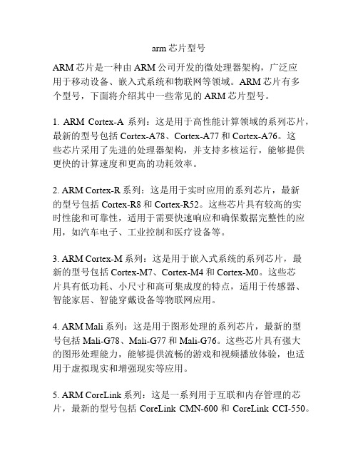
Cortex-A53处理器简介The Cortex-A53 processor is ARM's most efficient application processor ever, delivering today's mainstream smartphone experience in a quarter of the power in the respective process nodes.The Cortex-A53 extremely power efficient ARMv8 processor is capable of supporting 32-bit ARMv7 code and 64-bit code in the AArch64 execution state. It delivers more performance at higher power efficiency than the Cortex-A7 processor, and is capable of being deployed as a standalone main applications processor or as a companion to Cortex-A57 in a big.LITTLE processor.The Cortex-A53 processor can be implemented individually or paired with the Cortex-A57 processor in a big.LITTLE configuration for optimum performance, scalability and energy efficiency.图1.Cortex-A53处理器图片为什么选择Cortex-A53处理器Using ARM's big.LITTLE technology the Cortex-A53 processor will efficiently run your connected life. This connected life will notjust be the social media, news and email updates that you receive today, but will also enable devices to be contextually aware and connect to the Internet of things. Contextual awareness is already happening in smartphones today, but with the Cortex-53 processor's ultra efficiency will allow your smartphone to use its sensor information, calendar, contact information and location-based services to provide relevant information.The Cortex-A53 processor∙Ca n deliver the compute power of today’s high-end smartphone, in lowest power and area footprint, enabling all-day batterylife for typical device uses∙Eficiently run legacy ARM 32-bit applications∙Features cache coherent interoperability with ARM Mali family graphics processing units (GPUs) for GPU compute applications ∙Offers optional reliability and scalability features for high-performance enterprise applications∙Connects seamlessly to ARMs interconnect with up to 16 cores configurations with more in the futureCortex-A53处理器性能The Cortex-A53 processor delivers significantly more performance than its predecessors at a higher level of power efficiency, effectively taking the performance of the LITTLE core above that of the Cortex-A9 processor, which defines today's high-end mobile platforms.The performance graph below shows measured results on Cortex-A9 and early Cortex-A7 test platforms. The results are projected to deliver performance in a quad-core configuration on a "rate" benchmark that tests integer and some floating-point performance with a mix of large and medium data sets. These stress the memory system of each CPU andthe L2 cache. The "rate" portion of the benchmark duplicates the same code on the 2nd, 3rd, and 4th CPUs in each system, and measures the delivered aggregate performance. Rate benchmarks like this evaluate the ability of the multi-processing system to handle memory traffic and coherence requirements in a multiprocessing context.图2.The Cortex-A53 is able to deliver more performance than Cortex-A9 systems of comparable speed on this benchmark. The performance graph below shows measure results running various Android benchmarks on dual-core Cortex-A9, dual-core Cortex-A7, and projected results on dual-core Cortex-A53 platforms based on measured uplift vs. Cortex-A7 on similar types of code. The results show that Cortex-A53 delivers comparable but slightly lower performance relative to Cortex-A9 running at the same frequency, while Cortex-A53 delivers higher performance than Cortex-A9 at the same frequency.表1.* Estimated** Provisonal图3. Cortex-A53处理器产品规格Cortex-A53处理器相关产品The Cortex-A53 MPCore processor incorporates a broad range of ARM technology including System IP, Physical IP, and development tools that also provide support. A broad range of SoC and software designsolutions, tools and services from the ARM Connected Community compliment this technology. That provides ARM Partners with a smooth path through the development, verification and production of full function, compelling devices while significantly reducing time-to-market.系统 IPThe ARM interconnect and memory controller IP addresses the critical challenge of efficiently moving and storing data between up to 16 Cortex-A50 MPCore processors, high performance media processors and dynamic memories to optimize the system performance and power consumption of the SoC. The CoreLink system IP enables SoC designers to maximize the utilization of system memory bandwidth and reduce static and dynamic latencies. While the ARM CoreSight technology provides complete on-chip debug and correlated, real-time trace visibility for all cores of the Cortex-A53 MPCore processor, reducing risk and speeding development of high quality multiprocessing software. The new AMBA 4 Cache Coherent Network (CCN) provides Optimum system bandwidth and latency. The CCN provides AMBA 4 AXI Coherency Extensions (ACE) compliant ports for full coherency between multiple Cortex-A53 MPCore processors, better utilizing caches and simplifying software development. This feature is essential for high bandwidth applications including gaming, servers and networking that require clusters of coherent single and multicore processors. Combined with the ARM CoreLink network interconnect and memory controller IP, the CCN increases system performance and power efficiency.物理 IPARM Physical IP Platforms deliver process optimized IP, for best-in-class implementations of the Cortex-A53 processor at 40nm and below.A set of high performance Optimization Packs (POP) containing advanced ARM Physical IP for 28nm technologies supports the Cortex-A53, to enabling rapid development of leadership physical implementations. ARM is also working early to assure a roadmap to20nm optimizations. Optimization packs support ARM’s strategy of offering specifically targeted Physical IP to enable Partners to achieve tuned implementations of ARM cores. ARM is uniquely able to design the optimization packs in parallel with the Cortex-A53 MPCoreprocessor architecture, enabling the processor and physical IP combination to deliver workstation class performance in a mobilepower envelope while facilitating rapid time-to-market.工具支持The ARM Development Suite 5 (DS-5) tool suite fully supports all ARM processors as well as a wide range of third party tools, operating systems and EDA flows. ARM DS-5 software development tools are unique in their ability to provide solutions that take full advantage of the complete ARM technology portfolio. The ARM Development Studio 5 (DS-5) provides a complete range of software tools to create, debug and optimize systems based on the Cortex-A53 MPCore processor. It incorporates the DS-5 Debugger, whose powerful and intuitivegraphical environment enables fast debugging of bare metal, Linux and Android native applications. In addition, its new ARM Streamline Performance Analyzer simplifies the identification of hot spots in software and load balancing between cores. The ARM Compiler, which already includes specific optimizations for the Cortex-A15 MPCore processor, enables early software development before silicon availability and an ARM Versatile Reference Virtual Platform built on ARM Fast Models technology. This Virtual Platform is available for a free 6-month evaluation.图形处理器The Mali family of products combine to provide the complete graphics stack for all embedded graphics needs, enabling device manufacturers and content developers to deliver the highest quality, cutting edge graphics solutions across the broadest range of consumer devices.支持ARM training courses and Active Assist on-site system-design advisory services enable licensees to integrate efficiently the Cortex-A53 MPCore processor into their design to realize maximum system performance with lowest risk and fastest time-to-market.推荐阅读:∙ARM Cortex-A57与Cortex-A53整体概述摘要:新款ARMv8架构ARM Cortex-A50处理器系列产品,进一步扩大ARM在高性能与低功耗领域的领先地位。
arm芯片型号
arm芯片型号ARM芯片是一种由ARM公司开发的微处理器架构,广泛应用于移动设备、嵌入式系统和物联网等领域。
ARM芯片有多个型号,下面将介绍其中一些常见的ARM芯片型号。
1. ARM Cortex-A系列:这是用于高性能计算领域的系列芯片,最新的型号包括Cortex-A78、Cortex-A77和Cortex-A76。
这些芯片采用了先进的处理器架构,并支持多核运行,能够提供更快的计算速度和更高的功耗效率。
2. ARM Cortex-R系列:这是用于实时应用的系列芯片,最新的型号包括Cortex-R8和Cortex-R52。
这些芯片具有较高的实时性能和可靠性,适用于需要快速响应和确保数据完整性的应用,如汽车电子、工业控制和医疗设备等。
3. ARM Cortex-M系列:这是用于嵌入式系统的系列芯片,最新的型号包括Cortex-M7、Cortex-M4和Cortex-M0。
这些芯片具有低功耗、小尺寸和高可集成度的特点,适用于传感器、智能家居、智能穿戴设备等物联网应用。
4. ARM Mali系列:这是用于图形处理的系列芯片,最新的型号包括Mali-G78、Mali-G77和Mali-G76。
这些芯片具有强大的图形处理能力,能够提供流畅的游戏和视频播放体验,也适用于虚拟现实和增强现实等应用。
5. ARM CoreLink系列:这是一系列用于互联和内存管理的芯片,最新的型号包括CoreLink CMN-600和CoreLink CCI-550。
这些芯片能够提供高性能、高带宽的互联和内存管理能力,支持复杂的系统设计和多核处理。
6. ARM Neoverse系列:这是一系列针对数据中心和网络设备的芯片,最新的型号包括Neoverse N1和Neoverse E1。
这些芯片具有优化的架构和专用的扩展指令集,能够提供低延迟、高吞吐量的数据处理能力。
除了以上的型号,ARM还根据不同的市场需求和应用领域推出了其他系列的芯片,如安全芯片、无线通信芯片等。
主流arm芯片
主流arm芯片ARM(Advanced RISC Machine)是一种基于RISC(Reduced Instruction Set Computer)架构的芯片设计,它广泛应用于移动设备、嵌入式系统和智能物联网等领域。
本文将重点介绍几款主流的ARM芯片,包括ARM Cortex-A系列和ARMCortex-M系列。
首先,ARM Cortex-A系列芯片是专为高性能应用而设计的。
其中最著名的是Cortex-A76,它是ARM的第四代高性能CPU,采用了7纳米制程工艺,在性能和功耗方面取得了显著的突破。
Cortex-A76具有三级流水线架构,支持超标量和超流水线技术,能够实现更高的指令并行度。
此外,Cortex-A76还引入了ARM的动态预测技术,能够对程序的分支进行智能预测,提高指令的执行效率。
Cortex-A76还支持硬件加速器,如浮点单位和向量浮点单位,使其在处理复杂的图形和计算任务时表现出色。
其次,ARM Cortex-M系列芯片是专为低功耗和实时应用而设计的。
其中最新的一款芯片是Cortex-M33,它采用了22纳米制程工艺,拥有强大的处理能力和低功耗特性。
Cortex-M33支持ARM的TrustZone技术,可以实现硬件级别的安全隔离,保护敏感数据免受恶意攻击。
此外,Cortex-M33还具有较高的实时性能,可以满足实时控制和物联网应用的需求。
与此同时,Cortex-M33还具有较低的功耗,可以延长设备的电池寿命。
另外,ARM还推出了一系列专用的图形处理器(GPU)芯片,用于处理图形和媒体内容。
其中比较著名的是Mali系列GPU 芯片,如Mali-G76和Mali-G77。
这些芯片采用了先进的图形处理架构,支持高清视频解码和3D图形渲染。
Mali-G76是一款面向高性能移动设备的高性能GPU芯片,可以提供流畅的游戏和多媒体体验。
而Mali-G77是一款面向VR和AR设备的高性能GPU芯片,具有更高的计算能力和更低的功耗。
arm cortex-m3全可编程soc原理
arm cortex-m3全可编程soc原理如下:
1.架构:Cortex-M3 核心是基于ARMv7-M 架构,这是一个针对
嵌入式应用程序优化的架构。
它包含一个ARM 指令集、一个
ARM 连接至程序的接口以及一些特定于嵌入式应用的扩展。
2.核心功能:Cortex-M3 核心具有高性能、低功耗和低成本的特
点。
它包含一个32 位RISC 处理器,具有一个三级流水线。
核心还包含一个嵌套向量中断控制器,允许高效的异常和中断
处理。
3.可编程性:Cortex-M3 是完全可编程的。
这意味着硬件和软件
都可以通过编程来定制。
ARM 的微控制器工具链(如Keil 或
IAR)可用于编译和调试代码,以适应特定的应用需求。
4.系统集成:SoC 是一种将多个硬件组件集成到一个单一芯片上
的技术。
在Cortex-M3 中,这些组件可能包括内存、通信接口、
ADC、DAC 等。
通过将所有这些组件集成到单个芯片上,可以
降低系统成本、减小体积并提高可靠性。
5.低功耗:Cortex-M3 被设计为低功耗微控制器,适用于电池供
电的应用。
它具有多种低功耗模式,可以在不使用时降低功耗。
6.安全性:Cortex-M3 提供了多种安全特性,如内存保护单元
(MPU)和安全区域(Secure Zone),以保护敏感数据和代码。
浅谈ARM-Cortex系列处理器之区别
浅谈ARM Cortex系列处理器之区别市面上ARM Cortex系列包括3个系列,包括ARM Cortex-A,ARM Cortex—R,ARM Cortex —M,Z这三种系列,并且每个系列又分多种子版本,每个子版本都有各自的特点。
很好的为设计人员提供非常广泛的具有可扩展性的性能选项,从而有机会在多种选项中选择最适合自身应用的内核,而非千篇一律的采用同一方案.其中,1,Cortex-A-面向性能密集型系统的应用处理器内核2, Cortex-R-面向实时应用的高性能内核3, Cortex-M-面向各类嵌入式应用的微控制器内核Cortex-A处理器为利用操作系统(例如Linux或者Android ,IOS)的设备提供了一系列解决方案,这些设备被用于各类应用,从低成本手持设备到智能手机、平板电脑、机顶盒以及企业网络设备等。
早期的Cortex-A系列处理器(A5、A7、A8、A9、A12、A15和A17)基于ARMv7-A架构。
每种内核都共享相同的功能集,例如NEON媒体处理引擎、Trustzone安全扩展、单精度和双精度浮点支持、以及对多种指令集(ARM、Thumb—2、Thumb、Jazelle 和DSP)的支持。
与此同时,这些处理器也具有极高的设计灵活性,能够提供所需的最佳性能和预期的功效.介绍过Cortex-A,下面介绍Cortex—R系列——衍生产品中体积最小的ARM处理器,这一点也最不为人所知。
Cortex—R处理器针对高性能实时应用,例如硬盘控制器(或固态驱动控制器)、企业中的网络设备和打印机、消费电子设备(例如蓝光播放器和媒体播放器)、以及汽车应用(例如安全气囊、制动系统和发动机管理)。
Cortex—R系列在某些方面与高端微控制器(MCU)类似,但是,针对的是比通常使用标准MCU的系统还要大型的系统。
例如,Cortex-R4就非常适合汽车应用.Cortex—R4主频可以高达600MHz(具有2。
ARM Cortex-M3 内核介绍
ARM Cortex-M3 内核介绍内核包含四部分:1.乘法器;2.控制逻辑;3.Thumb 指令译码器;4.内部接口CM3 内部包含元素介绍:1. DAP,调试访问接口,Debug Access Port。
Cortex‐M3 的调试系统基于ARM 最新的CoreSight 架构。
不同于以往的ARM 处理器,内核本身不再含有JTAG 接口。
取而代之的,是CPU 提供称为调试访问接口(DAP)的总线接口。
通过这个总线接口,可以访问芯片的寄存器,也可以访问系统存储器,甚至是在内核运行的时候访问!对此总线接口的使用,是由一个调试端口(DP)设备完成的。
DPs 不属于CM3 内核,但它们是在芯片的内部实现的。
目前可用的DPs 包括SWJ‐DP(既支持传统的JTAG 调试,也支持新的串行线调试协议),另一个SW‐DP 则去掉了对JTAG 的支持。
另外,也可以使用ARM CoreSignt 产品家族的JTAG‐DP 模块。
这下就有 3 个DPs 可以选了,芯片制造商可以从中选择一个,以提供具体的调试接口(通常都是选SWJ‐DP)。
2. ETM 的作用就是记录处理器做的事情并送到外面的调试器。
由于微控制器带有大量的片内存储器,因此不能简单地通过观察外部管脚来确定处理器核是如何运行的。
ETM 对深嵌入处理器内核提供了实时跟踪能力。
它向一个跟踪端口输出处理器执行的信息。
软件调试器允许使用JTAG 接口对ETM 进行配置并以用户易于理解的格式显示捕获到的跟踪信息。
ETM 直接连接到ARM 内核而不是主AMBA 系统总线。
3.NVIC 是Cortex-M3 处理器中一个完整的部分,它可以进行高度配置,为处理器提供出色的中断处理能力。
在NVIC 的标准执行中,它提供了一个非屏蔽中断(NMI)和32 个通用物理中断,这些中断带有8 级的抢占优先权。
NVIC可以通过综合选择配置为1 到240 个物理中断中的任何一个,并带有多达256。
- 1、下载文档前请自行甄别文档内容的完整性,平台不提供额外的编辑、内容补充、找答案等附加服务。
- 2、"仅部分预览"的文档,不可在线预览部分如存在完整性等问题,可反馈申请退款(可完整预览的文档不适用该条件!)。
- 3、如文档侵犯您的权益,请联系客服反馈,我们会尽快为您处理(人工客服工作时间:9:00-18:30)。
ARM Cortex处理器: 新一代高性能、低功耗 嵌入式系统的最佳选择罗霖 ARM 中国嵌入式业务开发经理 2009年4月9日,深圳1提纲1. 2. 3. 4.知识产权发展对集成电路和嵌入式系统的影响后PC时代-嵌入式的到来!ARM的技术及发展路线新一代高性能、低功耗处理器Cortex-A8x1-4Cortex-A9嵌入式开发的市场机遇如何在有限功耗实现高性能Cortex-R4 Cortex-R4F未来嵌入式开发的挑战软件的复杂性及平台化开发Cortex-M3 SC300™Cortex-M1 & M02消费者身边日益增多的数字产品Driving forces Performance requirements and time§ Digitisation § New applications § New uses § New value § New economiesTime à 25+ Years3逐渐“隐藏” 的嵌入式技术2006 Chrysler announce 40% of models will offer iPod integration2015 - Pervasive but hidden electronics1913 Model T Ford No electronicsCirca 1980 BMW 733i Introduction of ABS 2005 BMW 7 Series iDrive Control system4不断提高的性能(计算、通信、图形、用户界面)§ Increased performance andfunctional integration § Multiple processors § Multiple software layers § Very high gate counts § Mixed signal § Platform cost put at $1B**Gartner, February 2006 /ace/jbench/loginARM9 ARM7 ARM9 ARM11 ARM7ARM115今天:一个“崭新”的半导体产业Cost of 1MHz Cost of 1 Megabit storage Cost of sending 1 trillion bits1970 1980 $7,600.82 $103.40 $5,256.90 $614.40 $150,000.00 $129,166.671990 $25.47 $7.85 $90.422002 $0.17 $0.33 $0.12Source: “The New Paradigm” Federal Reserve Bank of Dallas 1999 Report and 2002 Actuals6ARM商业模式: 知识产权(IP)授权ARM 开发用于设计 和完成芯片的技术 ARM 在软件和 工具领域进行投入SoC SoC memory memory从2001年开始 持续9亿美金ARM 把IP授权给 主要的芯片厂商OEM厂商能够开发多种低成本及差异化 的产品 OEM厂商能够从 不同的供应商那 采购到软件互相 兼容的芯片产品7ARM的创新技术开发社区 开发工具 软件 IP处理器 系统级 IP: 数字引擎 结构 3D 图形 视频 物理 IPSoCmemory8知识产权业务模式的经济效益§Outsource R&DRelative Implementation Cost11 10 9 8 7 6 5 4 3 2 1§ §Reduces up-front design costs ARM has invested $900M in R&D since 2001 and created ARM11 and Cortex families13 stage8 stage 6 stage§ § § §72 ARM11 licenses 56 Cortex licenses5 stage 3 stageCore Performance and ComplexityWould have cost industry more than $16Bn to create equivalent product portfolios Adding delay and risk without differentiationRelative Complexity300 250 200 150§IP cost-sharing business model is required for a mature industry to remain profitable100 50 0250nm 180nm 130nm90nm65nm45nm32nm9知识产权业务模式促进差异化创新及市场增长1997 ARM and Partners Enabling 2007 4 Bn Users 3 Bn (2009) Users1Ecosystem Delivering Low Power Today Diverse Range of Products Rapidly Growing MarketsIntel Platforms have only driven size and speed How much has your laptop changed over the years ?1 21 Bn Users2Strategy Analytics 2007 Innovations: Costs + Risks + Time to Market102009年:今天的ARM§业界领先的硅知识产权公司§ §领先的32 bit RISC 体系架构 § 累计出货140亿ARM处理器 全球每人两个ARM 领先的物理知识产权§§ 每年1500新项目基于ARM的标准单元§ § §2008年: 40亿个 ARM处理器出货 § Now 1 Billion ARM Processors shipments each Quarter 全球1700位员工, 32 个地区办公室 2008年:全球四分之一的电子产品是由我们的合作伙伴提供的并基于ARM 的技术。
112. ARM的技术及发展路线12ARM公司的远景ARM designs technology that lies at the heart of advanced digital products13ARM Cortex 系列处理器Bringing the benefits of architectural innovation across the computing spectrum§ARM Cortex™-A Series:§Applications processors for complex OS and user applicationsCortex-A8x1-4Cortex-A9§ARM Cortex-R Series:§Embedded processors for real-time signal processing and control applicationsCortex-R4 Cortex-R4F§ARM Cortex-M Series:§Deeply embedded processors optimized for microcontroller and low-power applicationsCortex-M3 SC300™ Cortex-M114满足不同需求的ARM处理器Cortex-A9 Cortex-A8 ARM11™ MPCore™ ARM1176J(F)-S™ ARM926EJ-S™ 4X 4XApplicationsCortex-R4(F) ARM1156T2(F)-S™ ARM946E-S™ ARM968E-S™ ARM7TDMI®Cortex-R4XReal-Time EmbeddedCortex-M3 Cortex-M1 ARM7TDMIMCU & FPGA15应用处理器的技术路线§ Application compatibility across multiplegenerations of processorsARMv7-Cortexx1-4Cortex-A9 Cortex-A8ARMv6x1-4§ Driven by power efficiencyand scalable performanceARM11 MPCore ARM1176JZ(F)-S ARM1136J(F)-S§ Ideal processor forsupporting high level OSARMv5ARM1026EJ-S ARM926EJ-SARMv4ARM920T ARM922T16Cortex-A8 处理器介绍§ Highest performance Cortex-A processor provenin silicon mass production today§ § § § § §Superscalar pipeline delivers 2 DMIPS/MHz Thumb-2 ISA for performance and code density TrustZone extensions for secure transactions and DRM NEON multimedia and signal processing unit delivers over 2x performance of ARMv6 SIMD Integrated L2 Cache with configurable size and ECC§ Maximum implementation flexibility§ § § §Synthesizable RTL –or– Optimized with customs Same verilog code base65nm LP process 65nm G+ process Optimized Advantage-CE Custom Synthesized Advantage-HS Advantage**PPAStandard Cells Memories Frequency (MHz) Area with cache (mm2)Optimized Advantage-CE CustomSynthesized Advantage-HS Advantage**§ Ecosystem in placeTools Middleware OS support660-700 3.86 2.79 32K/32K 0.58 -500-550 4.2 3.1 32K/32K 0.75 -1.1 GHz+ 3.86 2.79 32K/32K 0.43 -800+ 4.2 3.1 32K/32K 0.55 -Area without cache (mm2) Cache size Power with cache (mW/MHz) Power w/o cache (mW/MHz)** Optimized instances of Advantage RAMS Area includes L1 RAMS, L2 control. Excludes NEON, ETM, L2 RAMS17Cortex-A9处理器介绍 § Optimized Cortex-A processor enabling breakthroughperformance and power scalability§ § § § §2nd generation 1-4X SMP technology Delivered as Uniprocessor and 1-4X MP Advanced pipeline delivering ~25% more DMIPS/MHz over Cortex-A8 (2.5) Comparable FMAX to fully synthesized Cortex-A8 in same configuration Optimized floating-point unit; NEON engine§ New system-level integration§ § §features for design optimizationAccelerator coherence port Advanced bus interface unit for maximum throughput Generalized interrupt control and distribution system“Symbian and ARM Cooperate in Bringing Symmetric Multi Processing (SMP) to Future Phones Enabling High-End PC Capabilities to Consumers’ Pockets”– 10/07§ Suitable for high-end enterprisenetworking through to wireless handsets18嵌入处理器的技术路线§ Industry standard, proven technology § Cost effective, power-efficient performance § Leadership softwareARMv6 ARMv7-CortexCortex-R4F Cortex-R4compatibility§ Widest choice ofembedded OSARMv5ARM1156T2(F)-SARM1026EJ-S ARM968E-S ARM966E-S SC200 Cortex-M3ARM946E-S ARM7EJ-SARMv4SC300ARM7TDMI(S)SC100Cortex-M119Cortex-R4(F) 处理器介绍 § High-performance processor optimized for deeplyembedded signal-processing and control applications§ § § §8-stage superscalar pipeline delivers up to 400MHz+ @ 1.6DMIPS/MHz on 90nm Thumb®-2 technology, hardware divide State-of-the-art ECC support in all memories AMBA 3 AXI slave port for DMA to TCMs§ Fit-for-purpose configurability§ § § § § § §Separately configured L1 caches: 0kB, 4-64kB 0 to 3 TCMs of up to 8MB each 8 or 12 regions in MPU, or no MPU 2 – 8 Breakpoints, 1 – 8 Watchpoints Parity or ECC can be optionally included Optional SP-optimised FPU (full IEEE754) Optional slave port20§An ARM7TDMI-S for the 21stcentury§For extreme cost and power-sensitive complex applications §Comparable or better F MAX and gate count with r2p0 min config §30% more DMIPS, 28% more geomean EEMBC §85% more DMIPS per mW §State-of-the-art functionality§Code everything in C§Thumb-2 ISA → 6X code density, 10X perf. v 8051§Integrated Nested Vectored Interrupt Controller (NVIC) with lowest interrupt latency of any ARM§Configurable/optional memory protection, debug, trace §uA device stand-by enabled with integrated sleep modes,ULL libraries, state retention§Broad adoption within Microcontroller industry“…. the Cortex-M3 processor will propel us againtowards a breakthrough in performance, ease ofuse and quality, while also providing acompetitive cost structure for our products. We feel that the Cortex M3 processor will play an important role in accelerating the convergence of the MCU market …”–Jim Nicholas, GM Microcontroller Division, ST§First ARM processor specifically optimized for FPGA §High frequency, low-area soft processor for low-cost volume FPGA§Upwards compatible with Cortex-M3 onwards on ASIC/ASSP/MCU§Capable of up to 200MHz on fast FPGA device§Delivers up to 0.8 DMIPS/MHz efficiency from TCM§Designed for synthesis on multiple FPGA types §Actel ProASIC3, Actel Igloo and Actel Fusion§Altera Cyclone-III, Altera Stratix-III§Xilinx Spartan-3, Xilinx Virtex-5§3 Channels to market§Traditional ARM licensing§NEW: Altera/Arrow 1X design start§NEW: Freely available to Actel usersARM推出体积最小、能耗最低、最节能的处理器Cortex-M0处理器以8位处理器的价位提供32位处理器的性能,并兼容诸如Cortex-M3产品的多功能处理器Enabling the next 10+ billion units from under $1 to over 1GHzM i l l i o n s o f D o l l a r s2001200220032004200520062007200820092010201132-Bit +16-Bit8-Bit4-BitCortex-M 系列处理器加速ARM MCU 市场的发展Source: Semico 1Q07•32-bit taking 8/16-bit socketsCortex-M0 和Cortex-M3 处理器§Cortex-M3 processor is ARM’s flagship Cortex-M class processor §Offering superior efficiency and flexibility§Cortex-M0 processor is an ultra low-power, streamlined subset of Cortex-M3 processor§With easy migration to the Cortex-M3 processor§Coherent architecture spanning cost/performance points Comparison Cortex-M0Cortex-M3DMIPS/MHz0.9 1.25Energy efficiency DMIPS/mW6031Gate count 12k48kArea 0.25 mm20.68 mm2 Number interrupts1-32 + NMI1-240 + NMI Interrupt priorities4256 Breakpoints, Watchpoints4/2, 2/18/4, 2/1 MPU, integrated trace option No Yes Hardware Divide NoYes0.20.40.60.811.21.4ARM7(Thumb)Cortex-M0ARM7(ARM)Cortex-M3 Relative DMIPS/MHz超低的功耗Ultra Low Power§Designed for low per MHz power§Just 15 μW/MHz (90G Advantage implementation)§Delivering exceptional 60 DMIPS/mW efficiency§Architected for ultra low power deep sleep§Excellent static power results using Metro ™180ULL libraries §Processor supports latest State Retention flow using ARM PMK§Easy integration to power management unit via Wake-up Interrupt Controller§Never change the battery!§Using a standard 230mAh lithium cell§For example a ZigBee node -0.1% activity at 10MHz §This gives 30 years of battery life<50 nADeep sleepWith state retention150 nAStandbyProcessor clock gatedArtisan Metro 180ULL “Cortex-M0” prototype implementation80 μAActive (Dhrystone 2.1)Per MHz优秀的效率Excellent Performance Efficiency §Superior per cycle performance to 16-bit devices §Lower MHz, shorter active duty cycles, longer battery life智能传感器§Sensor elements that capture analog data§Temperature, Voltage, Pressure, Acceleration§The sensor is combined with digital logic§Pre-process the results for example to filter or resample §Transmit the results to another device§Cortex-M0 is designed to perform these digital tasks§Sensors can have multiple uses§E.g automotive accelerometers used in airbags and stability controlAn absolute pressure sensor that usesMEMS technologyInertial Measurement Unit (IMU), single chip triple axisaccelerometer and three iMEMs gyroscopes to provide Roll, Pitch, and Yaw3. 嵌入式开发的市场机遇“酷”的产品Cool ProductsSamsung SMT-H30560 Cable STB Conexant CX2417X –ARM920T ProcessorSonosite MTurbo (Portable Ultrasound Device)Texas Instruments TMS320DM644x -ARM926 ProcessoriRiver Unit 2 Multimedia Home Networking device Telechips and Samsung –ARM9E + ARM11 ProcessorsSunlink International -SunView PMP + ProjectorSamsung S3C244A –ARM9 ProcessorD-Link DNS323 Network Storage Enclosure Marvell 88F5181 Soc –ARM9 processorInnovations for learning -TeachermateARM9 ProcessorEmbedded Automation –mPanel (Digital Home Device)ARM architecture-based –Marvel XScaleBlackberry Bold Marvell "Tavor" PXA930ARM Architecture Based –Xscale processoriRiver NV Life PMP Magic Eyes -ARM926EJ +ARM946EEverex Cloudbook UMPCGCT Semiconductor –ARM9 ProcessorImportek Apollo VoIP Video PhoneARM9 + Marvell Xscale processorArtega -Artega GT (Dual-Dashboard Display)Fujitsu MB86R01 "Jade" graphics controllerARM926EJ-s +Jazelle Java Acceleration TechnologyGarmin Nuvi 205ST Cartesio Processor -ARM926Thomson WiFi TabletTI DaVinci TMS320DM6441 –ARM926EJ-SCustom Engineering -TK300II Desktop Ticket PrinterARM Processor (266MHz)VivoPay –Vivo KioskARM Powered基于ARM的应用BasicWeb2.0 PhoneNetbook FeaturePhone基于ARM的DTV / STB / BD 方案STB DTV BluRayCPU ARM11 /Cortex-A8; Cortex-A9ARM11 /Cortex-A8; Cortex-A9Cortex-A8; Cortex-A9Memory128-512MB128-256MB1GB+ GraphicsGPUMali-200 / Mali-400 MP2/3D Graphics Mali-200 / Mali-400 MPVideo Dual SD/HD Multi-stddecode SD/HD Multi-std decodeDual SD/HD Multi-std decodeAudio Software Software Software Java For Tru2Way / MHP boxes Tru2Way Required (CDC) Internet/BrowserSome Some Required (profile 2.0)未来的家庭及企业网络应用未来的机会: 不受“线”制的移动计算Classic PC–hours of useDelivering Web browsing and emailUsing a fraction of the power MIDsSmartphonesARM technology delivers days-of-use in UltraportablesAdding ARM sub-system gives days-of-useF r e e d o m !Days of useF r e q u e n t R e c h a r g i n g低功耗:全天使用的前提§All Day Use Model§Differentiation§Low thermal requirements enables freedom of industrial design §Select the “best in class ” SoCs from ARM ’s partners §Multiple suppliers drives competition and innovation§ARM based SoCs enable BOMs < Intel Atom based systems §Wireless communication is designed in, not an after thoughtEstimates for ultraportable notebook with 2200 mAh battery9.4 Hours 3.1 Hours 6.3 Hours 1.6 Hours3x longer web surfingFull day useWeb Surfing ARM Cortex-A8Video Playback ARM Cortex-A8Web Surfing Intel Atom Video PlaybackIntel AtomGreater than 3x video enjoyment ¾ HD compared to 3 HD moviesLow Power =Great User Experience§Usability -Average Power§Consumers want to be Mobile§Cortex-A8 delivers days-of-use, not hours§Sleep§Cortex-A8 saves contents to external DRAM and turns off§Weeks of standby not hours20406080100120140160Sleep Average MilliwattsSleep AverageIntel0.8 days0.4 daysARM Weeks 6.9 daysLife from a 1400mAh BatteryProcessor Core Only移动应用:电池寿命是关键•ARM Cortex-A8 projections use the same statistical distribution of power states as Intel Atom.•Average use assumes following power state distribution-C0: 5%,C1-C4:15%, C6: 80%•Projections for core only at 800 MHz. Days calculated on 24hr clock.•Intel Z500 (C0-C6) state power state estimates from Intel datasheet (319535-001US). Averagepower estimates based on Microprocessor Report article “Intel’s tiny ATOM”.性能比较: Cortex-A8 & Atom §Quick “on a napkin” analysis ofIntel performance claims§ARM11 @ 400MHz with no L2§800 MHz Intel® Atom™ with512KB L2§ 1.6 GHz Atom with 512KB L2§“Apples to Apples”§2X --Double the Frequency from400 MHz to 800 MHz§~2.5X –No L2 to 128KB L2§~1.8X –Architectureimprovement from ARM11 toCortex-A8=5101520253035Ford Web SiteRuntime(Seconds)Intel® Atom™Z530 1.6GHzIntel AtomZ510 800MHzARM11 400 MHzDouble Frequency400 to 800 MHzAdd 128KB L2,no L2 beforeARM11 to Cortex-A8ArchitectureImprovementPerformance Estimates OnWebpage Reader(Network Dependencies Removed)Smaller is betterIntel benchmark numbers from Intel FallIDF ’08 Taiwan presentation given byAnand Chandrasekhar基于ARM的方案3D Graphics HD Video Radios Linux Window Mobile Android Window EmbeddedCompanyProductCoreSpeedNVIDIA Samsung SamsungTegra™ 610 6410 S5PC100ARM11 MPCore™ ARM11 Cortex-A8 V7 Architecture License Cortex-A8 Cortex-A8 Cortex-A9 V5 Architecture License800 MHz 667 MHz 800MHzX X XX SD X X X XX X XX X XQualcomm Freescale TI TISnapDragon™ iMX515 OMAP™ 3 OMAP™4 PXA3## (contact for all the products)1 GHz 1 GHz 1 GHz 2 cores, 1GHz ea 803 MHzX X X XX X X XXX XX X X XX X X XX XX XMarvellXSDXXXXMID/Hybrid 2009 2010V7 – Cortex-A8, minimum 256MB, start of integrated radios and GPS V7 – Cortex-A8 and Cortex-A9, minimum 512MB, highly integrated and cost reduced solutions … radios, GPS, accelerometersNetbookV7 – Cortex-A8 and first Cortex-A9, minimum 512MB V7 – Mix of single and multi-core, multi GB memory, start of integration for cost reduction41移动计算 OS 的选择Product“Smartphone”Operating SystemsSymbian Windows Mobile Linux - Various Windows Embedded“MID”PMP, PND, Internet TabletLinux – Android Linux (various flavors)Ultraportable Notebook HybridARM for browsing, email, multimedia X86 when needed > 15 hr useUbuntu – Canonical Big Windows - TBD Windows Embedded Linux – 42Web 2.0 ARM的生态系统New ProgramsMozilla Fennec Adobe Flash Player10 and AIR Official release of Mozilla browser for mobile Fennec (FF3 engine) is expected end Q1’09 Optimizations for ARMv6 and ARMv7, 2H 2009 Support for GPUs & HW through open standards (OpenGL-ES 2.0) Targeting Nokia S60 & WM6.x, 1H 2009 Silverlight Support for ARM Java Standard Edition for ARM Live Mesh on ARM ARMv6 is minimum required, we expect support for OpenGL-ES 2.0 also. .NET is app framework Targeting Java Standard Edition v6.10 to ARM Early access release expected in Q1 2009 Device data synchronization, mixes with Silverlight for rich cloud applications Beta released on Windows Mobile at PDC 2008.434. 未来嵌入式开发的挑战44未来的移动芯片:复杂的硬件集成§ARM typically supplies: § The processor subsystem § How fast facebook opens § Whether Flash10 content is possible § What type of games can be played § Responsiveness of UI § Battery life § The graphics processor & software § Desktop quality graphics § “Coverflow” type interfaces § Gaming experience § Fast panning, zooming, flipping § Battery lifeEDGE uC DDR2 Proc Fabric L2 & 3G Periph Cache RAM Audio DSP GPU RAM LTE USB/ Video MIPIProcessor & graphics affect: Services User experience OEM/Operator ARPU45不断上升的软件集成费用§ High-performance devicesrun large amounts of complex software§ All needs to be developedand integrated into final device12846今天的现实:来自复杂的软件挑战54% 66%Device software designs are completed behind schedule“2003 Embedded Development Tools & RTOSes,” EMF, June 2003Device software designs are completed over budget“2003 Embedded Software Study,” DDC, September 200333%Produced devices do not meet performance or functionality requirements“2003 Embedded Development Tools & RTOSes,” EMF, June 200314 BillionDevices will be connected in 5 years“X Internet” Reports, 2001-2003Source: WindRiver47为什么要关心CPU?SW SW SWLegacy code across all company products§For each additional toolchain: § IT Costs $$ § Reliability A consistent CPU architecture enables software and toolchain reuseToolchain16-bit 8-bit32-bit§§ What would happen in the computer software industry if.. § Every new PC used a different CPU architecture § You had to maintain different compilers for every new PC § Common architecture can make Embedded Software reusea reality48ARM技术授权的软件优势SW SW SWLegacy code across all company productsToolchainMicrocontrollers FPGA’sApplications processors, System-on-Chip etc.§ Enabling a standard platform for embedded development § Protecting investment in software design § Forget traditional 8/16/32-bit perceptions, think of it as a §‘Software Engine’ Enable reuse, not just from MCU to MCU but onto other digital solutions49中国低成本创新的新阶段Branding R&D Branding R&DDesigning Engineering DistributionDesigning Engineering DistributionManufacturingManufacturing1990s2000sZeng & Williamson (2008)50。