DS18B20 数字温度计外文资料翻译
机械毕业设计英文外文翻译8DS18B20的研究与应用
附录Research and Application of DS18B20Communication to the DS18B20 is via a 1-Wire port. With the 1-Wire port, the memory and control functions will not be available before the ROM function protocol has been established. The master must first provide one of five ROM function commands: 1) Read ROM, 2) Match ROM, 3) Search ROM, 4) Skip ROM, or 5) Alarm Search. These commands operate on the 64-bit lasered ROM portion of each device and can single out a specific device if many are present on the 1-Wire line as well as indicate to the bus master how many and what types of devices are present. After a ROM function sequence has been successfully executed, the memory and control functions are accessible and the master may then provide any one of the six memory and control function commands.One control function command instructs the DS18B20 to perform a temperature measurement. The result of this measurement will be placed in the DS18B20’s scr atch-pad memory, and may be read by issuing a memory function command which reads the contents of the scratchpad memory. The temperature alarm triggers TH and TL consist of 1 byte EEPROM each. If the alarm search command is not applied to the DS18B20, theseregisters may be used as general purpose user memory. The scratchpad also contains a configuration byte to set the desired resolution of the temperature to digital conversion. Writing TH, TL, and the configuration byte is done using a memory function command. Read access to these registers is through the scratchpad. All data is read and written least significant bit first.In order for the DS18B20 to be able to perform accurate temperature conversions, sufficient power must be provided over the DQ line when a temperature conversion is taking place. Since the operating current of the DS18B20 is up to 1.5 mA, the DQ line will not have sufficient drive due to the 5k pullup resistor. This problem is particularly acute if several DS18B20s are on the same DQ and attempting to convert simultaneously.There are two ways to assure that the DS18B20 has sufficient supply current during its active conversion cycle. The first is to provide a strong pullup on the DQ line whenever temperature conversions or copies to the E2 memory are taking place. This may be accomplished by using a MOSFET to pull the DQ line directly to the power supply as shown in Figure 2. The DQ line must beissuing any protocol that involves copying to the E2 memory or initiates temperature conversions. When using the parasite powermode, the VDD pin must be tied to ground.Another method of supplying current to the DS18B20 is through the use of an external power supply tied to the VDD pin. The advantage to this is that the strong pullup is not required on the DQ line, and the bus master need not be tied up holding that line high during temperature conversions.This allows other data traffic on the 1-Wire bus during the conversion time. In addition, any number of DS18B20s may be placed on the 1-Wire bus, and if they all use external power, they may all simultaneously perform temperature conversions by issuing the Skip ROM command and then issuing the Convert T command. Note that as long as the external power supply is active, the GND pin may not be floating.The core functionality of the DS18B20 is its direct-to-digital temperature sensor. The resolution of the DS18B20 is configurable (9, 10, 11, or 12 bits), with 12-bit readings the factory default state.command, a temperature conversion is performed and the thermal data is stored in the scratchpad memory in a 16-bit, sign-extended two’s complement format. The temperature information can be retrieved over the 1-Wire interface by issuing a Read Scratchpad [BEh] command once the conversion has been performed. The datais transferred over the 1-Wire bus, LSB first. The MSB of the temperature register contains the “sign” (S) bit, denoting whether the temperature is positive or negative.Each DS18B20 contains a unique ROM code that is 64-bits long. The first 8 bits are a 1-Wire family code (DS18B20 code is 28h). The next 48 bits are a unique serial number. The last 8 bits are a CRC of the first 56 bits. The 64-bit ROM and ROM Function Control section allow the DS18B20 to operate as a 1-Wire device and follow the 1-Wire protocol detailed in the section “1-Wire Bus System.” The functions required to control sections of the DS18B20 are not accessible until the ROM function protocol has been satisfied. This protocol is described in the ROM function protocol flowchart. The 1-Wire bus master must first provide one of five ROM function commands: 1) Read ROM, 2) Match ROM, 3) Search ROM, 4) Skip ROM, or 5) Alarm Search. After a ROM function sequence has been successfully executed, the functions specific to the DS18B20 are accessible and the bus master may then provide one of the six memory and control function commands.The DS18B20 has an 8-bit CRC stored in the most significant byte of the 64-bit ROM. The bus master can compute a CRC value from the first 56-bits of the 64-bit ROM and compare it to the value stored within the DS18B20 to determine if the ROM data has beenreceived error-free by the bus master. The equivalent polynomial function of this CRC is:CRC = X8 + X5 + X4 + 1The DS18B20 also generates an 8-bit CRC value using the same polynomial function shown above and provides this value to the bus master to validate the transfer of data bytes. In each case where a CRC is used for data transfer validation, the bus master must calculate a CRC value using the polynomial function given above and compare the calculated value to either the 8-bit CRC value stored in the 64-bitROM portion of the DS18B20 (for ROM reads) or the 8-bit CRC value computed within the DS18B20(which is read as a ninth byte when the scratchpad is read). The comparison of CRC values and decision to continue with an operation are determined entirely by the bus master. There is no circuitry inside the DS18B20 that prevents a command sequence from proceeding if the CRC stored in or calculated by the DS18B20 does not match the value generated by the bus master.The scratchpad is organized as eight bytes of memory. The first 2 bytes contain the LSB and the MSB of the measured temperature information, respectively. The third and fourth bytes are volatile copies of TH and TL and are refreshed with every power-on reset.The fifth byte is a volatile copy of the configuration register and is refreshed with every power-on reset. The configuration register will be explained in more detail later in this section of the datasheet. The sixth, seventh, and eighth bytes are used for internal computations, and thus will not read out any predictable pattern.It is imperative that one writes TH, TL, and config in succession;i.e. a write is not valid if one writes only to TH and TL, for example, and then issues a reset. If any of these bytes must be written, all three must be written before a reset is issued.There is a ninth byte which may be read with a Read Scratchpad [BEh] command. This byte contains a cyclic redundancy check (CRC) byte which is the CRC over all of the eight previous bytes. This CRC is implemented in the fashion described in the section titled “CRC Generation”.DS18B20的研究与应用DS18B20的通信是通过一个1 - Wire端口。
温度传感器DS18B20_外文翻译
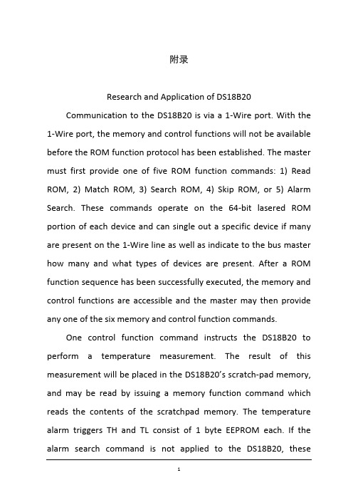
DS18B20Programmable Resolution1-WireDigital Thermometer1、DS18B20FEATURES(1)Unique1-Wire interface requires only one Port pin for communication,requires no external components(2)Each device has a unique64-bit serial code stored in an onboard ROM(3)Can be powered form data line.Power supply range is3.0Vto5.5V(4)Measures temperatures form-55℃to+125℃,±0.5℃accuracy from-10℃to +85℃(5)Thermometer resolution is user-selected from9to12bits(6)Converts temperature to12-bit digital word in750ms(max)(7)Alarm search command identifies and addresses devices whose temperature is outside of programmed limits(temperature alarm condition)(8)Available in8-pin SOIC,and3-bin TO-92packages2、DS18B20BLOCK DIAFRAMFigure1shows a block diagram of the DS18B20,The64-bite ROM stores the device’s serial code.The scratchpad memory contains the2-byte temperature egister that stores the digital output from the temperature sensor.In addition,the scratchpad provides access to the1-byte upper and lower alarm trigger register(TH and TL),and the1-byte configuratuion register.The configuration register allows the user to set the resolution of the temperature-to-digital conversion to9,10,11or12bits.The TH,TL and configuration registers are nonvolatile(EEPROM),so they will retain data when the device is powered down.Figure1block diagram of the DS18B203、DS18B20ROM COMMANDS(1)SEARCH ROM[0F0H]When a system is initially powered up,the master must identify the ROM codes of all slave devices on the bus,which allows the master to determine the number of slaves and their device types.The master learns the ROM codes through a process of elimination that requires the master to perform a Search ROM cycle as many times as necessary to identify all of the slave’s64-bit ROM devices.(2)READ ROM[55H]This command can only be used when there is one slave on the bus.It allows the bus master to read the slave`64-bit ROM code without using the Search ROM procedure.If this command is used when there is more than one slave present on the bus,a data collision will occur when all the slaves attempt to respond at the same time.(3)MATCH ROM[55H]The match ROM command followed by a64-bit ROM code sequence allows the bus master to address a specific DS18B20on a multidrop or single-drop bus.Only the DS18B20that exactly matches the64-bitROM code sequence will respond to thefunction command issued by the master;all other slaves on the bus will wait for a reset pulse.(4)SKIP ROM[0CCH]The master can use this command to address all devices on the bus simultaneously without sending out any ROM code information.Note that the Read Scratchpad command can follow the Skip ROM command only if there is a single slave device on the bus.In this case time is saved by allowing the master to read from the slave without sending the device’s64-bit ROM code.A Skip ROM command followed by a Read Scratchpad command will cause a data collision on the bus if there is more than one slave since multiple devices will attempt to transmit data simultaneously.(5)ALARM SEARCH[0ECH]The operation of this command is identical to the operation of the Search ROM command except that only slaves with a set alarm flag will respond.This command allows the master device to determine if any DS18B20s experienced an alarm condition during the most recent temperature conversion.Refer to the OPERATION-ALARM SIGNAING section for an explanation of alarm flag operation.(6)CONVERTT[44H]This command initiates a single temperature conversion.Following the conversion,the resulting thermal data is stored in the2-bute temperature register in the scratchpad memory and the DS18B20returns to its low-power idle state.If the device is being used in parasite power mode,within10us after this command is issued the master must enable a strong pullup on the1-Wire bus for the duration of the conversion as described in the POWERING THE DS18320section.If the DS18B20 is powered by an external supply,the master can issue read time slots after the Convert T command and the DS18B20will respond by transmitting a0while the temperature conversion is in Progress and a1when the conversion is done.In parasite power mode this notification technique cannot be used since the bus1is pulled high by the strong pullup during the conversion.(7)WRITE SCRACHPAD[4EH]This command allows the master to write3bytes of the data to the DS18B20’s scratchpad.The first data byte is writer into the TH register,the second byte is written into the TL register,and the third byte is written into the configuration register. Data must be transmitted least significant bit first.All three bytes must be written before the master issues a reset,or the data may be corrupted.(8)READ SCRACHPAD[0BEH]This command allows the master to read the contents of the scratchpad.The data transfer starts with the least significant bit of byte0and continues through the scratchpad until9byte(byte8-CRC)is read.The master may issue a reset to terminate reading at any time if only partof the scratchpad data is needed.(9)COPY SCRATCHPAD[48H]This command copies the contents of the scratchpad TH,TL and configuration registers to EEPROM.If the device is being used in parasite power mode,within 10us(max)after this command is issued the master must enable a strong pullup on the 1-Wire bus for at least10ms as described in the POWERING THE DS18B20section.(10)RECALL E2[B8H]This command recalls the alarm trigger values(TH and TL)and configuration data from EEPROM,respectively,in the scratchpad memory.The master device can issue read time slots following the Recall E2command and the DS18B20will indicate the status of the recall by transmitting0while the recall is in progress and1 when the recall is done.The recall operation happens automatically at power-up,so valid data is available in the scratchpad as soon as power is applied to the device.DS18B20单总线数字温度计1、DS18B20的特性(1)独特的单总线接口只占用一个I/O端口,而无需外围元件;(2)可以由总线提供电源,电压适用范围为3.0V~5.5V;(3)测量温度范围为-55℃~+125℃,在-10℃~+85℃范围内精度为±0.5℃;(4)每个DS18B20含有一个唯一的64位ROM编码;(5)用户可以通过编程实现9~12位的温度分辨率;(6)分辨率为12时最大转换时间为750ms;(7)报警搜索命令可识别哪片DS18B20温度超限;(8)采用3脚T0-92或8脚SOIC封装。
DS18B20中英文资料外文翻译文献

外文翻译(原文)外文翻译(原文)1中英文资料中英文资料The introduction to The DS18B20 1. DESCRIPTIONThe DS18B20 digital thermometer provides 9-bit to 12-bit Celsius temperature measurements and has an alarm function with nonvolatile user programmable upperand lower trigger points. The DS18B20 communicates over a 1-Wire bus that bydefinition requires only one data line for communication with a centralmicroprocessor. It has an operating temperature range of -55°-55°C C to +125°+125°C C and is accurate to ±0.5°0.5°C over the range of C over the range of -10°-10°C to +85°C to +85°C to +85°C. In addition, the DS18B20 C. In addition, the DS18B20can derive power directly from the data line (―parasite powerǁ), eliminating the needfor an external power supply.Each DS18B20 has a unique 64-bit serial code, which allows multiple DS18B20s to function on the same 1-Wire bus. Thus, it is simple to use onemicroprocessor to control many DS18B20s distributed over a large area. Applicationsthat can benefit from this feature include HV that can benefit from this feature include HVAC environmental controls, temperature AC environmental controls, temperaturemonitoring systems inside buildings, equipment, or machinery, and processmonitoring and control systems.2.FEA TURESl Unique 1-Wire® Interface Requires Only One Port Pin for Communicationl Each Device has a Unique 64-Bit Serial Code Stored in an On-Board ROMl Multi-drop Capability Simplifies Distributed Temperature-Sensing Applicationsl Requires No External Components外文翻译(原文)外文翻译(原文)2 l Can Be Powered from Data Line; Power Supply Range is 3.0V to 5.5Vl Measures Temperatures from -55°C to +125°C to +125°C (-67°C (-67°C (-67°F to +257°F to +257°F to +257°F) F) l ±0.5°0.5°C Accuracy from -10°C Accuracy from -10°C Accuracy from -10°C to +85°C to +85°C to +85°C C l Thermometer Resolution is User Selectable from 9 to 12 Bitsl Converts Temperature to 12-Bit Digital Word in 750ms (Max)l User-Definable Nonvolatile (NV) Alarm Settingsl Alarm Search Command Identifies and Addresses Devices Whose Temperature isOutside Programmed Limitsl Software Compatible with the DS1822l Applications Include Thermostatic Controls, Industrial Systems, ConsumerProducts, Thermometers, or Any Thermally Sensitive System3.OVERVIEWFigure 1 shows a block diagram of the DS18B20, and pin descriptions are givenin the Pin Description table. The 64-in the Pin Description table. The 64-bit ROM stores the device’s unique serial code. bit ROM stores the device’s unique serial code.The scratchpad memory contains the 2-byte temperature register that stores the digitaloutput from the temperature sensor. In addition, the scratchpad provides access to the1-byte upper and lower alarm trigger registers (TH and TL) and the 1-byteconfiguration register. The configuration register allows the user to set the resolutionof the temperature to-digital conversion to 9, 10, 11, or 12 bits. The TH, TL, andconfiguration registers are nonvolatile (EEPROM), so they will retain data when thedevice is powered down.The DS18B20 uses Maxim’s exclusive 1-Wire bus protocol that implements buscommunication using one control signal. The control line requires a weak pull upresistor since all devices are linked to the bus via a 3-state or open-drain port (the DQpin in the case of the DS18B20). In this bus system, the microprocessor (the masterdevice) identifies and addresses devices on the bus using each device’s unique 64-bitcode. Because each device has a unique code, the number of devices that can beaddressed on one DS18B20 bus is virtually unlimited. The 1-Wire bus protocol,外文翻译(原文)外文翻译(原文)3 including detailed explanations of the commands and “time slots,ǁ is covered in the1-Wire Bus System section.Another feature of the DS18B20 is the ability to operate without an external power supply. Power is instead supplied through the 1-Wire pull up resistor via theDQ pin when the bus is high. The high bus signal also charges an internal capacitor(CPP), which then supplies power to the device when the bus is low. This method ofderiving power from the 1-1-Wire Wire bus is referred to as ―parasite p ower.ǁ power.ǁ As an alternative, the DS18B20 may also be powered by an external supply on VDD.64-BIT ROM AND 1-WIRE PORTMEMORY CONTROL LOGICSCRATCHPAD TEMPERATURE SENSOR ALARM HIGH TRIGGER (TH) ALARM LOW TRIGGER (TL)CONFIGURATION REGISTER 8-BIT CRC GENERATORPOWER-SUPPLYSENSE INTERNAL Vdd PARASITE POWER CIRCUIT Cpp Vpu4.7K DQGNDVddFigure 1.DS18B20 Block Diagram 4.OPERA TION —MEASURING TEMPERATURThe core functionality of the DS18B20 is its direct-to-digital temperature sensor.The resolution of the temperature sensor is user-configurable to 9, 10, 11, or 12 bits,corresponding to increments of 0.5°corresponding to increments of 0.5°C, 0.25°C, 0.25°C, 0.25°C, 0.125°C, 0.125°C, 0.125°C, and 0.0625°C, and 0.0625°C, and 0.0625°C, respectively. C, respectively.The default resolution at power-up is 12-bit. The DS18B20 powers up in a low-poweridle state. To initiate a temperature measurement and A-to-D conversion, the mastermust issue a Convert T [44h] command. Following the conversion, the resultingthermal data is stored in the 2-byte temperature register in the scratchpad memory andthe DS18B20 returns to its idle state. If the DS18B20 is powered by an externalsupply, the master can issue ―read time slotsǁ (see the 1-Wire Bus System section)after the Convert T command and the DS18B20 will respond by transmitting 0 while外文翻译(原文)外文翻译(原文)4 the temperature conversion is in progress and 1 when the conversion is done. If theDS18B20 is powered with parasite power, this notification technique cannot be usedsince the bus must be pulled high by a strong pull up during the entire temperature conversion.The DS18B20 output temperature data is calibrated in degrees Celsius; forFahrenheit applications, a lookup table or conversion routine must be used. Thetemperature data is stored as a 16-bit sign-temperature data is stored as a 16-bit sign-extended two’s complement number in the extended two’s complement number in the temperature register (see Figure 2). The sign bits (S) indicate if the temperature ispositive or negative: for positive numbers S = 0 and for negative numbers S = 1. Ifthe DS18B20 is configured for 12-bit resolution, all bits in the temperature registerwill contain valid data. For 11-bit resolution, bit 0 is undefined. For 10-bit resolution, bits 1 and 0 are undefined, and for 9-bit resolution bits 2, 1, and 0 are undefined.Table 1 gives examples of digital output data and the corresponding temperaturereading for 12-bit resolution conversions.bit7 bit6 bit5 bit4 bit3 bit2 bit1bit0 LS Byte 2322 21 20 2-1 2-2 2-3 2-4 bit15 bit14 bit13 bit12 bit11 bit10 bit9 bit8 MS ByteS S S S S 26 25 24 Figure 2.Temperature Register FormatTEMPERATURE DIGITAL OUTPUT (BINARY) DIGITAL OUTPUT(HEX)+125℃ 0000 0111 1101 0000 07D0H+25.0625+25.0625℃℃0000 0001 1001 0001 0191H 0℃0000 0000 0000 0000 0000H -25.0625-25.0625℃℃1111 1110 0110 1111 FE6FH -55-55℃℃ 1111 1100 1001 0000 FC90HTable 1.Temperature/Data Relationship5.64-BIT LASERED ROM CODE外文翻译(原文)外文翻译(原文)5 Each DS18B20 contains a unique 6464––bit code (see Figure 3) stored in ROM.The least significant 8 bits of the ROM code contain the DS18B20’s 1-Wire familycode: 28h. The next 48 bits contain a unique serial number. The most significant 8 bits contain a cyclic redundancy check (CRC) byte that is calculated from the first56 bits of the ROM code. The 64-bit ROM code and associated ROM functioncontrol logic allow the DS18B20 to operate as a 1-Wire device using the protocoldetailed in the 1-Wire Bus System section.8-BIT CRC 48-BIT SERIAL NUMBER 8-BIT FAMILY CODEMSB LSB MSB LSB MSBFigure 3.64-Bit Lasered ROM Code6.MEMORYThe DS18B20’s memory is organized as shown in Figure 4. The memoryconsists of an SRAM scratchpad with nonvolatile EEPROM storage for the high andlow alarm trigger registers (TH and TL) and configuration register. Note that if theDS18B20 alarm function is not used, the TH and TL registers can serve asgeneral-purpose memory.Byte 0 and byte 1 of the scratchpad contain the LSB and the MSB of thetemperature register, respectively. These bytes are read-only. Bytes 2 and 3 provide access to TH and TL registers. Byte 4 contains the configuration register data. Bytes 5,6, and 7 are reserved for internal use by the device and cannot be overwritten. Byte 8of the scratchpad is read-only and contains the CRC code for bytes 0 through 7 of thescratchpad. The DS18B20 generates this CRC using the method described in the CRC Generation section.Data is written to bytes 2, 3, and 4 of the scratchpad using the Write Scratchpad[4Eh] command; the data must be transmitted to the DS18B20 starting with the leastsignificant bit of byte 2. To verify data integrity, the scratchpad can be read (using theRead Scratchpad [BEh] command) after the data is written. When reading thescratchpad, data is transferred over the 1-Wire bus starting with the least significant外文翻译(原文)外文翻译(原文)6bit of byte 0. To transfer the TH, TL and configuration data from the scratchpad to EEPROM, the master must issue the Copy Scratchpad [48h] command.Byte0Temperature LSB Byte1Byte1Temperature MSB Byte2Byte2TH Register for high temperature Byte3Byte3TL Register for low temperature Byte4Byte4Configuration Register Byte5Byte5Reserved (FFH ) Byte6Byte6Reserved (OCH ) Byte7Byte7 Reserved (IOH )Byte8Byte8Cyclic Redundancy Checks (CRC )Figure 4.DS18B20 Memory Map7.CONFIGURATION REGISTERByte 4 of the scratchpad memory contains the configuration register, which is organized as illustrated in Figure 5. The user can set the conversion resolution of the DS18B20 using the R0 and R1 bits in this register as shown in Table 2. The power-up default of these bits is R0 = 1 and R1 = 1 (12-bit resolution). Note that there is a direct tradeoff between resolution and conversion time. Bit 7 and bits 0 to 4 in the configuration register are reserved for internal use by the device and cannot be overwritten.BIT7 BIT6 BIT5 BIT4 BIT3 BIT2 BIT1BIT0 TM R1 R0 1 1 1 1 1Figure 5.Configuration RegisterR0 R1 RESOLUTION(BIT S) MAX CONVERSIONTIME外文翻译(原文)外文翻译(原文)7Table 2.Thermometer Resolution Configuration8.1-WIRE BUS SYSTEMThe 1-Wire bus system uses a single bus master to control one or more slave devices. The DS18B20 is always a slave. When there is only one slave on the bus, the system is referred to as a ―single -dropǁ system; the system is ―multi -dropǁ if there are multiple slaves on the bus. All data and commands are transmitted least significant bit first over the 1-Wire bus. The following discussion of the 1-Wire bus system is broken down into three topics: hardware configuration, transaction sequence, and 1-Wire signaling (signal types and timing).9.TRANSACTION SEQUENCEThe transaction sequence for accessing the DS18B20 is as follows:Step 1. Initialization Step 2. ROM Command (followed by any required data exchange)Step 3. DS18B20 Function Command (followed by any required dataexchange)It is very important to follow this sequence every time the DS18B20 is accessed, as the DS18B20 will not respond if any steps in the sequence are missing or out of order. Exceptions to this rule are the Search ROM [F0h] and Alarm Search [ECh] commands. After issuing either of these ROM commands, the master must return to Step 1 in the sequence.(1)INITIALIZATIONAll transactions on the 1-Wire bus begin with an initialization sequence. Theinitialization sequence consists of a reset pulse transmitted by the bus master followed 011 0 1 0 1 9 10 11 12 93.75ms 187.5ms 375ms 750ms外文翻译(原文)外文翻译(原文)8 by presence pulse(s) transmitted by the slave(s). The presence pulse lets the busmaster know that slave devices (such as the DS18B20) are on the bus and are ready to operate. (2)ROM COMMANDSAfter the bus master has detected a presence pulse, it can issue a ROM command. These commands operate on the unique 64-bit ROM codes of each slave device and allow the master to single out a specific device if many are present on the 1-Wire bus. These commands also allow the master to determine how many and what types of devices are present on the bus or if any device has experienced an alarm condition. There are five ROM commands, and each command is 8 bits long. The master device must issue an appropriate ROM command before issuing a DS18B20 function command.1.SEARCH ROM [F0h]When a system is initially powered up, the master must identify the ROM codes of all slave devices on the bus, which allows the master to determine the number of slaves and their device types. The master learns the ROM codes through a process of elimination that requires the master to perform a Search ROM cycle (i.e., Search ROM command followed by data exchange) as many times as necessary to identify all of the slave devices. If there is only one slave on the bus, the simpler Read ROM command can be used in place of the Search ROM process.2.READ ROM [33h]This command can only be used when there is one slave on the bus. It allows the bus master to read the slave’s 64-bit ROM code without using the Search ROM procedure. If this command is used when there is more than one slave present on the bus, a data collision will occur when all the slaves attempt to respond at the same time.3.MATCH ROM [55h]The match ROM command followed by a 64-bit ROM code sequence allows外文翻译(原文)外文翻译(原文)9 the bus master to address a specific slave device on a multi-drop or single-drop bus. Only the slave that exactly matches the 64-bit ROM code sequence will respond to the function command issued by the master; all other slaves on the bus will wait for a reset pulse.4.SKIP ROM [CCh]The master can use this command to address all devices on the bus simultaneously without sending out any ROM code information. For example, the master can make all DS18B20s on the bus perform simultaneous temperature conversions by issuing a Skip ROM command followed by a Convert T [44h] command. Note that the Read Scratchpad [BEh] command can follow the Skip ROM command only if there is a single slave device on the bus. In this case, time is saved by allowing the master to read from the slave without sending the device’s 6464-bit -bit ROM code. A Skip ROM command followed by a Read Scratchpad command will cause a data collision on the bus if there is more than one slave since multiple devices will attempt to transmit data simultaneously.5.ALARM SEARCH [ECh]The operation of this command is identical to the operation of the Search ROM command except that only slaves with a set alarm flag will respond. This command allows the master device to determine if any DS18B20s experienced an alarm condition during the most recent temperature conversion. After every Alarm Search cycle (i.e., Alarm Search command followed by data exchange), the bus master must return to Step 1 (Initialization) in the transaction sequence.(3)DS18B20 FUNCTION COMMANDSAfter the bus master has used a ROM command to address the DS18B20 with which it wishes to communicate, the master can issue one of the DS18B20 function commands. These commands allow the master to write to and read from the DS18B20’s scratchpad memory, initiate temperature conversions and determine the power supply mode.外文翻译(原文)外文翻译(原文)10 1.CONVERT T [44h]This command initiates a single temperature conversion. Following the conversion, the resulting thermal data is stored in the 2-byte temperature register in the scratchpad memory and the DS18B20 returns to its low-power idle state. If the device is being used in parasite power mode, within 10µdevice is being used in parasite power mode, within 10µs (max) after this command is s (max) after this command is issued the master must enable a strong pull up on the 1-Wire bus. If the DS18B20 is powered by an external supply, the master can issue read time slots after the Convert T command and the DS18B20 will respond by transmitting a 0 while the temperature conversion is in progress and a 1 when the conversion is done. In parasite power mode this notification technique cannot be used since the bus is pulled high by the strong pull up during the conversion.2.READ SCRATCHPAD [BEh]This command allows the master to read the contents of the scratchpad. The data transfer starts with the least significant bit of byte 0 and continues through the scratchpad until the 9th byte (byte 8 – CRC) is read. The master may issue a reset to terminate reading at any time if only part of the scratchpad data is needed.3.WRITE SCRATCHPAD [4Eh]This command allows the master to write 3 bytes of data to the DS18B20’s scratchpad. The first data byte is written into the TH register (byte 2 of the scratchpad), the second byte is written into the TL register (byte 3), and the third byte is written into the configuration register (byte 4). Data must be transmitted least significant bit first. All three bytes MUST be written before the master issues a reset, or the data may be corrupted.4.COPY SCRA TCHPAD [48h]This command copies the contents of the scratchpad TH, TL and configuration registers (bytes 2, 3 and 4) to EEPROM. If the device is being used in parasite power mode, within 10µ10µs s (max) after this command is issued the master must enable a外文翻译(原文)外文翻译(原文)11 strong pull-up on the 1-Wire bus.5.RECALL E 2 [B8h]This command recalls the alarm trigger values (TH and TL) and configuration data from EEPROM and places the data in bytes 2, 3, and 4, respectively, in the scratchpad memory. The master device can issue read time slots following the Recall E 2command and the DS18B20 will indicate the status of the recall by transmitting 0 while the recall is in progress and 1 when the recall is done. The recall operation happens automatically at power-up, so valid data is available in the scratchpad as soon as power is applied to the device.6.READ POWER SUPPL READ POWER SUPPLY [B4h] Y [B4h]The master device issues this command followed by a read time slot to determine if any DS18B20s on the bus are using parasite power. During the read time slot, parasite powered DS18B20s will pull the bus low, and externally powered DS18B20s will let the bus remain high.10.WIRE SIGNALINGThe DS18B20 uses a strict 1-Wire communication protocol to ensure data integrity. Several signal types are defined by this protocol: reset pulse, presence pulse, write 0, write 1, read 0, and read 1. The bus master initiates all these signals, with the exception of the presence pulse.(1)INITIALIZATION PROCEDURE —RESET AND PRESENCE PULSES All communication with the DS18B20 begins with an initialization sequence that consists of a reset pulse from the master followed by a presence pulse from the DS18B20. This is illustrated in Figure 6. When the DS18B20 sends the presence pulse in response to the reset, it is indicating to the master that it is on the bus and ready to operate.During the initialization sequence the bus master transmits (TX) the reset pulse by pulling the 1-Wire bus low for a minimum of 480µs. The bus master then releases外文翻译(原文)外文翻译(原文)12 the bus and goes into receive mode (RX). When the bus is released, the 5kΩ pull -up resistor pulls the 1-Wire bus high. When the DS18B20 detects this rising edge, it waits 15µwaits 15µs to 60µs to 60µs to 60µs and then transmits a presence pulse by pulling the 1-Wire bus low s and then transmits a presence pulse by pulling the 1-Wire bus low for 60µfor 60µs to 240µs to 240µs to 240µs. s.Master Tx Reset Pulse480µ480µs minimum s minimum DS18B20 waits15~60µ15~60µs s DS18B20 presence pulse 60~240µ60~240µs sMaster Rx480µ480µs minimum s minimumDS18B20 InitializationTimingVpuGND 1-Wire BusBus master pulling lowDS18B20 pulling lowResistor pullupFigure 6.Initialization Timing (2)READ/WRITE TIME SLOTSThe bus master writes data to the DS18B20 during write time slots and reads data from the DS18B20 during read time slots. One bit of data is transmitted over the 1-Wire bus per time slot.1.WRITE TIME SLOTSThere are two types of write time slots: ―Write 1ǁ time slots and ―Write 0ǁ time slots. The bus master uses a Write 1 time slot to write a logic 1 to the DS18B20 and a Write 0 time slot to write a logic 0 to the DS18B20. All write time slots must be a minimum of 60µ60µs s in duration with a minimum of a 1µ1µs s recovery time between individual write slots. Both types of write time slots are initiated by the master pulling the 1-Wire bus low (see Figure 7).To generate a Write 1 time slot, after pulling the 1-Wire bus low, the bus master must release the 1-must release the 1-Wirebus within 15µs. When the bus is released, the 5kΩ pull Wirebus within 15µs. When the bus is released, the 5kΩ pull -up resistor will pull the bus high. To generate a Write 0 time slot, after pulling the 1-Wire外文翻译(原文)外文翻译(原文)13 bus low, the bus master must continue to hold the bus low for the duration of the time slot (at least 60µslot (at least 60µs). s).The DS18B20 samples the 1-Wire bus during a window that lasts from 15µs to 60µ60µs s after the master initiates the write time slot. If the bus is high during the sampling window, a 1 is written to the DS18B20. If the line is low, a 0 is written to the DS18B20.MASTER WRITE ―0ǁ SLOT 60us<Tx<120us >1us >1us15us DS18B20 Samples 15us 30us DS18B20 Samples 15us 15us 30usDS18B20Write Time SlotSTART OF SLOTVccGND1-wire BusMASTER WRITE ―1ǁ SLOT MIN TYP MAXMIN TYP MAXBus master pulling low Resistor pullup START OF SLOTFigure 7.DS18B20 Write Time Slot2.READ TIME SLOTSThe DS18B20 can only transmit data to the master when the master issues read time slots. Therefore, the master must generate read time slots immediately after issuing a Read Scratchpad [BEh] or Read Power Supply [B4h] command, so that the DS18B20 can provide the requested data. In addition, the master can generate read time slots after issuing Convert T [44h] or Recall E 2 [B8h] commands to find out the status of the operation.All read time slots must be a minimum of 60µAll read time slots must be a minimum of 60µs in duration with a minimum of a s in duration with a minimum of a 1µ1µs s recovery time between slots. A read time slot is initiated by the master device pulling the 1-Wire bus low for a minimum of 1µ1µs s and then releasing the bus (see Figure 8). After the master initiates the read time slot, the DS18B20 will begin transmitting a 1 or 0 on bus. The DS18B20 transmits a 1 by leaving the bus high and外文翻译(原文)外文翻译(原文)14 transmits a 0 by pulling the bus low. When transmitting a 0, the DS18B20 will release the bus by the end of the time slot, and the bus will be pulled back to its high idle state by the pull up resister. Output data from the DS18B20 is valid for 15µs after the falling edge that initiated the read time slot. Therefore, the master must release the bus and then sample the bus state within 15µbus and then sample the bus state within 15µs from the start of the slot. s from the start of the slot.MASTER READ ―0ǁSLOT 15us 15us 30us 15usDS18B20 read time slotVccGND1-wire busMASTER READ ―1ǁ SLOT Bus master pulling lowDS18B20 pulling low Resistor pullup Master samplesMaster samples>1us >1us >1usFigure 8.DS18B20 Read Time Slot外文翻译(原文)外文翻译(原文)15外文翻译(译文)外文翻译(译文)16 DS18B20介绍1.说明说明DS18B20数字式温度传感器提供9位到12位的摄氏温度测量,并且有用户可编程的、非易失性温度上下限告警出发点。
最新DS18B20数字温度计-毕业论文外文翻译

DS18B20 数字温度计Ching Dai著,蔡信鹏译描述DS18B20 数字温度计提供9至12位温度读数,指示器件的温度。
信息经过单线接口送入DS18B20或送出,因此从中央处理器到DS18B20仅需连接一条(和地)。
读、写和完成温度变换所需的电源可以有数据线本身提供,而不需要外部电源。
因为每一个DS18B20有唯一的系列号,因此多个DS18B20可以存在于同一条单线总线上。
这允许在许多不同的地方放置温度灵敏器件。
此特性的应用范围包括HVAC环境控制,建筑物、设备或机械内的温度检测,以及过程监视和控制中的温度检测。
特性独特的单线接口,只需一个接口引脚即可通信。
多点能力使分布式温度检测应用得以简化。
不需要外部元件。
可用数据线供电,提供 3.0V到5.5V的电源。
不需备份电源。
测量范围从-55°C到+125°C,等效的华氏温标范围是-67°F到+257°F以9到12位数字值方式读出温度。
在750毫秒内把12位温度变换为数字。
用户可定义的,非易失性的温度警告设置。
告警搜索命令识别和寻址温度在编定的极限之外的器件(温度告警情况)。
应用范围包括恒温控制,工业系统,消费类产品,温度计或任何热敏系统。
引脚排列引脚说明GND–地DQ –数字输入输出VDD–可选的VDDNC –不连接详细引脚说明综述图1的方框图表示DS18B20的主要部件。
DS18B20有三个主要的数据部件:1)64为激光ROM,2)温度灵敏元件,3)非易失性温度告警触发器TH和TL。
器件从单线的通信线取得其电源,在信号线为高电平的时间周期内,把能量贮存在内部的电容器中,在单信号线为低电平的时间期内断开此电源,直到信号线变为高电平重新接上寄生(电容)电源为止,作为另一种可供选择的方法,DS18B20也用外部5V电源供电。
与DS18B20的通信经过一个单线接口。
在单线接口情况下,在ROM操作未定建立之前不能使用存贮器和控制操作。
DS18B20 英文演讲

2、 DS18B20 Packaging and PIN CONFIGURATIONS
PIN SO 1,2,6, 7,8 3 uSOP 2, 3, 5, 6, 7 8 3 TO-92 —
NAM FUNCTION E
N.C.
No Connection Optional VDD. VDD must be grounded for operation in parasite power mode.
(2)DS18B20 RAM and EEPROM
RAM data register,Used for internal computing and data access,Data
lost in after power off,DS18B20 have a total of 9 bytes RAM, each byte is eight. 1 、 2 bytes after the temperature conversion data value information 3 to 4 bytes is user EEPROM mirror.(They can be used for temperature alarm value is stored) its value will be refreshed when electric reset. 5 bytes is a mirror of EEPROM 3。 6 7 8 bytes for the counter register,Is designed to allow the user to get a higher temperature resolution,It is also the internal temperature conversion、 Calculation of temporary storage unit。 9 bytes for the first 8 bytes of CRC code。
外文翻译---一种基于DS18B20的温度探测系统

2012 届本科毕业设计(论文)外文文献翻译学院:物理与电子工程学院专业:电子科学与技术姓名:学号:外文出处:Changsha University of Science(用外文写)and Technology附件: 1.外文资料翻译译文;2.外文原文。
附件1:外文资料翻译译文一种基于DS18B20的温度探测系统摘要所有的DS18B20传感器,用于多点温度测试,IO总线与MCU连接,温度数据的轮流收集。
如果系统有大量的传感器,MCU的时间用在处理温度数据明显延长,因此周期替代测试变得更长。
在本文中,一种新的方法,DS18B20的合理组合和一些在软件上采取的措施,替代试验进展速度明显。
关键词:DS18B20的集团,温度测试,轮流测试所花费的时间。
引言由于结构简单,安装方便,低损失和广泛的用途的温度测试,DS18B20温度测试传感器应用领域,需要多点温度测试,如化学工业,粮食,环境监督管理等。
因为通过一个DS18B20的多点温度测试系统总线,所有DS18B20是挂在一条总线上,然后每个温度测试点的值转换轮流读。
作为转换后读值必须阅读8次引脚的状态,移动时间,位置和存储数据,所以时间多花费在阅读每一个点的数据系统时间。
如果温度测试系统是大型系统由它造成的损失是相当多的,然后交替测试系统的运行速度明显降低,从而影响多点温度测试系统的效率。
在本文中,DS18B20的一些I / O总线上都挂着分组DS18B20的均匀,温度转换获取数据读取DS18B20的状态,系统损耗减少和替代测试速度增加显然,这将不会影响精度和转换的可靠性。
一套点对多点温度,在此实现人工环境实验室测试,这增加了测试效率。
作者对DS18B20的认识DS18B20是单总线数字温度传感器来自美国达拉斯公司。
DS18B20是由64数字光盘刻激光,温度敏感性组成部分,非易失性温度报警触发器(设备TH和TL)。
DS18B20的通信微处理器单总线端口和测试范围DS18B20是从-55摄氏度到+125摄氏度,增量值是0.5摄氏度。
单片机温度探测系统中英文对照外文翻译文献
中英文对照翻译附件1:外文资料翻译译文一种基于DS18B20的温度探测系统摘要所有的DS18B20传感器,用于多点温度测试,IO总线与MCU连接,温度数据的轮流收集。
如果系统有大量的传感器,MCU的时间用在处理温度数据明显延长,因此周期替代测试变得更长。
在本文中,一种新的方法,DS18B20的合理组合和一些在软件上采取的措施,替代试验进展速度明显。
关键词:DS18B20的集团,温度测试,轮流测试所花费的时间。
引言由于结构简单,安装方便,低损失和广泛的用途的温度测试,DS18B20温度测试传感器应用领域,需要多点温度测试,如化学工业,粮食,环境监督管理等。
因为通过一个DS18B20的多点温度测试系统总线,所有DS18B20是挂在一条总线上,然后每个温度测试点的值转换轮流读。
作为转换后读值必须阅读8次引脚的状态,移动时间,位置和存储数据,所以时间多花费在阅读每一个点的数据系统时间。
如果温度测试系统是大型系统由它造成的损失是相当多的,然后交替测试系统的运行速度明显降低,从而影响多点温度测试系统的效率。
在本文中,DS18B20的一些I / O总线上都挂着分组DS18B20的均匀,温度转换获取数据读取DS18B20的状态,系统损耗减少和替代测试速度增加显然,这将不会影响精度和转换的可靠性。
一套点对多点温度,在此实现人工环境实验室测试,这增加了测试效率。
作者对DS18B20的认识DS18B20是单总线数字温度传感器来自美国达拉斯公司。
DS18B20是由64数字光盘刻激光,温度敏感性组成部分,非易失性温度报警触发器(设备TH和TL)。
DS18B20的通信微处理器单总线端口和测试范围DS18B20是从-55摄氏度到+125摄氏度,增量值是0.5摄氏度。
温度可在720ms的数字改为每个DS18B20具有唯一的64数字序号。
图1揭示的具体内容:两个8的数字储量(0号和1号),用于存储在DS18B20的温度值。
0号存储存储器温度值,补充和一号存储器温度值的符号。
DS18B20中文资料

DS18B20中文资料在现代电子技术领域,温度测量是一项非常重要的任务。
而DS18B20 作为一款常用的数字温度传感器,以其出色的性能和简单的接口,在各种温度测量应用中得到了广泛的应用。
DS18B20 是由美国达拉斯半导体公司(Dallas Semiconductor)推出的一款单线数字温度传感器。
它具有体积小、硬件开销低、抗干扰能力强、精度高等优点。
从外观上看,DS18B20 通常采用小型的TO-92 封装或者SOP 封装,这使得它能够轻松集成到各种电路中,占用极小的空间。
在性能方面,DS18B20 的测量范围非常广泛,从-55℃到+125℃,能够满足大多数实际应用场景的温度测量需求。
其测量精度在-10℃到+85℃范围内可达到 ±05℃,这对于很多对温度精度要求较高的场合来说,是非常出色的表现。
DS18B20 之所以能够在众多温度传感器中脱颖而出,很大程度上得益于其独特的单线接口。
这意味着它只需要一根数据线就可以与微控制器进行通信,大大简化了电路设计和布线工作。
在使用 DS18B20 进行温度测量时,首先需要将其正确连接到微控制器。
通常,将 DS18B20 的数据线连接到微控制器的一个通用输入输出引脚(GPIO)上。
然后,通过微控制器发送特定的指令来启动温度转换,并读取转换后的温度值。
DS18B20 的工作原理基于其内部的温度敏感元件和模数转换电路。
当接收到温度转换指令后,传感器内部的温度敏感元件会感知当前环境温度,并将其转换为对应的数字信号,然后通过单线接口传输给微控制器。
在编程方面,不同的微控制器平台可能会有一些差异,但基本的流程大致相同。
一般来说,需要先初始化单线接口,然后发送复位脉冲和搜索 ROM 指令来识别总线上的 DS18B20 设备。
接着,发送启动温度转换指令,并等待转换完成。
最后,读取转换后的温度数据,并进行相应的处理和显示。
为了确保测量的准确性和稳定性,在实际应用中还需要注意一些问题。
- 1、下载文档前请自行甄别文档内容的完整性,平台不提供额外的编辑、内容补充、找答案等附加服务。
- 2、"仅部分预览"的文档,不可在线预览部分如存在完整性等问题,可反馈申请退款(可完整预览的文档不适用该条件!)。
- 3、如文档侵犯您的权益,请联系客服反馈,我们会尽快为您处理(人工客服工作时间:9:00-18:30)。
毕业设计(论文)外文资料翻译系(院):专业:姓名:学号:外文出处:http://(用外文写)附件: 1.外文资料翻译译文;2.外文原文。
注:请将该封面与附件装订成册。
附件1:外文资料翻译译文DS18B20描述:DS18B20 数字温度计提供9至12位温度读数,指示器件的温度。
信息经过单线接口送入DS18B20或送出,因此从中央处理器到DS18B20仅需连接一条(和地)。
读、写和完成温度变换所需的电源可以有数据线本身提供,而不需要外部电源。
因为每一个DS18B20有唯一的系列号,因此多个DS18B20可以存在于同一条单线总线上。
这允许在许多不同的地方放置温度灵敏器件。
此特性的应用范围包括HVAC环境控制,建筑物、设备或机械内的温度检测,以及过程监视和控制中的温度检测。
特性:1.独特的单线接口,只需一个接口引脚即可通信。
2.多点能力使分布式温度检测应用得以简化。
3.不需要外部元件。
4.可用数据线供电,提供3.0V到5.5V的电源。
5.不需备份电源。
6.测量范围从-55°C 到+125°C,等效的华氏温标范围是-67°F 到+257°F7.以9到12位数字值方式读出温度。
8.在750毫秒内把12位温度变换为数字。
9.用户可定义的,非易失性的温度警告设置。
10.告警搜索命令识别和寻址温度在编定的极限之外的器件(温度告警情况)。
11.应用范围包括恒温控制,工业系统,消费类产品,温度计或任何热敏系统。
引脚排列引脚说明GND –地DQ –数字输入输出VDD –可选的VDDNC –不连接详细引脚说明综述图1的方框图表示DS18B20的主要部件。
DS18B20有三个主要的数据部件:1)64为激光ROM,2)温度灵敏元件,3)非易失性温度告警触发器TH和TL。
器件从单线的通信线取得其电源,在信号线为高电平的时间周期内,把能量贮存在内部的电容器中,在单信号线为低电平的时间期内断开此电源,直到信号线变为高电平重新接上寄生(电容)电源为止,作为另一种可供选择的方法,DS18B20也用外部5V电源供电。
与DS18B20的通信经过一个单线接口。
在单线接口情况下,在ROM操作未定建立之前不能使用存贮器和控制操作。
主机必须首先提供五种ROM操作命令之一:1)读ROM,2)符合ROM,3)搜索ROM,4)跳过ROM,5)告警搜索。
这些命令对每一个器件的64位激光ROM部分进行操作。
如果在单线上有许多器件,那么可以挑选出一个特定的器件,并给总线上的主机指示存在多少器件及其类型。
在成功地执行了ROM操作序列之后,可使用贮存2器和控制操作。
然后主机可以提供六种存贮器和操作命令之一。
一个操作命令指示DS18B20完成温度测量。
改测量的结果放入DS18B20的高速暂存存贮器,通过发出读暂存存储器内容的存储器操作命令可以读出此结果。
每一温度告警触发器TH和TL构成一个字节的EPROM。
如果不对DS18B20施加告警搜索命令,这些寄存器用作通用用户存储器。
使用存储器操作命令可以写TH和TL。
对这些寄存器的读访问通过便簮存储器。
所以数据均以最低有效位在前的方式被读写。
单线总线系统单线总线是一种具有一个总线主机和一个或若干个从机的系统。
DS18B20起从机的作用。
这种总线系统的讨论分为三个题目:硬件接法,处理顺序,以及单线信号(信号类型与定时)。
硬件接法根据定义,单线总线只有一根线:这一点很重要的,即线上的第一个器件能在适当的时间驱动该总线。
为了做到这一点第一个连接到总线上的器件必须具有漏极开路或三态输出。
DS18B20的单线接口。
多站总线由单线总线和多个与之相连的从属器件组成。
单线总线要求近似等于5 k .单线总线的空闲状态是高电平。
不管任何原因,如果执行需要被挂起,那么,若要重新恢复执行,总线必须保持在空闲状态。
如果不满足这一点且总线保持在低电平时间大于480微秒,那么总线上所有的器件均被复位。
硬件连接图处理顺序经过单线总线接口访问DS18B20的协议如下:初始化ROM操作命令存贮器操作命令处理/数据初始化单线总线上的所有处理均从初始化序列开始。
初始化序列包括总线主机发出一复位脉冲,接着由从属器件送出存在脉冲。
ROM操作命令一旦总线主机检测到从属器件的存在,他便可以发出器件ROM操作命令之一。
所有ROM操作命令均由8位长,这些命令列表如下:1.读ROM [33H]此命令允许总线主机读DS18B20的8位产品系列编码,唯一的48位序列号,以及8位的CRC。
此命令只能在总线上仅有一个DS18B20得情况下可以使用。
如果总线上存在多于一个得从属器件,那么所有从片企图同时发送时将发生数据冲突的现象。
2.符合ROM [55h]符合ROM命令。
后继以64位的ROM数据序列,允许总线主机对多点总线上的DS18B20寻址。
只有与64位ROM序列严格相符的DS18B20才能对后继的存贮器操作命令作出响应。
所有与64位ROM序列不符的从片将等待复位脉冲。
此命令在总线数据上有单个或多个器件的情况下均可使用。
3.跳过ROM[CCh]在单点总线系统中,此命令通过允许总线主机不提供64位ROM编码而访问存储器操作来节省时间。
如果在总线上存在多于一个得从属器件而且在跳过ROM命令之后发出读命令,那么由于多个从片同时发送数据,会在总线上发生数据冲突4.搜索ROM[F0h]当系统开始工作时,总线主机可能不知道单线总线上的器件个数或者不知道其64位ROM编码。
搜索ROM命令允许总线主机使用一种消去处理来识别总线上的所有从片的64位ROM编码。
5.告警搜索[ECh]此命令的流程与搜索ROM命令相同。
但是,仅在最近一次温度测量出现告警的情况下,DS18B20才对此命令作出响应。
告警的条件定义为温度高于TH或低于TL。
只要DS18B20一上电,告警条件就保持在设置状态,直到另一次温度测量告警。
6.ROM搜索举例ROM搜索过程是简单三步过程的重复:读一位,读核位的补码,然后写所需的那一位的值。
总线主机在ROM的每一位上完成这一简单的三步过程。
在全部过程完成之后,总线主机便知道一个器件中ROM的内容,器件中其余的数以及他们的ROM 编码可以游另外一个过程来识别。
以下ROM搜索过程的例子假设四个不同的器件连接到同一条单线总线上。
四个器件的ROM数据如下所示:ROM1 00110101…ROM2 10101010…ROM3 11110101…ROM4 00010001…搜索过程如下:1.总线主机通过发出复位脉冲开始初始化序列,从属器件通过发出同时的存在脉冲作出响应。
2.然后总线主机在单线总线上发出搜索人ROM命令。
3.总线主机从单线过程中读一位。
每一器件通过把他们各自ROM数据的第一位的值放到单线总线上来作出响应。
ROM1和ROM4:将把一个0放在单线总线上,即,把它拉至低电平。
ROM2和3通过使总线停留在高电平而把1放在单线总线上。
结果是线上所有器件的逻辑与,因此总线主机接收到一个0.总线主机读另一位。
因此搜索ROM数据命令正在执行,所以单线总线上所有器件通过把各自ROM数据第一位的补码放到单线总线上来对这第二个读作出响应。
ROM1和ROM2把1放在单总线上,使之处于高电平。
ROM2和ROM3把0放在单线上,因此他将被拉至低电平。
对于第一个ROM数据位的补码总线主机观察到得仍是一个0.总线主机便可决定单线总线上有一些第一位为0的器件和一些第一位为1的器件。
4.总线主机写一个0.在这次搜索过程的其余部分,将不选择ROM2和ROM3,仅留下连接到单线总线的ROM1和ROM4。
5.总线主机再执行两次读,并在一个1位之后接收到一个0位,这表示所有还连接在总线上的器件的第二个ROM数据位为0.6.总线主机接着写一个0,使ROM1和ROM4二者保持连接。
7.总线主机执行两次连读,并接收到两次0数据位。
这表示连接着的器件ROM 数据的第三位都是1数据位和0数据位。
8.总线主机写一个数据位。
这将不选择ROM1而把ROM4作为唯一仍连接着的器件加以保留。
9.总线主机读ROM4的ROM数据位的剩余部分,而且访问需要的部件。
这就完成了第一个过程并且唯一的识别单线总线上的部件。
10.总线主机通过重复步骤1至7开始一个新的ROM搜索序列。
11.总线主机写一个1,这将不与ROM4发生联系,而唯一的与ROM1仍保持着联系。
12.总线主机对于ROM1读出ROM位的剩余部分而且,如果需要的话,与内部逻辑通信。
这就完成了第二个ROM搜索过程,在其中ROM中的另一个被找到。
13.总线主机通过重复步骤1至3开始一次新的ROM搜索。
注意下述内容:在第一次ROM搜索过程中,总线主机知道一个单线器件的唯一的ID号。
取得部件唯一ROM编码的时间为:960us+(8+3×64)us=13.16ms因此总线主机每秒钟能够识别75个不同的单线器件。
附件2:外文原文(复印件)DS18B20DESCRIPTIONThe DS18B20 Digital Thermometer provides 9 to 12-bit (configurable) temperature readings which indicate the temperature of the device.Information is sent to/from the DS18B20 over a 1-Wire interface, so that only one wire (and ground) needs to be connected from a central microprocessor to a DS18B20. Power for reading, writing, and performing temperature conversions can be derived from the data line itself with no need for an external power source.Because each DS18B20 contains a unique silicon serial number, multiple DS18B20s can exist on the same 1-Wire bus. This allows for placing temperature sensors in many different places. Applications where this feature is useful include HVAC environmental controls, sensing temperatures inside buildings, equipment or machinery, and process monitoring and control.FEATURES1.Unique 1-Wire interface requires only one port pin for communication2.Multidrop capability simplifies distributed temperature sensing applications3.Requires no external components4.Can be powered from data line. Power supply range is 3.0V to5.5V5.Zero standby power required6.Measures temperatures from -55°C to+125°C. Fahrenheit equivalent is -67°F to+257°F7.Thermometer resolution is programmable from 9 to 12 bits8.Converts 12-bit temperature to digital word in 750 ms (max.)er-definable, nonvolatile temperature alarm settings10.Alarm search command identifies and addresses devices whose temperature isoutside of programmed limits (temperature alarm condition)11.Applications include thermostatic controls, industrial systems, consumerproducts,thermometers, or any thermally sensitivesystem.PIN ASSIGNMENTPIN DESCRIPTIONGND - GroundDQ - Data In/OutVDD - Power Supply VoltageNC - No ConnectDETAILED PIN DESCRIPTIO NOVERVIEWThe block diagram of Figure 1 shows the major components of the DS18B20. The DS18B20 has four main data components: 1) 64-bit lasered ROM, 2) temperature sensor, 3) nonvolatile temperature alarm triggers TH and TL. The device derives its power from the 1-Wire communication line by storing energy on an internal capacitor during periods of time when the signal line is high and continues to operate off this power source during the low times of the 1-Wire line until it returns high to replenish the parasite (capacitor) supply. As an alternative, the DS18B20 may also be powered from an external 3 volt - 5.5 volt supply.DS18B20 BLOCK DIAGRAM Figure 1Communication to the DS18B20 is via a 1-Wire port. With the 1-Wire port, the memory and control functions will not be available before the ROM function protocol has been established. The master must first provide one of five ROM function commands: 1) Read ROM, 2) Match ROM, 3) Search ROM, 4) Skip ROM, or 5) Alarm Search. These commands operate on the 64-bit lasered ROM portion of eachdevice and can single out a specific device if many are present on the 1-Wire line as well as indicate to the bus master how many and what types of devices are present. After a ROM function sequence has been successfully executed, the memory and control functions are accessible and the master may then provide any one of the six memory and control function commands.One control function command instructs the DS18B20 to perform a temperature measurement. The result of this meas urement will be placed in the DS18B20’sscratch-pad memory, and may be read by issuing a memory function command which reads the contents of the scratchpad memory. The temperature alarm triggers TH and TL consist of 1 byte EEPROM each. If the alarm search command is not applied to theDS18B20, these registers may be used as general purpose user memory. The scratchpad also contains a configuration byte to set the desired resolution of the temperature to digital conversion. Writing TH, TL, and the configuration byte is done using a memory function command. Read access to these registers is through the scratchpad. All data is read and written least significant bit first.1-WIRE BUS SYSTEMThe 1-Wire bus is a system which has a single bus master and one or more slaves. The DS18B20 behaves as a slave. The discussion of this bus system is broken down into three topics: hardware configuration, transaction sequence, and 1-Wire signaling (signal types and timing).HARDWARE CONFIGURATIONThe 1-Wire bus has only a single line by definition; it is important that each device on the bus be able to drive it at the appropriate time. To facilitate this, each device attached to the 1-Wire bus must have open drain or 3-state outputs. The 1-Wire port of the DS18B20 (DQ pin) is open drain with an internal circuit equivalent to that shown in Figure 9. A multidrop bus consists of a 1-Wire bus with multiple slaves attached. The1-Wire bus requires a pullup resistor of approximately 5 k .The idle state for the 1-Wire bus is high. If for any reason a transaction needs to be suspended, the bus MUST be left in the idle state if the transaction is to resume. Infinite recovery time can occur between bits so long as the 1-Wire bus is in the inactive (high) state during the recovery period. If this does not occur and the bus is left low for more than 480 s, all components on the bus will be reset.HARDWARE CONFIGURATIONTRANSACTION SEQUENCEThe protocol for accessing the DS18B20 via the 1-Wire port is as follows:_ Initialization_ ROM Function Command_ Memory Function Command_ Transaction/DataINITIALIZATIONAll transactions on the 1-Wire bus begin with an initialization sequence. The initialization sequence consists of a reset pulse transmitted by the bus master followed by presence pulse(s) transmitted by the slave(s). The presence pulse lets the bus master know that the DS18B20 is on the bus and is ready to operate. For more details, see the “1-Wire Signaling” section.ROM FUNCTION COMMANDSOnce the bus master has detected a presence, it can issue one of the five ROM function commands. All ROM function commands are 8 bits long. A list of these commands follows (refer to flowchart in Figure 5)Read ROM [33h]This command allows the bus ma ster to read the DS18B20’s 8-bit family code, unique 48-bit serial number, and 8-bit CRC. This command can only be used if there is a single DS18B20 on the bus. If more than one slave is present on the bus, a data collision will occur when all slaves try to transmit at the same time (open drain will produce a wired AND result).Match ROM [55h]The match ROM command, followed by a 64-bit ROM sequence, allows the bus master to address a specific DS18B20 on a multidrop bus. Only the DS18B20 that exactly matches the 64-bit ROM sequence will respond to the following memory function command. All slaves that do not match the 64-bit ROM sequence will wait for a reset pulse. This command can be used with a single or multiple devices on thebus.Skip ROM [CCh]This command can save time in a single drop bus system by allowing the bus master to access the memory functions without providing the 64-bit ROM code. If more than one slave is present on the bus and a Read command is issued following the Skip ROM command, data collision will occur on the bus as multiple slaves transmit simultaneously (open drain pulldowns will produce a wired AND result).Search ROM [F0h]When a system is initially brought up, the bus master might not know the number of devices on the 1-Wire bus or their 64-bit ROM codes. The search ROM command allows the bus master to use a process of elimination to identify the 64-bit ROM codes of all slave devices on the bus.Alarm Search [ECh]The flowchart of this command is identical to the Search ROM command. However, the DS18B20 will respond to this command only if an alarm condition has been encountered at the last temperature measurement. An alarm condition is defined as a temperature higher than TH or lower than TL. The alarm condition remains set as long as the DS18B20 is powered up, or until another temperature measurement reveals anon-alarming value. For alarming, the trigger values stored in EEPROM are taken into account. If an alarm condition exists and the TH or TL settings are changed, another temperature conversion should be done to validate any alarm conditions.Example of a ROM SearchThe ROM search process is the repetition of a simple three-step routine: read a bit, read the complement of the bit, then write the desired value of that bit. The bus master performs this simple, three-step routineon each bit of the ROM. After one complete pass, the bus master knows the contents of the ROM in one device. The remaining number of devices and their ROM codes may be identified by additional passes.The following example of the ROM search process assumes four different devices are connected to the same 1-Wire bus. The ROM data of the four devices is as shown: ROM1 00110101...ROM2 10101010...ROM3 11110101...ROM4 00010001...The search process is as follows:1. The bus master begins the initialization sequence by issuing a reset pulse. The slave devices respondby issuing simultaneous presence pulses.2. The bus master will then issue the Search ROM command on the 1-Wire bus.3. The bus master reads a bit from the 1-Wire bus. Each device will respond by placing the value of the first bit of their respective ROM data onto the 1-Wire bus. ROM1 and ROM4 will place a 0 onto the 1-Wire bus, i.e., pull it low. ROM2 and ROM3 will place a 1 onto the 1-Wire bus by allowing the line to stay high. The result is the logical AND of all devices on the line, therefore the bus master sees a 0. The bus master reads another bit. Since the Search ROM data command is being executed,all of the devices on the 1-Wire bus respond to this second read by placing the complement of the first bit of their respective ROM data onto the 1-Wire bus. ROM1 and ROM4 will place a 1 onto the 1-Wire, allowing the line to stay high. ROM2 and ROM3 will place a 0 onto the 1-Wire, thus it will be pulled low. The bus master again observes a 0 for the complement of the first ROM data bit. The bus master has determined that there are some devices on the 1-Wire bus that have a 0 in the first position and others that have a 1. The data obtained from the two reads of the three-step routine have the following interpretations:4. The bus master writes a 0. This deselects ROM2 and ROM3 for the remainder of this search pass,leaving only ROM1 and ROM4 connected to the 1-Wire bus.5. The bus master performs two more reads and receives a 0-bit followed by a 1-bit. This indicates that all devices still coupled to the bus have 0s as their second ROM data bit.6. The bus master then writes a 0 to keep both ROM1 and ROM4 coupled.7. The bus master executes two reads and receives two 0-bits. This indicates that both1-bits and 0-bits exist as the 3rd bit of the ROM data of the attached devices.8. The bus master writes a 0-bit. This deselects ROM1, leaving ROM4 as the only device stillconnected.9. The bus master reads the remainder of the ROM bits for ROM4 and continues to access the part ifdesired. This completes the first pass and uniquely identifies one part on the 1-Wire bus.10. The bus master starts a new ROM search sequence by repeating steps 1 through 7.11. The bus master writes a 1-bit. This decouples ROM4, leaving only ROM1 still coupled.12. The bus master reads the remainder of the ROM bits for ROM1 and communicates to the underlying logic if desired. This completes the second ROM search pass, in which another of the ROMs was found.13. The bus master starts a new ROM search by repeating steps 1 through 3.NOTE:The bus master learns the unique ID number (ROM data pattern) of one 1-Wire device on each ROMSearch operation. The time required to derive the part’s unique ROM code is: 960 ⎧s + (8 + 3 x 64) 61 ⎧s = 13.16 msThe bus master is therefore capable of identifying 75 different 1-Wire devices per second.。