功分器的设计和定偶设计及阻抗匹配3
实验2功分器的设计制作与调试

未来发展趋势预测
1 2
高性能需求
随着无线通信技术的不断发展,对功分器等射频 器件的性能要求将不断提高,如更低的插入损耗、 更高的隔离度等。
集成化与小型化
为了满足现代通信设备对体积和重量的要求,功 分器将朝着集成化和小型化的方向发展。
3
多功能融合
未来功分器可能不仅具备功率分配功能,还将融 合其他射频处理功能,如滤波、放大等,实现多 功能一体化。
03 设计制作步骤
设计方案选择
定向耦合器型功分器
采用定向耦合器结构,实现输入信号的等分或不等分分配,具有 较宽的带宽和良好的幅度、相位平衡性能。
威尔金森功分器
基于四分之一波长变换器和隔离电阻的威尔金森功分器,实现输入 信号的等分分配,具有较高的端口隔离度和回波损耗。
Gysel功分器
采用带状线或微带线结构,实现输入信号的等分或不等分分配,具 有良好的宽带性能和较高的功率容量。
问题2ห้องสมุดไป่ตู้
功分器输出相位偏差较大。
解决方案
检查功分器的传输线长度和布局,确保传输线对称且长 度一致。如有需要,可微调传输线长度以减小相位偏差 。
问题3
功分器插入损耗较大。
解决方案
检查功分器的接口和连接线缆,确保连接紧固且接触良 好。如有需要,可更换低损耗的连接线缆以减小插入损 耗。
05 测试与结果分析
测试方案制定
测试目的
验证功分器的性能参数是否满足 设计要求,包括输入/输出阻抗、 插入损耗、分配损耗、隔离度等。
测试设备
网络分析仪、信号源、负载、同轴 电缆等。
测试步骤
搭建测试系统,连接信号源、功分 器和负载;设置网络分析仪参数, 进行S参数测量;记录并分析测试结 果。
功分器的设计和定偶设计及阻抗匹配

This series of articles concludes with an examination of directional couplers. Readers are reminded that all four parts can be downloaded from our Web site.
(49)
Z0 o = Z0
(50)
C=
(48)
A coupled-line directional coupler, the stripline single-section topology of which is shown in Figure 40(a), can be used for broadband power division or combining. Its electri18
Coupled-Line Directional Couplers
The first directional couplers consisted of either a two-wire balanced line coupled to a second balanced line along a distance of quarter wavelength, or a pair of rods a quarter wavelength long between ground planes [53]. Although the propagation of waves on systems of parallel conductors was investigated many decades ago—in connection with the problem of crosstalk between open wire lines or cable pairs in order to eliminate the natural coupling rather than use it—the first exact design theory for TEM (transverse electromagnetic) transmission-line couplers was introduced by Oliver [74]. In terms of the even and odd electric-field modes describing a system of the coupled conductors, it can be stated that the coupling is backward with the coupled wave on the secondary line propagating in the direction opposite to the direction of the wave on the primary line, the directivity will be perfect with VSWR equal to unity if Z02 = Z0eZ0o at all cross sections along the directional coupler, and the midband voltage coupling coefficient C of the directional coupler is defined as Z0 e − Z0 o Z0 e + Z0 o
功分器设计--基本理论

并联电阻为 R = 2Z0 = 100
在频率f0传输线长为/4。采用微波电路分析中的机辅设计程序,可算出S参量幅度, 并且绘在图5-40上。
图5-40 等分微带功分器的频响
微带功分器(Wilkinson功分器)设计 9
2.功率不等分
微带型功分器亦可做成功率不等分的,微带图形如图5-41所示,如端口3和2
பைடு நூலகம்
这两种模式。
图5-37 归一化、对称形式的Wilkinson功分器
微带功分器(Wilkinson功分器)设计 5
(1)偶模 对偶模激励,Vg2 = Vg3 = 1V,所以V2 = V3,没有电流流过r/2电阻 或端口1两根传输线入口之间连接处。因此,我们可将图5-37的网络对分,在 这些点具有开路终端,以得出图5-38(a)的电路(/4线的接地边没有示 出)。这时,从端口2看入得到的阻抗为:
而S11=0。注意:当功分器在端口1激励,且负载匹配时,电阻上没有功率损 耗。因此,当输出匹配时,功分器是无损耗的;只有从端口2和3来的反射功 率消耗在那电阻上。
图5-39 用于导出S11的微带功分器分析
微带功分器(Wilkinson功分器)设计 8
设计一个频率为f0、用于50系统阻抗的等分微带功分器,并且绘出回波损耗S11、插 入损耗(S21 = S31)和隔离度(S23 = S32)与频率(从0.5f0到1.5f0)的关系曲线。 解:由图5-36和上述的推导,功分器中的/4传输线应具有的特性阻抗为
图5-41 用微带形式的功率不等分功分器
微带功分器(Wilkinson功分器)设计 10
3. N路功分器或功率合成器 如下图5-42所示,这电路可使所有端口匹配,且使所有端口隔离。 但是,缺点是当N3时,功分器要求电阻交迭。这导致较难以用 平面形式制作。功分器亦可用多级阶梯阻抗变换形式制作,以 拓宽带宽。四节功分器的实际结构表示在图5-43上。
微波工程-第7章功率分配器与定向耦合器
对称定向耦合器(7.5,7.6)
1 1 1
S13 S 23 S14 S 24 0 S12 S 23 S14 S 34 0 S14 S13 S 24 S 23 0
反对称定向耦合器(7.8)
* 耦合传输线型理想定向耦合器的三种类型——正向、反向和
定向耦合器等效成四端口网络
S11 S 21 S S31 S 41 S12 S 22 S32 S 42 S13 S 23 S33 S 43 S14 S 24 ——16x2个自由度 S34 S 44
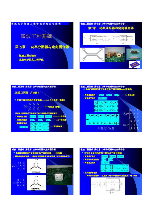
微波工程基础 第七章 功率分配器和定向耦合器 理想定向耦合器的散射参数
微波工程基础 第七章 功率分配器和定向耦合器 各端口都匹配的无耗非互易三端口网络——环形器
网络是匹配的 网络是无耗的
2
三端口网络(T型结)
任意三端口网络的散射参数——9x2个自由度(参数)
S11 S S 21 S31 S12 S 22 S32 S13 S 23 ——9x2个自由度(参数) S33
Wilkinson等分功率分配器,奇偶模分析法
S12 (S13)
e 偶模 V1 jV0 2
求Z,r
S11=0 可算出 Z 2 Z 0
V2e V0
S22 0
S12 (S13)
r 2 ?:保证奇模S22为0
奇偶模分析法 思想?
要点:1、偶+奇=单端口分析 2、所有端口加匹配负载 2、支路串联结构
S13 S 31 S 22 0
2 2 2
S11 0
S 22 0
S 33 0
——6x2个自由度
四.功分器和定向耦合器的设计

C10logP P1320logS31
dB[S(3,1)]
• 隔离度: 隔离端口4的输出功率P4和输入端口1的输入功率P1之比:
I10logP P1 420logS41 dB[S(4,1)]
定向耦合器的基本原理
• 8-16GHz倍频程内定向度: S41/S31<-17dB
• 8-16GHz倍频程内隔离度: S41<-20dB
定向耦合器的仿真设计
建立耦合器设计的电路原理图
耦合端口
输入端口
直通端口
隔离端口
/4;f012GHz
定向耦合器的仿真设计
建立耦合器设计的电路原理图
耦合端口
输入端口
直通端口
功分器的设计、仿真、优化
设置完成的功分器电路图
功分器的设计、仿真、优化
开始仿真 全频段内隔离度未达指标,并且平坦度较差,需优化
功分器的设计、仿真、优化
电路优化
• 对阻抗匹配电路的优化---优化变量w2,lh
功分器的设计、仿真、优化
电路优化
• 优化仿真器和优化目标的设置—由于电路对称性,S(3,1)和S(3,3)不需优化
dB[S(2,1)]
C1310logP P 3 i 20logS13
dB[S(3,1)]
功分器的基本原理
功分器的基本指标
• 输出端口间的隔离度: 根据输出端口2的输出功率P2与输出端口3的输出功率P3之比计算
• 功分比:
C2310logP P2 320logS S1 12 3
• 定向耦合器属于无源微波器件,为四端口器件,分为:
隔离
耦合
实验三功分器的设计制作与调试
36
功分器电路的调试(续)
需要测试的参数主要有以下几个
S11,S22,S33:输入,输出端口的反射系数 S21,S31:正向传输系数,要测幅度及相位 S23,S32:两输出端口的间隔离度
根据S21,S31的幅度和相位可以得到两个 输出端口的功分比以及相位平衡度.
37
功分器电路的调试(续)
观察网络分析仪测量的结果是否达到指 标要求并与前面仿真的结果做比较. 把实际测量的电路尺寸置于ADS软件中 进行仿真,把结果与实际测量结果相比 较. 如果测试结果与设计要求相差过多,则 需对电路进行调整,直至重新进行设计, 制版.
22
观察仿真曲线
优化完成后必须关掉优化控件,才能观察仿真的曲线.方 法是点击原理图工具栏中的 按钮,然后点击优化控件 OPTIM,则控件上打了红叉表示已经被关掉. 要想使控件重新开启,只需点击工具栏中的 按钮,然 后点击要开启的控件,则控件上的红叉消失,功能也重新 恢复了. 对于原理图上其他的部件,如果想使其关 闭或开启,也可以采取同样的方法. 点击工具栏中的Simulate 按钮进行仿真, 仿真结束后会出现图形显示窗口.
10
生成功分器的原理图
在原理图设计窗口中选择微带电路的工具 栏 窗口左侧的工具栏变为右图所示 选择微带线 以及 控件MSUB 分别放置在绘图区中 选择画线工具 将电路连接好, 连接方式见下页图(本图只是提 供参考,还有其它形式可供选择.)
11
功分器的原理图示例
12
设置微带电路的基本参数
双击图上的控件MSUB设置微带线参数
14
设置微带器件的参数
双击每个微带线设置参数,W,L分别设为相 应的变量或常量,单位mm,注意上下两臂的 对称性.
15
功分器设计原理

功分器设计原理嘿,朋友们!今天咱来聊聊功分器设计原理这档子事儿。
你说这功分器啊,就好比是一个神奇的分配大师。
想象一下,有一股力量,就像水流一样,要被均匀地分到不同的地方去,这就是功分器要干的活儿。
它是咋做到的呢?其实啊,就跟咱分东西一样。
比如说有一堆糖果,要分给几个小朋友,得保证每个小朋友都能拿到差不多的糖果数量,不能这个多那个少,对吧?功分器也是这样,要把输入的信号能量,合理地分配到各个输出端口。
这其中的关键就在于它的内部结构啦。
它就像是一个精心设计的迷宫,信号在里面走来走去,最后就被准确地分开啦。
这里面的线路啊、元件啊,都得搭配得恰到好处,就像拼图一样,缺了一块儿都不行。
而且哦,这功分器还得很稳定可靠呢!不能今天分好啦,明天就出岔子。
就好比你给小朋友分糖果,今天分对了,明天就乱分一气,那怎么行呢?所以啊,在设计的时候就得考虑各种因素,什么温度啦、湿度啦,都不能影响它的正常工作。
你说要是功分器设计得不好会咋样?哎呀,那可就麻烦啦!信号可能就不能准确地到达该去的地方,就像送快递送错了地址一样,那后果可不堪设想啊!再说说这功分器的种类吧,那也是五花八门的。
有等分的,有不等分的,就像分糖果,有的是平均分,有的是按需分配。
每种都有它自己的用处和特点,得根据实际情况来选择。
咱平时生活里不是也经常会遇到要分配东西的情况吗?这和功分器的原理其实差不多呢!只不过功分器是在信号的世界里工作罢了。
总之啊,功分器设计原理可真是个有意思的东西,它虽然看不见摸不着,但却在各种电子设备里默默地发挥着重要作用呢!没有它,好多设备可就没法正常工作啦。
所以啊,可别小看了这个小小的功分器,它可是电子世界里的大功臣呢!原创不易,请尊重原创,谢谢!。
功分器的设计与仿真

U D C:D10621-408-(2015)0544-0 编 号:2011022006
成 都 信 息 工 程 大 学 学 位 论 文
宽带 Wilkinson 功分器的设计
论文作者姓名: 申请学位专业: 申请学位类别: 指导教师姓名 (职称) : 论文提交日期:
叶建梅 电子信息科学与技术 工学学士 夏运强 2015 年 5 月 22 日
关键词:宽带, Wilkinson 功分器, 奇偶模,仿真
I
The Design of the Broadband Wilkinson Power Dividers
ABSTRACT
Power divider divide one power into two or multiple branches .Traditional Wilkinson power divider bandwidth is very narrow,and often can not meet the application broadband systems.In order to improve the above problems, the article describe wideband power divider’s design. This article aims to research and analysis related components and working principle of power dividers. It describes the use of odd-mode analysis method of a Wilkinson N-way power divider .This Wilkinson power divider’s design have a wideband of 0.8 ~ 2.5GHz.The power divider requires its insertion loss less than 1dB, isolation greater than 20dB and the voltage standing wave ratio (VSWR) less than 1.5.It focuses on the power divider’s design parameters calculation and optimization process.Then using ADS software principle and HFSS simulation of electromagnetic obtained debugging parameters , finally made the PCB in CAD and processed into a kind. In terms of software simulation results under ideal conditions on the test results or physical design diagram show the power divider met the target requirements.Since the required operating frequency is within ISM band, it can be used for wireless LAN, Bluetooth, ZigBee and other wireless networks.
- 1、下载文档前请自行甄别文档内容的完整性,平台不提供额外的编辑、内容补充、找答案等附加服务。
- 2、"仅部分预览"的文档,不可在线预览部分如存在完整性等问题,可反馈申请退款(可完整预览的文档不适用该条件!)。
- 3、如文档侵犯您的权益,请联系客服反馈,我们会尽快为您处理(人工客服工作时间:9:00-18:30)。
42High Frequency ElectronicsHigh Frequency DesignCOMBINERS & COUPLERSFrom February 2008 High Frequency Electronics Copyright © 2008 Summit Technical Media,LLC44High Frequency ElectronicsFigure 35 · Equivalent circuits of lumped LC-type 46High Frequency Electronics48High Frequency Electronics50High Frequency ElectronicsFebruary 200851High Frequency Design COMBINERS & COUPLERSof the high-pass section shown in Fig.39(b) could reso-nant with the shunt capacitors of the low-pass section at the center bandwidth frequency,in order to completely remove these components.Figure 39(c) shows the circuit diagram of the reduced-size ring hybrid with the charac-teristic impedances of the transmission-line sections of 100 Ωand their electrical lengths of 45 degree [61].As a result,the overall reduced hybrid size is more than 80 percent smaller than that of the conventional hybrid.This article series will conclude next month.The final topic is coupled-line directional couplers.References53.S.B.Cohn and R.Levy,“History of Microwave Passive Components with Particular Attention to Directional Couplers,”IEEE Trans.Microwave Theory Tech.,vol.MTT-32,pp.1046-1054,Sept.1984.54.J.Reed and G.J.Wheeler,“A Method of Analysis of Symmetrical Four-Port Networks,”IRE Trans.Micro-wave Theory Tech.,vol.MTT-4,pp.246-252,Oct.1956.55.R.Levy and L.Lind,“Synthesis of Symmetrical Branch-Guide Directional Couplers,”IEEE Trans. Microwave Theory Tech.,vol.MTT-16,pp.80-89,Feb. 1968.56. A.Grebennikov,RF and Microwave Power Amplifier Design,New York:McGraw-Hill,2004.57.P.Meaney,“A Novel Branch-Line Coupler Design for Millimeter-Wave Applications,”1990 IEEE MTT-S Int. Microwave Symp.Dig.,pp.585-588.58.L.F.Lind,“Synthesis of Asymmetrical Branch-Guide Directional Coupler-I mpedance Transformers,”IEEE Trans.Microwave Theory Tech.,vol.MTT-17,pp.45-48,Jan.1969.59.R.K.Gupta,S.E.Anderson,and W.J.Getsinger,“mpedance-Transforming 3-dB 90° Hybrids,”IEEE Trans.Microwave Theory Tech.,vol.MTT-35,pp.1303-1307,Dec.1987.60.S.Kumar, C.Tannous,and T.Danshin,“A Multisection Broadband I mpedance Transforming Branch-Line Hybrid,”IEEE Trans.Microwave Theory Tech.,vol.MTT-43,pp.2517-2523,Nov.1995.61.T.Hirota, A.Minakawa,and M.Muraguchi,“Reduced-Size Branch-Line and Rat-Race Hybrid for Uniplanar MMI C's,”IEEE Trans.Microwave Theory Tech.,vol.MTT-38,pp.270-275,March 1990.62.M.Caulton,B.Hershenov,S.P.Knight,and R.E. DeBrecht,“Status of Lumped Elements in Microwave I ntegrated Circuits - Present and Future,”IEEE Trans. Microwave Theory Tech.,vol.MTT-19,pp.588-599,July 1971.63.R.W.Vogel,“Analysis and Design of Lumped- and Lumped-Distributed-Element Directional Couplers for MI C and MMI C Applications,”IEEE Trans.Microwave Theory Tech.,vol.MTT-40,pp.253-262,Feb.1992.64.S.J.Parisi,“180° Lumped Element Hybrid,”1989 IEEE MTT-S Int.Microwave Symp.Dig.,pp.1243-1246.65.R.C.Frye,S.Kapur and R.C.Melville,“A 2-GHz Quadrature Hybrid I mplemented in CMOS Technology,”IEEE J.Solid-State Circuits,vol.SC-38,pp.550-555, March 2003.66. F.Ali and A.Podell,“A Wide-Band GaAs Monolithic Spiral Quadrature Hybrid and its Circuit Applications,”IEEE J.Solid-State Circuits,vol.SC-26,pp. 1394-1398,Oct.1991.67.W.A.Tyrrell,“Hybrid Circuits for Microwaves,”Proc.IRE,vol.35,pp.1294-1306,Nov.1947.68. C.Y.Pon,“Hybrid-Ring Directional Coupler for Arbitrary Power Divisions,”IRE Trans.Microwave Theory Tech.,vol.MTT-9,pp.529-535,Nov.1961.69.S.March,“A Wideband Stripline Hybrid Ring,”IEEE Trans.Microwave Theory Tech.,vol.MTT-16,pp. 361,June 1968.70.G.L.Matthaei,E.M.T.Jones,and L.Young, Microwave Filters,Imped ance-Matching Networks and Coupling Structures,New York:Artech House,1980.71. C.-H.Ho,L.Fan,and K.Chang,“Broad-Band Uniplanar Hybrid-Ring and Branch-Line Couplers,”IEEE Trans.Microwave Theory Tech.,vol.MTT-41,pp. 2116-2124,Dec.1993.72.T.Wang and K.Wu,“Size-Reduction and band-Broadening Design Technique of Uniplanar Hybrid Ring Coupler Using Phase I nverter for M(H)MI C’s,”IEEE Trans.Microwave Theory Tech.,vol.MTT-42,pp.198-206, Feb.1999.73. D.I.Kim and Y.Naito,“Broad-Band Design of Improved Hybrid-Ring 3-dB Directional Couplers,”IEEE Trans.Microwave Theory Tech.,vol.MTT-30,pp.2040-2046,Nov.1982.Author InformationAndrei Grebennikov received his Dipl.Ing.degree in radio electronics from Moscow I nstitute of Physics and Technology and PhD degree in radio engineering from Moscow Technical University of Communications and Informatics in 1980 and 1991,respectively.He has exten-sive academic and industrial experience working with Moscow Technical University of Communications and I nformatics,Russia,I nstitute of Microelectronics, Singapore,M/A-COM,Ireland,and Infineon Technologies, Germany and Austria,as an engineer,researcher,lectur-er,and educator.He read lectures as a Guest Professor in University of Linz,Austria,and presented short courses and tutorials as an I nvited Speaker at I nternational Microwave Symposium,European and Asia-Pacific Microwave Conferences,and Motorola Design Centre, Malaysia.He is an author of more than 70 papers,3 books and several European and US patents.He can be reached by grandrei@.52High Frequency Electronics。