三路威尔金森功分器设计 3 way wilkinson
微波工程威尔金森功率分配器

仿真结果
输入端口、输出端口的回波损耗在 三个频带内都优于13dB。
04
结论
慢波结构通过减小相位速度从而减小了 增加了电尺寸从而减小了电路尺寸;基 于QWOS的滤波器获得了三个工作频带。 通过使三个滤波器根据所需频率放置在 经过精确计算的50欧姆传输线上的不同 位置,来准确获得了三个通频带,同时 具有低插入损耗。与其他现有研究相比 较,除了有轻微的电路面积增加以外, 具有了40%、10.5%、17.9%的更宽的 相对带宽。
• 一个宽频带的和一个新型的基于QW OS的三频带带通滤波器
威尔金森功率分配器
由威尔金森1提出的匹配的对称双功率分 频器,是用于相同的幅值/相位功率划分 的拓扑结构之一。威尔金森提出了匹配的 双向功率分配器的基本配置,即 三个特性阻抗需满足关系1:1.414:2:1 ,同时在两个输出端口之间引入一个电阻, 从而增强了它们之间的隔离。由于威尔金 森的分频器利用一个四分之一波长的变压 器来将分割线与输入端口相匹配,变压器 的尺寸——特别是低频应用—— 的尺寸是无法接受的。使用传统的方法将 这种分频器的操作扩展到双/三波段,单/ 双阻抗变压器需要。因此,双/三带的功率 分器占据了更多的空间,增加了电路/芯片 的面积,特别是在使用低介电常数基板的
设计结果
经计算以及调试后的电路尺寸如图 所示,该设计达到了良好的性能, 获得了宽频带和低回波损耗的性能。
如左图所示,可以看出,在1.5、1.9、 2.35GHZ的三个中心频率上均有宽频 带,低损耗,插入损耗分别为0.009、 0.25、0.38db。
03
仿真结果
如图所示: 在1.5/1.9。2.35GHZ的三个频点上分别都 能实现接受到的功率为一端口输入功率的一 半,即S21=3db,且每个工作频率都有较 大带宽。在两个输出端口之间有大于15dB 的隔离度。
威尔金森是怎么设计出威尔金森功分器的?

威尔金森是怎么设计出威尔金森功分器的?威尔金森功分器是个好东西,在射频领域里面应用很广泛。
第一次认识它是在教科书上,书上介绍了他的原理,自己也琢磨了很久,也理解了奇偶模分析的方法和隔离电阻的作用。
但是一直想知道威尔金森是怎么设计出来的?我们是否也可以按照一定的思路设计功分器呢?下面就去找这个思路,最终找到的这个思路可以方便的设计各种各样的功分器,俺的同事已经实践了哈,大家看完也可以试验一把。
首先明确一下这个功分器的要求:1.在微波射频领域,能量是非常宝贵的,所以设计的功分器不能够额外损失能量,如果分为两路的话就是每一路损耗3dB,即︱S21︱=︱S31︱=0.7072.各端口均50欧姆匹配,且两个输出口的完全隔离,即︱S11︱=︱S22︱=︱S33︱=︱S32︱=︱S23︱= 0图2根据以上的要求,我们设计一个对称的功分器,这样就可以只考虑一个端口,上面条件的一半就可以了,即︱S21︱=0.707,︱S11︱=︱S22︱=︱S32︱=0。
如图2所示,从中间把这个我们要设计的功分器分开,两边的的电压都是一模一样的,处处都是开路点。
1.由于端口1匹配,所以输入阻抗为50欧姆。
从1端口输入的能量分为对称的两路,那么每一路的阻抗都是100欧姆。
这个功分器第一个任务的就要用开路线左边的部分把端口2的50欧姆变换到100欧姆,且无损耗。
2.根据微波网络的理论,如果我们使用的都是电容,电感,传输线,电阻这些互易原件,那么整个功分器也就是互易的(关于对这个理论的理解后面文章会给出解释)。
即︱S2 1︱=︱S12︱=0.707。
也就是从端口2到端口1的能量为一半,那另外一半呢?又不能反射回去,又不能泄漏到端口3。
所以这个功分器的第二个任务就是要有一个电阻来吸收端口2入射过来的一半能量。
这个需求太抽象了,还要细化分解,下面利用奇偶模的方法来分析一下。
如下图所示,从端口2输入一个电压幅度为1的波,分解为奇偶模式,偶模式就是1端口输入情况下功率分配的逆过程,端口2、3均无反射波,有一半的能量从端口1输出,那么奇模的能量必须都要消耗到电阻上,不能有反射波回来。
新型三等分Wilkinson功分器在高效率功放中的应用

第 5卷 第 8 1 期
2 1 年 8月 01
电讯技术
T lc mmu iain E gn e i e o e n c t n i e r g o n
V 15 N . 0. 1 o8
Au g.2 1 01
文章 编号 :0 1 9X(0 10 03 —0 10 —83 21 l8— 18 5
t e n w o rdvd ri 9 mm 1 mm,i 1 h e p ,t e is rin ls sls a 4 d 1 h n et o si e st n 0. B,te i - o h h s o
新 型三等 分 Wi i o l n n功分器在 高效率功放中的应用 ks
陈 慰 陶学敏2赵 娜 , ,
(. 天恒 星空间技 术应 用有限公司 , 1航 西安 707 ;. 1 72重庆大学 通信工程学院 , 0 重庆 403) 000
摘 要: 针对一种新型的三路 D h啊 功率放 大器, oe 为满足其对称结构要求 , 在传统对称结构二等分 功分 器基 础上 , 结合 三路 D hr 功放 电路 尺 寸 , oey t 通过 理论 计 算和采 用 A S软件 仿 真的 方法设 计 了对 D
前提 下 , 功分 器性 能指 标满足 功放 电路 三路 相位 一致 性设计 要 求 , 高 了放 大器工作 效 率 , 试 结果 提 测 显 示饱 和点 工作效 率 高 于两路 D h r oet 率放 大器 。 y功
基于多层PCB的三路威尔金森功分器设计
Ab s t r a c t : Pr o p o s e d a no v e l 3 -wa y W i l k i ns o n d i v i d e r ba s e d o n mu l ihy t e r PCB t e c h n i q u e s . A 3-wa y d i vi d e r i s a l s o d e s i g ne d a s a n i n s t a n c e . Bo t h c i r c ui t a n d e l e c t r o ma ne g i t c s i mu l a io t ns a r e e mp l o ye d f o r a n a l yz e a nd v e r i ic f a t i o n . wh i l e g oo d a g r e e me n t i s o b t a i ne d- Ke y Wo r ds : mul il t a y e r PCB e mb e d d e d r e s i s t o r W i l k i n s o n d i v i d e r 3 -w a y
得 到 了较 为理想 的性 能, 并 与理论 值得 到 了较好 的 吻合 。 关键词 : 多层 印制板 内埋 电阻 威 尔金 森功 分器 3 路 中图分 类号 : T N 4 0 5 文献 标识码 : A
文章编 号: 1 0 0 7 — 9 4 1 6 ( 2 0 1 4 ) 0 3 - 0 1 4 8 - 0 2
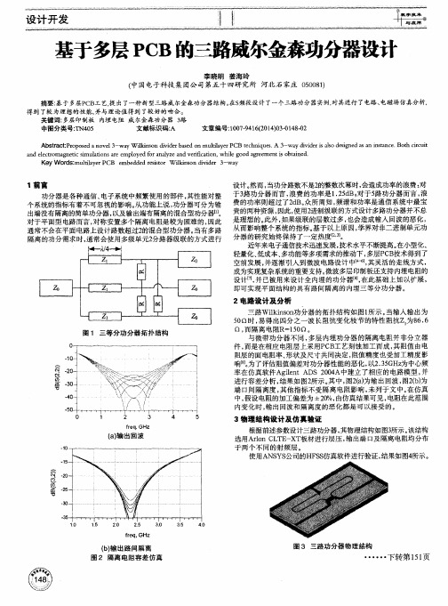
设计 。 然而 , 当功分路数不是2 的整数次幂时, 会造成功率的浪费: 对 于3 路功分器而言 , 浪费的功率是 1 . 2 5 d B, 对于5 路功分器而言 , 浪 费 的功率 则超过了2 d B。 众所周知, 频谱和功率是通信系统 中最宝 贵的两种资源 , 因此 , 使用2 进制级联 的方式设计多路功分器并不总 是理想 的。 此外 , 如果级联 的层数过多 , 也会造成输入回波的恶化 , 从而影响整个系统 的指标 。 基于 以上原 因, 学界对非二进 制单元功 分器的研究始终保持 了一定 热度【 2 . ] 1 。 近年来 电子通信技术迅速发展 , 技术水平不断提高。 在小型化 、 轻量化、 低成本 、 多功能等多项需求的推动下 , 多层P C B 技术得到了 空前发展 , 并逐渐引入到微波 电路设计 中 l , 其灵活的走线方式 , 成为实现复杂系统 的重要支持 。 微波多层 印制板还支持 内埋 电阻的 设计[ 7 】 , 并 已被 用 来 设 计 全 内埋 的功 分 器 【 8 1 , 在 此 基 础 上 加 以扩 展 , 即可实现平面结构 的具有路 间隔离的内埋三等分功分器 。
威尔金森功分器设计-毕业论文

摘要摘要功率分配器简称功分器,在被用于功率分配时,一路输入信号被分成两路或多路较小的功率信号。
功率合成器与功率分配器属于互易结构,利用功率分配器与功率合成器可以进行功率合成。
功分器在相控阵雷达,大功率器件等微波射频电路中有着广泛的应用。
现在射频和微波系统的设计越来越复杂,对电路的指标要求也越来越高,电路的功能也越来越多,电路的尺寸越来越小,而设计周期越来越短,传统的设计方案已经不能满足微波电路设计的需求,使用微波软件工具进行微波系统的设计已经成为微波电路设计的必然趋势。
小型低功耗器件是射频电路设计的研究热点,而微带技术具有小型化低功耗的优点,为此我学习了功分器的基本原理,结合当下的实际情况,设计了一个Wilkinson功分器,并使用基于矩量法的ADS软件设计、仿真和优化计算相关数据参数,进行参数的优化,并制作了一个性能良好的Wilkinson功分器。
关键词:功分器,ADS,优化参数IABSTRACTABSTRACTPower divider is referred to as power divider,in which the input signal is divided into two(or more)smaller power signals when the power distribution is used.Power synthesizer,and a power divider is reciprocity structure,power synthesis can be carried out using the power splitter and combiner.Power divider is widely used in phased array radar,high power devices and other microwave circuits.Now the design of RF and microwave system is more and more complex,the circuit requirements are also getting higher and higher,more and more functions of the circuit,the circuit size is getting smaller and smaller and design cycle becoming shorter and shorter,the traditional design scheme has been unable to meet the demand of microwave circuit design,using microwave software tools for the design of microwave system has become the inevitable trend of the microwave circuit design.small size and low power consumption devices is the focus of the research on the RF circuit design,and microstrip technology has the advantages of miniaturization and low power consumption.Therefore,I learned the basic principle of power divider,combined with the current actual situation,the design of the a Wilkinson power divider,and use based on method of moments of the ADS software to design,simulation and optimization calculation parameters,parameter optimization,and produced a good performance of Wilkinson power divider.Key words:power divider,ADS,optimization parametersII目录第1章引言 (1)1.1功分器的发展概况 (1)第2章研究理论基础 (2)2.1功分器的理论基础 (2)2.2功分器技术基础 (4)2.2.1什么是功分器 (4)2.2.2功分器的重要性 (4)2.2.3Wilkinson功分器的优点 (4)2.3wilkinson基本工作原理: (5)2.4Wilkinson功率功分器的基本指标 (6)2.4.1.输入端口的回波损耗 (6)2.4.2插入损耗 (7)2.4.3输入端口间的隔离度 (7)2.4.4功分比 (7)2.4.5相位平衡度 (7)第3章ADS的介绍 (8)3.1ADS趋势 (8)3.2线性分析 (9)3.3电磁反正分析 (10)3.4仿真向导 (10)第4章功分器的原理图设计仿真与优化 (12)4.1等分威尔金森功分器的设计指标 (12)4.2建立工程与设计原理图 (12)4.2.1建立工程 (12)4.2.2设计原理图: (13)4.2.3基板参数设置 (16)4.2.4基板参数输入 (18)4.2.5插入VAR (19)4.2.6VAR参数设置 (19)4.2.7VAR微带线 (19)4.3功分器原理图优化仿真 (21)4.4功分器优化版图生成 (24)4.5功分器优化 (24)4.6功分器的版图生成与仿真 (31)第5章结论 (36)参考文献 (37)致谢 (38)外文资料原文 (39)译文 (41)第1章引言第1章引言1.1功分器的发展概况功率分配器是将输入信号功率分成相等或不相等的几路输出的一种多端口的微波网络,广泛应用于雷达,多路中继通信机等大功率器件等微波射频电路中。
威尔金森是怎么设计出威尔金森功分器的

威尔金森是怎么设计出威尔金森功分器的威尔金森功分器是一种用于将输入信号分解为功率成分的电路。
它由英国工程师威尔金森于1947年设计,并在1950年的《电子工程师杂志》上发表。
这个电路设计的初衷是为了解决实际电路中功率测量的问题。
威尔金森功分器的设计是基于一种被称为“复制器”的元件。
复制器是一种有两个输入端和两个输出端的电路,其特点是在两个输出端上复制输入信号。
复制器的设计实现了信号的复制,这在威尔金森功分器的设计中起到了关键作用。
威尔金森功分器的电路结构如下:是一种常用的微波功分器,广泛应用于无线通信和雷达系统中。
它能将输入信号均匀地分配到两个输出端口,并且具有较宽的工作频率范围和较低的插入损耗。
本文将介绍威尔金森功分器的设计原理和仿真方法。
1.威尔金森功分器的设计原理```┌─Z1─┐RF in ─┤ ├─ Z2 ─ RF out1├─Z0─┤└─Z3─┘RF out2```其中,RF in为输入端口,RF out1和RF out2为输出端口,Z0为特征阻抗,Z1和Z2为等效阻抗,Z3为耦合阻抗。
在设计过程中,首先需要确定特征阻抗Z0的数值,一般为50欧姆。
然后,根据所需的功分比例,计算等效阻抗Z1和Z2的数值。
最后,选择合适的耦合阻抗Z3,使得整个电路达到最佳的工作性能。
2.威尔金森功分器的仿真方法首先,打开ADS软件并创建一个新的工程。
然后,在工程中添加一个新的设计,选择“Schematic”类型。
在Schematic设计界面中,依次添加所需的元件,包括传输线、阻抗匹配器和耦合器。
其中,传输线用于连接输入端口和输出端口,阻抗匹配器用于实现输入和输出的阻抗匹配,耦合器用于实现信号的均匀分配。
接下来,设置传输线的特性阻抗和长度,以及阻抗匹配器和耦合器的阻抗数值。
通过调整这些参数,可以实现所需的功分比例和工作频率范围。
完成电路设计后,可以进行仿真和优化。
选择“Simulation”菜单,设置仿真参数,如频率范围和步长。
然后,运行仿真并得到结果。
根据仿真结果,可以评估电路的性能,并进行优化。
如果需要改变功分比例或工作频率范围,可以调整各个元件的数值,并重新运行仿真。
最后,完成电路设计和优化后,可以进行PCB布局和封装设计。
根据实际需求,选择合适的材料和尺寸,并进行布局和封装设计。
总结:本文介绍了威尔金森功分器的设计原理和仿真方法。
通过合理选择和调整各个元件的数值,可以实现所需的功分比例和工作频率范围。
威尔金森功分器总结
Z 03 Z 0 (1 K 2 ) K 3 ;
R
(1 K 2 ) Z0 ” K
2. 威尔金森功分器技术指标 频率范围,中心频率 f0 和带宽 BW 频带内输入端口的回波损耗,C11 频带内的插入损耗,C21,C31 两个输出端口之间的隔离度,C23 二、正文 功分器的技术指标主要包括频率范围、端口电压驻波比或回波损耗、输入输出间的传输损耗、输出端 口间的隔离度。 1. ADS 仿真威尔金森功分器 1.1 技术指标如下图所示:
图2
ADS 仿真时的技术指标
1.2 仿真流程: 1.2.1 创建项目和原理图
1.2.2 原理图建模 1)将 MUSB 插入原理图画图区,在画图去双击 MUSB,弹出设置对话框,对微带线设置参数设 置如下:
2 )在菜单中选择变量 VAR 空间,插入到原理图的画图区,双击空间 VAR ,分别设置四个变量 W50,W70,L1,L2,L3,L4,Lx,分别赋值为 8.2,4.6,11,12,4,13,5。这里取这些值的依据在于下 图所示:
3)
4)
5)画出原理图如下:
6) 原理图的仿真:通过添加 S 参数求解器 SP。对 SP 的设置如下所示:
计算结果如下图:
7) 生成版图: 注:在生成版图前需要关闭与生成版图无关的项目,否则生成会出现各种各样的 bug。 同时,生成版图可以帮助我们很快地检查出那些语法上的错误,如单位错误
这里:L = L1+L2+(W50)/2
图 1 理想 3dB 微带 Wilkinson 功分器示意图 端口 1 输入,端口 2 和 3 作为输出。中间粉色的为隔离电阻。 由于结构对称,各路信号经过的电长度相同,因此在输出端口处于相同的电位,此时隔离电阻不消耗 任何功率。假如信号由于某种原因在输出端口 2 处发生反射,则反射信号功率一部分经过隔离电阻 R 传至 输出端口 3,另一部分功率反射回输入端口,并在支线处再度分配,重新由两支路传输至两个输出端口。由 于阻抗变换线的长度为λ/4,则两路反射信号到达端口 3 时的电长度相差 180 度,所以在端口 3 处,两路信 号幅度相等、相位 相反,彼此相消,从而实现两输出端口之间的相互隔离。对于任意分配比的混合型功率 分配器,隔离电阻的作用相同。 隔离电阻的作用: “从隔离电阻那里开始走起,左右对称,每边都是 1/4 波长,信号走完这两个 1/4 波长 后到达隔离电阻的另一端,但这个时候,在隔离电阻两端信号的电压正好相反,一起走了 1/2 个波长,可以在隔 离电阻上消耗,这样到达另一个端口的信号就没什么了,起到了隔离的作用.”
威尔金森(wilkinson)功分器设计
此功分器比较简单。
如果只是做仿真,ADS较为方便,如果要做实物或产品的话,HFSS比较可靠。
本人亲测HFSS仿真结果和实物基本一致,ADS差别不一。
多节功分器原理和单节一样,网上有多节等分功分器归一化数据表格,按照表格中的值球的传输线阻抗得到的功分器只需要少许优化即可。
接下来以双节8-11G功分器大致介绍一下设计流程。
如图所示,L0和L3都是Z0阻抗的传输线,一般选择为50Ω,在ADS中可以算出现款和线长,线的长度L0和L3对功分器没太大影响,所以在做的时候可以根据要求增加或减少。
因为是8-11G的,f2/f1<1.5,所以双节的都满足要求,可以用频带宽度比为1.5的功分器,这样的话隔离度更好。
查表得到L1L2归一化阻抗分别是1.1998和1.6070归一化电阻为5.3163和1.8643,得到阻抗和电阻值分别是60、80.33和93、265,注意的是电阻顺序是倒过来的这样分别用微带线计算软件算得两段线的带宽和π/4线长,分别是0.324/6.28和0.653/6.15,这样在HFSS中九可以建立模型仿真,在建模的时候做成参数模型,这样可以调节和优化,电阻直接在合适的地方画一个矩形,右键lumped RLC可以设置。
模型可以做成实际的0.035mm的铜,也可以设置成perfect E,大致都差不多,我做过一个,实测和仿真基本上一致,损耗都在3.2左右,隔离倒是有点差,差了约5db。
有些做成弧形,原理都是一样,个人觉得倒是美观很多。
弧形这个是我对上面功分器改变形状得来的,出来的效果只是差了一点点。
对了,基片背面需要铺地,否则仿真时可能有问题,本人也是兴趣自己做着玩的,不是专业的,有错请指正,有需要模型或交流的可以联系我,最后总结一下。
1、建模的时候最好建立参数模型,可调可优化;2、基板背面最好铺地;3、在仿真的时候波端口向量应该向接地(向下);4、归一化电阻值顺序和归一化阻抗是相反的;5、输入端的驻波比要好好仿真,容易变差;。
大连海事大学射频电路设计威尔金森功分器设计实验报告
实验二:wilkinson 功分器设计报告一、实验目标1. 掌握功分器的原理及基本设计方法。
2. 学会使用电磁仿真软件ADS 对功分器进行仿真。
3. 掌握功分器的实际制作和测试方法,提高动手设计能力。
二、实验要求1. 充分做好实验前的准备工作,认真学习电磁仿真软件ADS 。
2. 掌握微波器件和微波测试仪器的使用方法,以免损坏器件和仪器。
3. 分析仿真结果与测试结果,记录必要数据。
三、设计思路四、理论设计:Wilkinson 功率分配器有三端口网络构成,如下图,信号由端口1输入,端口2和端口3输出。
理想3dB 微带wilkinson 功率分配器的散射参量为 S=-1/因为S11=S22=S33=0,所以理想状态下在中心频率,三个端口是完全匹配的。
因为S21=S31=-j/ ,所以在端口1有输入而其他端口匹配时,端口2和端口3有等幅同相的输出,并且都比输入信号之后90度,这说明这是一个功分比为1的3dB 功率分配器。
因为S23=S32=0,所以这个功率分配器两个支路是完全隔离的。
因为有 段,所以这个功率分配器不是带宽器件。
功分器的技术指标主要包括频率范围、端口电压驻波比或回波损耗、输入输出间的传输损耗、输出端口间的隔离度。
1.频率范围频率范围是各种射频和微波电路工作的前提,功率分配器的设计结构和尺寸大小与工作频率有密切关系,必须首先明确功分器的工作频率,才能进行具体的设计工作。
本实验取,中心频率f0=1GHz 带宽BW :0.9GHz —1.1GHz 。
2.端口的电压驻波比(回波损耗)理论设计ADS 软件仿真加工制作实验测试调试修正端口的电压驻波比或反射系数是射频和微波电路的一个重要指标,它反映了端口的匹配状况。
端口1,端口2和端口3的电压驻波比或反射系数,分别有散射参量S11,S22,S33决定。
其中端口1的电压驻波比为用同样方法可以测得端口2和端口3的电压驻波比和回波损耗。
3.输入输出时间的传输损耗定义为输出端口2(端口3)的输出功率P2(P3)和输入端口1的输入功率P1之比,记为输入输出时间的传输损耗是由于传输线的介质或者导体不理想等原因导致的,介质的损耗角正切和导体的电导率是形成损耗的原因。
- 1、下载文档前请自行甄别文档内容的完整性,平台不提供额外的编辑、内容补充、找答案等附加服务。
- 2、"仅部分预览"的文档,不可在线预览部分如存在完整性等问题,可反馈申请退款(可完整预览的文档不适用该条件!)。
- 3、如文档侵犯您的权益,请联系客服反馈,我们会尽快为您处理(人工客服工作时间:9:00-18:30)。
Three-way planar WilkinsonsUpdated November 13, 2011 Click here to go to our main page on Wilkinson splittersClick here to go to our page on N-way splittersClick here to go to our page on the Kouzoujian splitter, a great alternative to the conventional N-way WilkinsonNew for June 2010! This page will provide a basic analysis of planar, three-way Wilkinson splitters in 50 ohm system impedance. This is splitter is imperfect, because it is missing an isolation resistor between the two outer ports, however, this is what makes it easy to lay out. We divided the analysis into three "types" which are described below, and ranked according to bandwidth potential. Type 1 splitterThe Type 1 splitter is the simplest network possible. The three arms each employ a single quarter-wave impedance transformer. If you were to impedance match port 1 at center frequency, the transformers would all be 86.6 ohms (transforms each 50 ohm leg to 150 ohms, and three 150 ohms in parallel is 50 ohms). Sorry about the crummy schematic, you'd think by now Agilent would provide a means for graphic capture beyond the usual copy-and-past into Powerpoint, then shrink image with PaintShop...The variables R1 and Z1 were allowed to optimize to provide the maximum "-15 dB bandwidth", in other words, it was required that reflection coefficients S11, S22 and S33 and isolation terms S23 and S24 were less than -15 dB. Note that by symmetry, it is not necessary to optimize (or monitor) S44, and S43.The choice of -15 dB as the goal is arbitrary. However, in the planar three-way Wilkinson, you can't expect perfect isolation of the split ports, and without perfect isolation, you won't get perfect return losses for S22, S33 and S44.The transmission line impedance values were restricted to no more than 100 ohms (in all three types), to make the circuit realizable in microstrip. It might be better to restrict to a lower value depending on what substrate is chosen, and yield considerations. The subject for another day!For Type 1, Z1 was found to be 91.4 ohms and R1 was 83.6 ohms, resulting in -15 dB bandwidth of 39%.Below is the transmission coefficient, showing the near-ideal value of 4.78 dB[-10*log(1/3)]. All three transmission coefficients are equal in this simplified analysis, in practice the outer branches will behave slightly differently from the center branch.Here are the return losses and isolation. Note that all parameters are somewhat compromised, as expected. This is the price that is paid for a planar design with only two isolation resistors.Type 2In Type 2 we added another transformer section, in this case a single transformer at the input, and component values were reoptimized for maximum -15 dB bandwidth.The optimized results are shown below. We didn't bother to plot the transmission coefficient, it is similar to that of Type 1. Here, Z1 was found to be 41.9 ohms, Z2 was 91.4 ohms, and R1 was 76.9 ohms, resulting in -15 dB bandwidth of 75%.Type 3In Type 3, the second transformer section was moved to the output ports, and component values were reoptimized for maximum -15 dB bandwidth.The optimized results are shown below. Here, Z1 was found to be 99.3 ohms, Z2 was 54.7 ohms, and R1 was 98.6 ohms, resulting in -15 dB bandwidth of 53%.In conclusion, Type 2 offers the best bandwidth of the three splitters we examined. Note that if you needed more bandwidth, you could add more sections and a second (or third) set of dump resistors. Planar dividers have been made that span 2-18 GHz in this fashion, and people have been happy to spend $1000 on them!A further exampleThis example is of a two-stage three-way Wilkinson with two sets of isolation resistors. It was EM-analyzed by some students from India. Bravo!Below is the linear schematic. We accidentally cropped out the microstrip parameters. The microstrip substrate has ER 4.4, and is 1.5 millimeters in height. We left the conductivity as a PEC (perfect electrical conductor).And below is the optimization goals and constraints we put on the network. Here we didn't demand 15 dB for the isolation and return losses. We asked for 20 dB, but didn't try to calculate the exact bandwidth that it was capable of, over 65% bandwidth.Here is the result after optimization (the final values are given in on the schematic). We put a constraint on Z2, it was not allowed to exceed 100 ohms (it is often difficult to realize very high impedances). The parameter that has the least 20-dB bandwidth is S33, which is the return loss of the center leg. Whoops, looks like we also constrained R2 to 150 ohms, there was no reason to put any constraints on the isolation resistors' values.What happens when you don't have any resistors in the network? In the schematic below the resistors have all been deactivated.The input match (S11) looks the same, while the output matches and isolations have been severely degraded. This is obvious if you study even and odd mode analysis.Here is the EMed layout of the divider. You can see how the tool divided the network into tiny triangles, upon which Maxwell's Equations are imposed. The resistors (drawn and multi-colored ovals) are not part of the EM analysis, so we don't expect much isolation. The Line lengths in the layout have been folded to achieve approximately 44 mm length to agree with the linear schematic. Why are their elbows in the upper and lower paths? The electrical length through an elbow is some non-zero value. By putting equal number of elbows in each path, you can compensate for them all at once by trimming the three legs' high impedance sections simultaneously. Note that in this layout there are three elbows in the upper and lower paths, and four in the center one, so we slightly violated our intentions...And here are some of the parameters, analyzed in an EM tool. Here's the reflection coefficient, which looks similar to the linear analysis but is a more accurate representation of what the circuit will do. Note that it has less return loss at the center of the band than we wanted. Welcome to the real world!And below are the three transmission coefficients, which are remarkable similar. Good job!A postulated ruleOne of the most basic rules of network theory is for a three-port circuit, you cannot have all ports simultaneously matched if it is lossless (no resistors). We're not going to step out on a limb and say that the same is always true for a four-port (it's not, one example of a matched lossless four-port is a rat-race). But for "related reasons" that we are to lazy to prove, let's postulate that an "N-port Wilkinson-like power divider without resistors" can never be impedance matched at the output ports.。