二极管1N4007规格书
MEMORY存储芯片1N4007中文规格书

Leads are Readily Solderable
• Lead and Mounting Surface Temperature for Soldering Purposes:
1N4001, 1N4002, 1N4003, 1N4004, 1N4005, 1N4006, 1N4007
10
1.0E−04
1.0E−05
TC = 150°C
1
TC = 100°C
1.0E−06
TC = 100°C
1.0E−07
TC = 150°C
0.1 0.5
TC = 25°C
0.6 0.7 0.8 0.9
THERMAL CHARACTERISTICS Rating
Maximum Thermal Resistance, Junction−to−Ambient
Symbol RqJA
Max Note 1
Unit °C/W
IF, FORWARD CURRENT (A) IR, REVERSE CURRENT (A)
†For information on tape and reel specifications, including part orientation and tape sizes, please refer to our Tape and Reel Packaging Specifications Brochure, BRD8011/D.
1N4001S 1N4007S硅整流管规格书
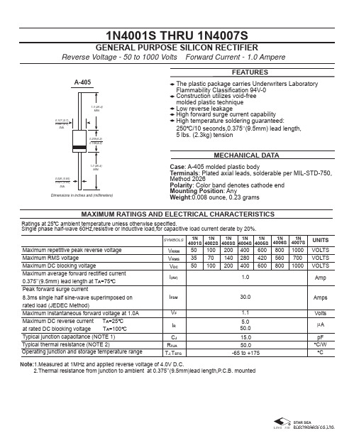
1N4001S THRU 1N4007SGENERAL PURPOSE SILICON RECTIFIERReverse Voltage - 50 to 1000 Volts Forward Current - 1.0 AmpereCase : A-405 molded plastic bodyTerminals : Plated axial leads, solderable per MIL-STD-750,Method 2026Polarity : Color band denotes cathode end Mounting Position : AnyWeight :0.008 ounce, 0.23 gramsThe plastic package carries Underwriters Laboratory Flammability Classification 94V-0Construction utilizes void-free molded plastic technique Low reverse leakageHigh forward surge current capability High temperature soldering guaranteed:250 C/10 seconds,0.375”(9.5mm) lead length,5 lbs. (2.3kg) tensionFEATURESMECHANICAL DATAMAXIMUM RATINGS AND ELECTRICAL CHARACTERISTICSA-405Dimensions in inches and (millimeters)50355010070100200140200400280400600420600800560800100070010001N4001S VOLTS VOLTS VOLTS SYMBOLSUNITS AmpAmps Volts V RRM V RMS V DC I (AV)I FSM V F 1.030.01.1Operating junction and storage temperature rangeMaximum repetitive peak reverse voltage Maximum RMS voltageMaximum DC blocking voltageMaximum average forward rectified current 0.375”(9.5mm) lead length at T A =75 C Peak forward surge current8.3ms single half sine-wave superimposed on rated load (JEDEC Method)Maximum instantaneous forward voltage at 1.0A Maximum DC reverse current T A =25 C at rated DC blocking voltage T A =100 C Typical junction capacitance (NOTE 1)Note:1.Measured at 1MHz and applied reverse voltage of 4.0V D.C.2.Thermal resistance from junction to ambient at 0.375”(9.5mm)lead length,P.C.B. mountedI R 5.050.0R θJA C J T J ,T STG50.015.0-65 to +175pF CA µTypical thermal resistance (NOTE 2)C/W 1N 4002S 1N 4004S 1N 4003S 1N 4005S 1N 4007S1N 4006S Ratings at 25 C ambient temperature unless otherwise specified.Single phase half-wave 60Hz,resistive or inductive load,for capacitive load current derate by 20%.RATINGS AND CHARACTERISTIC CURVES 1N4001S THRU 1N4007S0.6 0.8 1.0 1.2 1.4 1.50.01 0.1 1 10 1001001010.1REVERSE VOLTAGE,VOLTSt,PULSE DURATION,sec.FIG. 5-TYPICAL JUNCTION CAPACITANCEFIG. 6-TYPICAL TRANSIENT THERMAL IMPEDANCEFIG. 3-TYPICAL INSTANTANEOUS FORWARDCHARACTERISTICSNUMBER OF CYCLES AT 60 HzFIG. 2-MAXIMUM NON-REPETITIVE PEAK FORWARDFIG. 1- FORWARD CURRENT DERATING CURVEA V E R A G E F O R W A R D R E C T I F I E D C U R R E N T ,A M P E R E SI N S T A N T A N E O U S F O R W A R D C U R R E N T ,A M P E R E SJ U N C T I O N C A P A C I T A N C E ,p FP E A K F O R W A R D S U R G E C U R R E N T ,A M P E R E SINSTANTANEOUS FORWARD VOLTAGE,VOLTS1001010.10.01PERCENT OF PEAK REVERSE VOLTAGE,%FIG. 4-TYPICAL REVERSE CHARACTERISTICSI N S T A N T A N E O U S R E V E R S E C U R R E N T ,M I C R O A M P E R E ST R A N S I E N T T H E R M A L I M P E D A N C E ,C /WAMBIENT TEMPERATURE, C。
贴片二极管1N4007(M7)规格书
VDC
50 100 200 400 600 800 1000
IF(AV)
1.0
IFSM
30
IR(AV)
30
单位 Unit
V V V A A µA
典型热阻 Typical thermal resistance
RθJA
75
℃/W
工作结温和存储温度
Tj,ቤተ መጻሕፍቲ ባይዱTSTG
-50 --- +150
℃
Operating junction and storage temperature range
10
100
脉冲宽度 t, Pulse Duration, sec
-2-
IF = 1.0A
VF
1.1
V
Maximum forward voltage
最大反向电流 Maximum reverse current
TA= 25℃ TA=100℃
IR
5.0
µA
100
典型结电容 VR = 4.0V, f = 1MHz
Cj
15
pF
Type junction capacitance
-1-
反向电流 IR (mA) IR Instantaneous Reverse Current (mA)
峰值正向浪涌电流 IFSM(A) IFSM Peak Forward Surge Current (A)
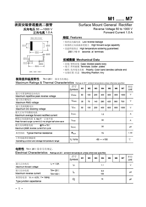
M1 ...... M7
浪涌特性曲线(最大值) MAXIMUM NON REPETITIVE PEAK FORWARD SURGE CURRENT
典型热阻 RθJA (℃/W) RθJA Transient Thermal Impedance (℃/W)
贴片二极管1N4007(M7)规格书
0.1
PULSE WIDTH=300ms 1%DUTY CYCLE
0.01
0.6
0.8
1.0
1.2
1.4 1.5
正向电压 VF(V) VF Instantaneous Forward Voltage (V)
典型结电容
TYPICAL JUNCTION CAPACITANCE
200
100
TJ=25°C
10
Resistive or
inductive Load
0.2
0
0
25
50 75 100 125 150 175
环境温度 Ta(°C) Tamb, ambient temperature (°C)
正向特性曲线(典型值)
TYPICAL FORWARD CHARACTERISTIC
20
10
Tj = 25°C
反向电流 IR (mA) IR Instantaneous Reverse Current (mA)
峰值正向浪涌电流 IFSM(A) IFSM Peak Forward Surge Current (A)
M1 ...... M7
浪涌特性曲线(最大值) MAXIMUM NON REPETITIVE PEAK FORWARD SURGE CURRENT
表面安装普通整流二极管
反向电压 50 ---1000 V 正向电流 1.0 A
SMA DO-214AC
.067(1.70) .051(1.29)
.110(2.79) .086(2.18)
.091(2.31) .067(1.70)
.059(1.50) .035(0.89)
.180(4.57) .160(4.06)
1N4007WS二极管

0.8
0.6
0.4
0.2
Single phase half-wave 60 Hz resistive or inductive load
0.0 25 50 75 100
125
150
175
Case Temperature (°C)
Instaneous Reverse Current (μA)
Fig.2 Typical Instaneous Reverse Characteristics
1N4001WS THRU 1N4007WS
SOD-323
1.40(0.055) 1.20(0.047)
2.75(0.108) 2.55(0.100)
1.80(0.07) 1.40(0.063)
.15(.0059) .08(.0031)
0.4(0.016) 0.25(0.0098)
1.10(.043) 0.80(.032)
MDD Catalog Number
SYMBOLS 4001
Marking code
Maximum repetitive peak reverse voltage Maximum RMS voltage Maximum DC blocking voltage Maximum average forward rectified current at TC=125 C
Peak Forward Surage Current (A)
Fig.5 Maximum Non-Repetitive Peak Forward Surage Curre
15
10
5 8.3 ms Single Half Sine Wave
(JEDEC Method)
1N4007WS二极管规格书
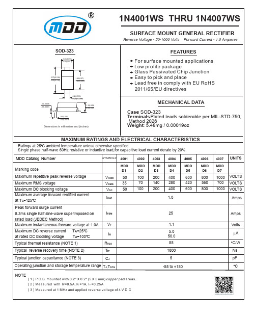
600 420 600
800 560 800
1000 700 1000
VOLTS VOLTS VOLTS Amps
IFSM VF IR RθJA Trr CJ
25 1.1 5.0 50.0 55 1800 5 -55 to +150
Amps Volts µA C/W Ns resistance (NOTE 1) Typical reverse recovery time (NOTE 2) Typical junction capacitance (NOTE 3)
Reverse Voltage (V)
Fig.5 Maximum Non-Repetitive Peak Forward Surage Current Peak Forward Surage Current (A)
40 35 30 25 20 15 10 5 00 1 10 100
8.3 ms Single Half Sine Wave (JEDEC Method)
Operating junction and storage temperature range TJ,TSTG NOTE
(1)P.C.B. mounted with 0.2" X 0.2" (5 X 5 mm) copper pad areas. (2)Measured with I F =0.5A,I R =1A , I rr = 0.25A (3)Measured at 1 MHz and applied reverse voltage of 4 V D.C
MDD Catalog Number
Marking code Maximum repetitive peak reverse voltage Maximum RMS voltage Maximum DC blocking voltage Maximum average forward rectified current at TC=125 C Peak forward surge current 8.3ms single half sine-wave superimposed on rated load (JEDEC Method) Maximum instantaneous forward voltage at 1.0A Maximum DC reverse current at rated DC blocking voltage TA=25 C TA=100 C
1N4007规格书
C
VR=-4VDC
15
ΡF
6.额定值曲线特性
23.4Min4.2~5.223.4 Min
主要材料/电镀
铜/镀锡( 7μmto 9μm)
2.印字
1. 阴极标志
2.型号名字1N4007
3. 数据标码WY
3.编带规格及包装
包装
KK
ΔS
SK:1.0mm
S:10.0±0.5mm
BΔS:1.2mm
B:6.0±1.0mm
GG:43.4±1.5mm
包装散装(非编带)1N4007-T
最大额定值内容符号额定单位最大反向电压vrrm1000v最大正向平均电流最大浪涌电流储存温度ifavifsm10aa300tjtstg651255
1N4007产品规格书
目录:
1.封装尺寸
2.印字
3.编带规格及包装
4.最大额定值
5.电性能参数
6.额定值曲线特性
张家港伟益电子有限公司
1.封装尺寸
φ0.6~0.7φ2.0~2.7
4.最大额定值
内容
符号
ห้องสมุดไป่ตู้额定
单位
最大反向电压
VRRM
1000
V
最大正向平均电流
IF(AV)
1.0
A
最大浪涌电流
IFSM
30.0
A
储存温度
Tj, Tstg
-65~+125
℃
5.电性能参数
内容
符号
条件
最大
单位
最大正向电压
VFM
IFM=1A
1.1
V
最大反向电流
IRRM
VTM=Rated Voltage
5
uA
N4007二极管

Features
Silicon Epitaxial Planar Switching Diode
PINNING PIN 1 2 DESCRIPTION Cathode Anode
2
• SOD-123 package • Fast switching • These diodes are also available in other case style including the DO-35 case with the type designation 1N4148, the MiniMELF case with the type designation 1N4007 and the MicroMELF case with the type designation MC1N4007.
Tj=100 C
Tj=25 C
0
1
2
VF (V)
Amissible power dissipation vs. ambient temperature 10
5
Leakage current vs. junction temperature
4
1000
800
2
103
5
P tot (mW)
I R (nA)
1
Top View Marking Code: " " Simplified outline SOD-123 and symbol
Absolute Maximum Ratings (Ta = 25 OC) Parameter Peak Reverse Voltage Reverse Voltage Average Rectified Forward Current Non-repetitive Peak Forward Surge Current at t = 1 μs Power Dissipation Thermal Resistance from Junction to Ambient Air Junction Temperature Storage Temperature Range
- 1、下载文档前请自行甄别文档内容的完整性,平台不提供额外的编辑、内容补充、找答案等附加服务。
- 2、"仅部分预览"的文档,不可在线预览部分如存在完整性等问题,可反馈申请退款(可完整预览的文档不适用该条件!)。
- 3、如文档侵犯您的权益,请联系客服反馈,我们会尽快为您处理(人工客服工作时间:9:00-18:30)。
Features
1N4001/L - 1N4007/L
1.0A RECTIFIER
“L” Suffix Designates A-405 Package No Suffix Designates DO-41 Package A
A
B C
D
DO-41 Plastic
A-405Dim Min Max Min Max A 25.40¾25.40¾B 4.06 5.21 4.10 5.20C 0.710.8640.530.64D
2.00
2.72
2.00
2.70
All Dimensions in mm
Maximum Ratings and Electrical Characteristics
@ T A = 25°C unless otherwise specified
·Diffused Junction
·High Current Capability and Low Forward Voltage Drop
·Surge Overload Rating to 30A Peak ·Low Reverse Leakage Current ·
Plastic Material: UL Flammability Classification Rating 94V-0
Mechanical Data
·Case: Molded Plastic
·Terminals: Plated Leads Solderable per MIL-STD-202, Method 208·Polarity: Cathode Band
·Weight: DO-41 0.30 grams (approx)
A-405 0.20 grams (approx)
·Mounting Position: Any ·
Marking: Type Number
Single phase, half wave, 60Hz, resistive or inductive load.For capacitive load, derate current by 20%.
Characteristic
Symbol 1N 4001/L 1N 4002/L 1N 4003/L 1N 4004/L
1N 4005/L 1N 4006/L 1N 4007/L Unit Peak Repetitive Reverse Voltage Working Peak Reverse Voltage DC Blocking Voltage V RRM
V RWM V R 501002004006008001000V RMS Reverse Voltage
V R(RMS)
35
70
140
280420
560
700
V Average Rectified Output Current (Note 1)@ T A = 75°C I O 1.0A Non-Repetitive Peak Forward Surge Current 8.3ms single half sine-wave superimposed on rated load (JEDEC Method)I FSM 30A Forward Voltage
@ I F = 1.0A V FM 1.0V Peak Reverse Current
@ T A = 25°C at Rated DC Blocking Voltage @ T A = 100°C
I RM 5.050
m A Typical Junction Capacitance (Note 2)
C j 15
8
pF Typical Thermal Resistance Junction to Ambient R q JA 100K/W Maximum DC Blocking Voltage Temperature T A +150°C Operating and Storage Temperature Range (Note 3)
T j,T STG
-65 to +175
°C
Notes:
1. Leads maintained at ambient temperature at a distance of 9.5mm from the case.
2. Measured at 1.MHz and applied reverse voltage of 4.0V DC.
3. JEDEC Value .
406080100120140160180
0.2
0.4
0.6
0.8
1.0
I ,A V E R A G E F O R W A R D R E C T I F I E D C U R R E N T (A )
(A V )T ,AMBIENT TEMPERATURE (ºC)Fig.1Forward Current Derating Curve
A C ,C A P A C I T A N C E (p F )
j V ,REVERSE VOLTAGE (V)Fig.4Typical Junction Capacitance
R 1.010
100
1.0
10
100
1.0
10100
I ,P E A
K F O R W A R D S U R G E C U R R E N T (A )
F S M NUMBER OF CYCLES AT 60Hz
Fig.3Max Non-Repetitive Peak Fwd Surge Current
40
30
20
010
500.6
0.8 1.0 1.2 1.4 1.6
0.01
0.1
1.0
I ,I N S T A
N T A N E O U S F O R W A R D C U R R E N T (A )
F V ,INSTANTANEOUS FORWARD VOLTAGE (V)
Fig.2Typical Forward Characteristics
F 10。