稳压二极管规格书资料
最全二极管资料手册

最全⼆极管资料⼿册⼀、常⽤BW系列稳压⼆极管参数与代换116种常⽤BW系列稳压⼆极管参数与代换116种型号最⼤耗散功率(W)稳定电压(V)最⼤⼯作电流(mA)可代换型号型号最⼤耗散功率(W)稳定电压(V)最⼤⼯作电流(mA)可代换型号BWA50A0.251832CW50.2CW50B,2CW9BWB39D0.53711.505W39V,2CW411,GY5-39BWA51A0.252.5712CW51B,2CW74010.605W43VBWA52A0.253.2552CWl1,2CW52,2CW52B BWB47D0.5449.71W46E,1W46G,1W46H,1W46FBWA530.254.25412CW53BBWB51D0.5488.91W53A,1W53B,1W53C,1W53DBW54/E0.255.5BWB56D0.5528.105W60VBWA55/E0.256.2331N709,2CW55,2CW55B BWB62D0.5587.32CW5264BWA560.257272CW15,2CW28-7.5,2CW56 BWB68D0.5646.705W75V,1/2W70-68V,1N6002 BWA57/E2CW28-9.1,2CW73BWB75D0.5706.11/2W80BWA58/E0.259.2232CW58A,2CW74,2CW74B BWB82D0.5775.51/2W90BWA59/E0.2510211N714,2CW18,2CW59 BWB91D0.5855.02CW526911.5192CW19,2CW60,2CW76A BWB100D0.5944.51/2W100BWA61/D/E0.2512.2161N716,2CW61,2CW77BBWB110D0.51044.11/2W110-110V,l/2W120,1N6025BWA62/D/E0.2513.5142CW20,2CW62B,2CW78 BWC50/D1380.2516132CW63,2DWI2H,2CW63B BWC51/D142181W50,2DW51BWA64/D/E0.2518112CW64B,2CW7KBWC52/D152151W60,2DW52BWA65/D0.2520101N721,2CW65,2DW12I BWC53/DBWA66/D0.252392CW20C,2CW65,2CW66 BWC54/D170111W80,2DW54BWA67/D0.252592CW67,2CW67BBWC55/D180101W90,2DW55BWA68/D0.252799091W100,2DW56BWA69/D0.252972CW69,2CW69BBWC57/D110081W110,2DW56-100V,2DW57BWA70/D0.253272CW70,2CW70B,2DW13C BWC58/D111071W120,2DW56-110V,2DW58BWA71/D0.252CW70C,2DW13DBWC59/D112061W130,2DW58-120V,2DW59BWA71E0.258.5252CW28-9.1,2CW57/BBWC60/D113561W140,2DW60BWA74E0.259.2232CW58/A/B,2CW74BWC61/D11456IW150,2DW6110212CW75B,2CW7HBWC62/D115551W160,2DW62BWA76E0.2511.5202CW19,2CW60/A,2CW76 BWC63/D116551W180,2DW63BWA77E0.2512.2182CW61,2CW61A,2CW77 BWC64/D11805BWA78E0.2513.5142CW20,2CW62/B,2CW78 BWC100A113302CW100,ZW100BWB2V40.52.2819105W2V4,2CW37-2.4,2CW382 BWC101A12.528020W101,ZW101BWB2V70.52.5016805W2V7,2CW37-2.7,2CW383 BWC1O212CW102,ZW1O2BWB3V00.52.815005W3V,2CW37-3.0,2CW384 BWCIO3/A141652CW103,2CW4V3,ZW103BWB3V30.53.113805W3V3,2CW37-3.3,BS73-3.3 BWC105/E16.21302CW105,1N4735BWB3V60.53.412605W3V6,2CW37-3.6,2CW3867.01102CW106,2DW2,BS63-7.5BWB3V90.53.711505W3V9,2CW37-3.9,2CW387 BWC1O7/E18.51002CW107,1N4739,2DW3BWB4V30.54.010605W4V3,2CW37-4.3,2CW21A BWClO9D/E110831N4740,2CW109,2DW5BWB4V70.54.4BWC110/D/E111.5762CW110,2CW138,ZW110BWB5V10.54.88905W5V1,2CW37-5.1,2CW390 BWC111/D/E112.2662CW111,ZW111BWB5V60.55.2812CW37-5.6,BS73-5.6,BZPD-5.6 BWC112/D/E113.5581W15V,2CW112,2CW286-15 BWB6V205W6V2,2CW37-6.2,2CW392 BWC113/D/E116522CW113,1N4745BWB6V80.56.46705W6V8,2CW37-6.8,2CW393 BWC114/D118472CW114,1N4746BWB7V50.57.0612CW21D,2CW37-7.5,2CW56 BWC115/D120412CW115,1N47477.75505W8V2,2CW37-8,22CW395 BWC116/D123382CW116,ZWl16BWB9V10.58.5502CW58,2CW73,2CW37-9.1 BWC117/D125352CW117,2W117BWB10E0.59.44605W10V,2CW37-10,2CW397 BWC118/D127BWB11E0.510.44005W11V,2CW37-11,2CW398 BWC119/D129302CW119,2W119BWB12D/E0.511.43805WI2V,2CW37-12,BS73-12 BWC12O/D132272CW120,ZWl20BWB13D/E0.512.4352CW400,BS73-13BWC121/D2CW121,ZW121BWB15D/E0.513.8302CW37-15,BS73-15 BWD80D333652CW149,2CW22NBWB16D/E0.515.3282CW37-16,BS73-16 BWD81D342502DW81,3W50BWB18D/E0.516.82552452DW82,3W80BWB20D/E0.518.82305W20V,2CW37-20,2CW404 BWD83D362402DW83,3W70BWB22D0.520.82105W22V,2CW37-22,2CW405 BWD84D370352DW84,3W80BWB24D0.505W24V,2CW406,RD24E BWD85D380302DW85,3W90BWB27D0.525.116.805W27V,2CW407,BZPD-27 BWD86D396252DW86BWB30D0.528.015.105W30V,2CW408,1N5255 BWD87D3100232DW87,3W1003113.805W33V,2CW409,W33A BWD88D3110202DW88,3W110BWB36D0.53412.605W36V,2CW410,2CW37-36 BWD89D3120202DW89,3W120型号最⼤耗散功率(W)稳定电压(V)最⼤⼯作电流(mA)可代换型号型号最⼤耗散功率(W)稳定电压(V)最⼤⼯作电流(mA)常⽤进⼝1N系列稳压⼆极管参数与代换90种型号最⼤耗散功率(W)稳定电压(V)最⼤⼯作电流(mA)可代换型号型号最⼤耗散功率(W)稳定电压(V)最⼤⼯作电流(mA)可代换型号1N5236/A/B0.57.5612CW105-7.5V,2CW52361N59870.531412CW51-3V,2CW52251N5237/A/B0.58.2552CW106-8.2V,2CW52373.31282CW51-3V3,2CW52261N5238/A/B0.58.7522CW106-8.7V,2CW5238 1N59890.53.61182GW51-3V6,2CW52271N5239/A/B0.59.1502CW107-9.1V,2CW5239 1N59900.53.91002CW52-3V9,2CW52281N5240/A/B0.5101N59910.54.3992CW52-4V3,2CW52291N5241/A/B0.511412CW109-11V,2CW5241 1N59920.54.7902CW53-4V7,2CW52301N5242/A/B0.512382CW11O-12V,2CW5242 1N59930.55.1832CW53-5V1,2CW5231 1N5243/A/B2CW111-13V,2CW5243 1N59940.55.6762CW53-5V6,2CW52321N5244/A/B0.514322CW111-14V,2CW5244 1N59950.56.2682CW54-6V2,2CW52341N5245/A/B0.515302CW112-15V,2CW5245 1N59960.56.8632CW54-6V8,2CW523516282CW112-16V,2CW5246 1N59970.57.5572CW55-7V5,2CW52361N5247/A/B0.517272CW113-17V,2CW5247 1N59980.58.2522CW55-8V2,2CW52371N5248/A/B0.518252CW113-l8V,2CW5248 1N59990.59.11N5249/A/B0.519242CW114-19V,2CW5249 1N60000.510432CW58-10V,2CW52401N5250/A/B0.520232CW114-20V,2CW5250 1N60010.511392CW59-11V,2CW52411N5251/A/B0.522212CW115-22V,2CW5251 1N60022CW60-12V,2CW52421N5252/A/B0.52419.12CW115-24V,2CW5252 IN60030.513332CW61-13V,2CW52431N5253/A/B0.52518.22CW116-25V,2CW5253 1N60040.515282CW62-15V,2CW52451N5254/A/B0.52716.816272GW62-16V,2CW52461N5255/A/B0.52816.22CW118-28V,2CW5255 1N60060.518242CW63-18V,2CW52481N5256/A/B0.53015.12CW119-30V,2CW5256 1N60070.520212CW64-20V,2CWS2SO1N5257/A/B0.52CW120-33V,2CW5257 1N60080.522192CW65-22V,2CW52511N57300.45.6652CW752IN60090.524182CW66-24V,2CW52521N57310.46.2622CW753,RD6.2EB1N60100.527162CW67-27V,2CW52546.8582CW754,2CW9571N60110.530142CW68-30V,2CW52561N57330.47.5522CW755,2CW9581N60120.533132CW69-33V,2CW52571N57340.48.2472CW756,2CW9591N60130.536121N57350.49.1422CW757,2CW9601N60140.539112CW71-39V,2CW52591N57360.410392CW758,2CW96l1N60150.5439.92CW72-43V,2GW52601N57370.411362CW9621N60160.50.5W47V,2CW52611N57380.412332CW7592,CW9631N60170.5518.30.5W51V,2CW52621N57390.413302CW760,2CW964,HZ-12C 1N60180.5567.60.5W56V,2CW52631N57400.415262CW965626.80.5W62V,2CW52651N57410.416242CW9661N60200.5686.30.5W68V,2CW52661N57420.418212CW9671N60210.5755.70.5W75V,2CW52671N57430.420IN60220.5825.20.5W82V,2CW52681N57440.422172GW9691N60230.5914.50.5W91V,2CW52701N57450.424152CW970,EQA02-25A 1N60240.51004.00.SW100V,2CW5271 1N57462CW971,HZS30E1N60250.51103.90.5W110V,2CW52721N57470.430112CW972,1/2W301N60260.51203.50.5W120V,2CW52731N57480.433102CW9731N60270.51303.30.5W130V3692CW9741N60280.51502.80.5W150V1N57500.43982CW9751N60290.51602.50.5W160V1N59850.52.41752CW50-2V4,2GW5221 1760300.51801N59860.52.71672CW50-2V7,2CW52231N60310.52001.00.5W200V型号最⼤耗散功率(W)稳定电压(V)最⼤⼯作电流(mA)可代换型号型号最⼤耗散功率(W)稳定电压(V)最⼤⼯作电流(mA)可代换型号常⽤进⼝BZ/EQ/BW系列稳压⼆极管参数与代换型号最⼤耗散功率(W)稳定电压(V)最⼤⼯作电流(mA)最⼤耗散功率(W)稳定电压(V)最⼤⼯作电流(mA)可代换型号BZPD-3.00.52.812505W3V、2CW384、2CW5224 EQA02-25A0.524~25181N5746、2CW971、HZS30EBZPD-3.30.53.111505W3V3、2CW37-3.3、HS73-3.3 EQA02-25C0.526~28152CW117、1N5254、2CW5254BZPD-3.60.505W3V6、2CW37-3.6、BS73-3.6 EQB01-05152002CW523、1N5231BZPD-3.90.53.89505W3V9、2CW37-3.9、2CW387 EQB01-06161802CW104、2CW5233BZPD-4.30.54.09005W4V3、2CW37-4.3、2CW388 EQB01-07171402CW105、2CW564.48505W4V7、2CW37-4.7、2CW389 EQBO1-08181202CW106、2CW134BZPD-5.10.54.88005W5V1、2CW37-5.1、2CW390 EQB01-09191102CW107、2CW135BZPD-5.60.55.2702CW37-5.6、BS73-5.6、2CW391 EQB01-10110100BZPD-6.20.55.86405W6V2、2CW37-6.2、2CW392 EQB01-11111902CW109、2CW137BZPD-6.80.56.45805W6V8、2CW37-6.8、2CW393 EQB01-12112802CW110、2CW138RZPD-7.50.57.0532CW56、2CW21D、BS73-7.5 EQB01-1312CW111、2CW139BZPD-8.20.57.74705W8V2、2CW37-8.2,2CW395 EQB01-14114702CW113A、2CW140-14VRZPD-9.10.58.5432CW37-9.1、2CW396EQB01-15115652CW113B、2CW14O-15VBZPD-100.59.4402CW37-10、05W10V、2CW39716602CW113C、2CW23A/BRZPD-110.510.43605W11V、2CW37-11、2CW398 EQB01-17117552CW114、2CW63-17VBZPD-120.511.43205W12V、2CW37-12、2CW399 EQB01-18118502GW114-18、2CW63-18VHZPD-130.512.4EQB0L-19119502CW114-19、2CW63-19VBZPD-150.513.8272CW37-15、RD15E,2CW401 EQB01-20120452CW115-20、2CW64-20VBZPD-160.515.3242CW37-16、BS73-16、2CW402 EQB01-21121452CW115-21、2CW64-21V BZPD-182CW37-18、RS73-18,2CW403 EQB01-22122402CW115-22、2CW64-22VBZPD-200.518.8202CW37-20,05W20V、2CW404 EQB01-23123402CW116-23、2CW144-23VBZPD-220.520.81805W22V、2CW37-22,2CW405 EQB01-24124402CW116-24、2C525222.71605W24V,RD24E、2CW406 EQB01-25125402CW116-25、2CW145-25VBZPD-270.525.11405W27V、RD27E、2CW407 EQB0l-26126352CW117-26、2CW145-26VRZXC5V10.54.88005W5V1、2CW37-5.1、2CW390 EQB01-28128BZXC7V50.57.5702CW5236、2CW55-7V5 EQB01-30130302CW118-30、2CW147-30VBZXC120.512402CW77、2CW61AEQB01-3213230µPC574,TAA550BZX79B5V0.45752CW13、05W5V1BWD90D2DW90、3W140RZX79B6V80.46.8552CW55A、1N71O BWD130336602CW130、2CW22BZX79B36V0.436102CW120-36V、BWC50D BWD131345002CW131、2CW22ABZX79C6V20.46.2605.54602CW132、2CW22BBZX79C200.420202CW23B、2CW23CBWD13336.24002CW133、2CW22CBZX83-150.513.8272CW37-15、BS73-15、RD15E BWD13437.03302CW134、2CW22DBZX83-5V10.5。
ST10BC稳压二极管规格书
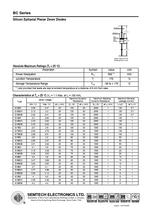
1)
Maximum Dynamic Resistance at lZT (mA) 20 20 20 20 20 20 20 20 20 20 20 20 20 20 20 20 20 20 20 20 20 20 20 20 ZZT (Ω) 120 120 120 100 100 100 100 100 100 80 80 80 70 70 70 60 60 60 50 50 50 40 40 40 at lZT (mA) 20 20 20 20 20 20 20 20 20 20 20 20 20 20 20 20 20 20 20 20 20 20 20 20
Maximum Reverse Leakage Current IR (µA) 5 5 5 5 5 5 5 5 5 5 5 5 5 5 5 5 5 2 2 2 2 0.5 0.5 0.5 0.5 0.5 0.5 0.5 0.5 0.5 0.5 0.5 0.5 0.2 0.2 0.2 0.2 0.2 0.2 0.2 0.2 0.2 0.2 0.2 0.2 0.2 at VR (V) 1 1 1 1 1 1.5 1.5 1.5 1.5 2.5 2.5 2.5 2.5 3 3 3 3 3.5 3.5 3.5 3.5 4 4 4 4 5 5 5 5 6 6 6 6 7 7 7 7 8 8 8 8 9 9 9 9 10
稳压二极管1n4735a的数据手册
稳压二极管1n4735a的数据手册
稳压二极管是一种常见的电子元件,它可以将电压稳定在一个特定的范围内,从而保护电路中的其他元件。
1n4735a是一种常见的稳压二极管,本文将介绍它的数据手册。
一、外观和尺寸
1n4735a的外观为圆柱形,尺寸为直径4.3mm,高度9.5mm。
它的引脚为两个金属引脚,引脚间距为2.54mm。
二、电性能参数
1n4735a的最大反向电压为6.2V,最大正向电流为1W。
它的稳定电压为5.1V,稳定电流为37mA。
在这些参数下,1n4735a的最大功耗为400mW。
三、特性曲线
1n4735a的特性曲线是指在不同电流下,其电压与电流的关系曲线。
在稳定电流下,1n4735a的电压变化很小,可以保证电路中其他元件的工作稳定。
四、应用
1n4735a广泛应用于各种电子设备中,如电源、稳压器、逆变器等。
它
可以保护电路中其他元件不受过高或过低的电压影响,从而提高电路
的可靠性和稳定性。
五、注意事项
在使用1n4735a时,需要注意以下几点:
1. 1n4735a的最大功耗为400mW,不能超过这个值,否则会损坏元件。
2. 在使用1n4735a时,需要根据实际需要选择合适的稳定电压和稳定
电流。
3. 在焊接1n4735a时,需要注意温度和时间,避免过高的温度和过长
的时间导致元件损坏。
总之,1n4735a是一种常见的稳压二极管,具有稳定电压、稳定电流等
优良特性,广泛应用于各种电子设备中。
在使用时需要注意功耗、稳
定电压和稳定电流等参数,以及焊接温度和时间等细节。
稳压二极管bzt52c参数
稳压二极管BZT52C参数1. 引言稳压二极管(Zener Diode)是一种特殊的PN结二极管,主要用于电源稳压和电压参考。
BZT52C是一种常见的稳压二极管型号,本文将对其参数进行详细介绍。
2. BZT52C概述BZT52C是一种表面贴装稳压二极管,采用玻璃封装。
它具有快速响应、可靠性高、功耗低等特点,广泛应用于电子设备中。
3. 参数说明3.1 额定功率额定功率是指在规定条件下,稳压二极管能够持续工作的最大功率。
对于BZT52C系列而言,其额定功率通常为0.5W。
3.2 额定电流额定电流是指在规定条件下,稳压二极管能够承受的最大电流。
对于BZT52C系列而言,其额定电流通常为200mA。
3.3 工作温度范围工作温度范围指的是稳压二极管能够正常工作的温度范围。
对于BZT52C系列而言,其工作温度范围通常为-65°C至+150°C。
3.4 稳定电压稳定电压是指稳压二极管在正向工作时,其两端的电压保持相对恒定的值。
对于BZT52C系列而言,其稳定电压通常为3.3V或5.1V。
3.5 动态电阻动态电阻是指稳压二极管在正向工作时,其两端电压变化一个单位时所引起的电流变化。
对于BZT52C系列而言,其动态电阻通常在5Ω以下。
4. BZT52C应用4.1 电源稳压由于BZT52C具有稳定的特性,可以用作电源稳压元件。
当输入电压波动时,BZT52C能够保持输出电压恒定,有效保护后续电路不受过高或过低的输入电压影响。
4.2 参考电压源由于BZT52C具有固定的稳定电压值,因此可以用作参考电压源。
通过合适的接线和外部元件配合使用,可以实现精确的参考电压输出。
4.3 限流保护BZT52C在正向工作时具有较低的电阻,可以起到限流保护的作用。
当电路中出现过流时,BZT52C会自动调整其两端的电压,从而限制电流的大小。
5. BZT52C选型建议5.1 根据稳定电压需求选择型号根据实际应用需求,选择合适的BZT52C型号。
MM5Z18VT1G稳压二极管规格书
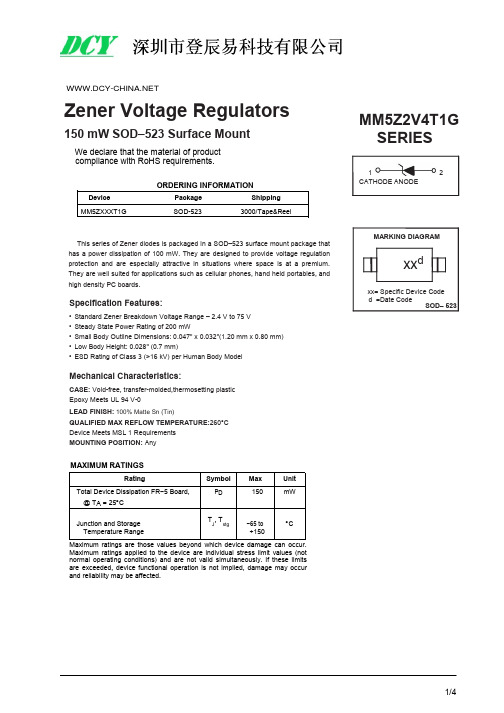
Zener Voltage Regulators150mW SOD–523Surface MountWe declare that the material of product compliance with RoHS requirements.ORDERING INFORMATIONDevice Package Shipping MM5ZXXXT1GSOD-5233000/Tape&ReelThis series of Zener diodes is packaged in a SOD–523surface mount package that has a power dissipation of 100mW.They are designed to provide voltage regulation protection and are especially attractive in situations where space is at a premium.They are well suited for applications such as cellular phones,hand held portables,and high density PC boards.Specification Features:•Standard Zener Breakdown Voltage Range –2.4V to 75V •Steady State Power Rating of 200mW•Small Body Outline Dimensions:0.047"x 0.032"(1.20mm x 0.80mm)•Low Body Height:0.028"(0.7mm)•ESD Rating of Class 3(>16kV)per Human Body ModelMechanical Characteristics:CASE:Void-free,transfer-molded,thermosetting plastic Epoxy Meets UL 94V-0LEAD FINISH:100%Matte Sn (Tin)QUALIFIED MAX REFLOW TEMPERATURE:260°C Device Meets MSL 1Requirements MOUNTING POSITION:AnyMAXIMUM RATINGSRatingSymbol Max Unit Total Device Dissipation FR−5Board,P D150mW@T A =25︒C Junction and Storage T J,Tstg−65to ︒CTemperature Range+150Maximum ratings are those values beyond which devicedamage can occur.Maximum ratings applied to the device are individual stress limit values (not normal operating conditions)and are not valid simultaneously.If these limits are exceeded,device functional operation is not implied,damage may occur and reliability may be affected.MM5Z2V4T1G SERIES12CATHODE ANODEMARKING DIAGRAMxx dxx=Specific Device Code d =Date CodeSOD–523MM5Z2V4T1G SERIES ELECTRICAL CHARACTERISTICS I(T A=25︒C unless otherwise noted,I FV F=0.9V Max.@I F=10mA for all types)Symbol ParameterVZ Reverse Zener Voltage@I ZT IZT Reverse Current VZVRVZ ZT Maximum Zener Impedance@I I R VFZT IZTIZK Reverse CurrentZZK Maximum Zener Impedance@I ZKIR Reverse Leakage Current@V RV R Reverse VoltageI F Forward Current Zener Voltage Regulator V F Forward Voltage@I FQV Z Maximum Temperature Coefficient of V ZC Max.Capacitance@V R=0and f=1MHz100(%)80DISS IP ATI ON 60 40POWER20255075100125150TEMPERATURE(︒C)Figure1.Steady State Power Derating MM5Z2V4T1G SERIESELECTRICAL CHARACTERISTICS (T A =25︒C unless otherwise noted,V F =0.9V Max.@I F =10mA for all types)Zener Voltage (Note 1)Zener Impedance Leakage CurrentQ V Z C ZZT(mV/k)@V =0V(Volts)@I@I ZT Z@II @VRZZKR@IZTf =1MHzDevice ZTZKRDevice Marking Min Nom Max mA W W mA m A Volts Min Max pF MM5Z2V4T1G 00 2.2 2.4 2.651001000 1.050 1.0−3.50450MM5Z2V7T1G 01 2.5 2.7 2.951001000 1.020 1.0−3.50450MM5Z3V0T1G 02 2.8 3.0 3.251001000 1.010 1.0−3.50450MM5Z3V3T1G 05 3.1 3.3 3.55951000 1.05 1.0−3.50450MM5Z3V6T1G 06 3.4 3.6 3.85901000 1.05 1.0−3.50450MM5Z3V9T1G 07 3.7 3.9 4.15901000 1.03 1.0−3.5−2.5450MM5Z4V3T1G 08 4.0 4.3 4.65901000 1.03 1.0−3.50450MM5Z4V7T1G 09 4.4 4.7 5.0580800 1.03 2.0−3.50.2260MM5Z5V1T1G 0A 4.8 5.1 5.4560500 1.02 2.0−2.7 1.2225MM5Z5V6T1G 0C 5.2 5.6 6.0540400 1.01 2.0−2.0 2.5200MM5Z6V2T1G 0E 5.8 6.2 6.6510100 1.03 4.00.4 3.7185MM5Z6V8T1G 0F 6.4 6.87.2515160 1.02 4.0 1.2 4.5155MM5Z7V5T1G 0G 7.07.57.9515160 1.01 5.0 2.5 5.3140MM5Z8V2T1G 0H 7.78.28.7515160 1.00.7 5.0 3.2 6.2135MM5Z9V1T1G 0K 8.59.19.6515160 1.00.27.0 3.87.0130MM5Z10VT1G 0L 9.41010.6520160 1.00.18.0 4.58.0130MM5Z11VT1G 0M 10.41111.6520160 1.00.18.0 5.49.0130MM5Z12VT1G 0N 11.41212.752580 1.00.18.0 6.010130MM5Z13VT1G 0P 12.413.2514.153080 1.00.18.07.011120MM5Z15VT1G 0T 14.31515.8530200 1.00.0510.59.213110MM5Z16VT1G 0U 15.316.217.1240200 1.00.0511.210.414105MM5Z18VT1G 0W 16.81819.1245225 1.00.0512.612.416100MM5Z20VT1G 0Z 18.82021.2255225 1.00.0514.014.41885MM5Z22VT1G 1020.82223.3255250 1.00.0515.416.42085MM5Z24VT1G 1122.824.225.6270120 1.00.0516.818.42280MM5Z27VT1G 1225.12728.9280300 1.00.0518.921.425.370MM5Z30VT1G 14283032280300 1.00.0521.024.429.470MM5Z33VT1G 18313335280300 1.00.0523.227.433.470MM5Z36VT1G 19343638290500 1.00.0525.230.437.470MM5Z39VT1G 203739412130500 1.00.0527.333.441.245MM5Z43VT1G 214043461150500 1.00.0530.137.646.640MM5Z47VT1G 1A 4447501170500 1.00.0532.942.051.840MM5Z51VT1G 1C 4851541180500 1.00.0535.746.657.240MM5Z56VT1G 1D 5256601200500 1.00.0539.252.263.840MM5Z62VT1G 1E 5862661215500 1.00.0543.458.871.635MM5Z68VT1G 1F 6468721240500 1.00.0547.665.679.835MM5Z75VT1G1G70757912555001.00.0552.573.488.6351.Zener voltage is measured with a pulse test current I Z at an ambient temperature of 25︒C.MM5Z2V4T1G SERIESSC-79/SOD-523DIMENSIONS (mm are the original dimensions)UNIT A b p c D E H E V m m0.70.350.2 1.30.9 1.70.150.50.250.11.10.71.5Note1.The marking bar indicates the cathode.OUTLINE REFERENCES EUROPEAN ISSUE DATEVERSION IECJEDECEIAJ PROJECTIONSOD523SC-7998-11-25。
MM3Z15VT1G稳压二极管规格书

Zener Voltage Regulators200 mW SOD–323 Surface MountMM3Z2V0T1GSeriesThis series of Zener diodes is packaged in a SOD–323 surface mount package that has a power dissipation of 200 mW. They are designed to provide voltage regulation protection and are especially attractive in situations where space is at a premium. They are well suited for applications such as cellular phones, hand held portables, and high density PC boards.Specification Features:• Standard Zener Breakdown Voltage Range – 2.0 V to 75 V • Steady State Power Rating of 200 mW• Small Body Outline Dimensions: 0.067" x 0.049"(1.7 mm x 1.25 mm).Low Body Height: 0.035" (0.9 mm)• Package Weight: 4.507mg/unit• ESD Rating of Class 3 per Human Body Model • Pb-Free package is available.Mechanical Characteristics:CASE:Void-free, transfer-molded plasticFINISH:All external surfaces are corrosion resistant260°C for 10 SecondsPOLARITY:Cathode indicated by polarity band FLAMMABILITY RATING: UL94 V-0MOUNTING POSITION: AnyMAXIMUM RATINGSRating SymbolMax UnitTotal Device Dissipation FR–5 P DBoard(Note 1.) @ TA = 25°C 200 mW Derate above 25°C 1.5mW/°C Thermal Resistance fromR θJA635 °C/W Junction to Ambient Junction and StorageT J , T stg –65 to+150 °CTemperature Range 1. FR–4 Minimum PadDevicePackageShippingMM3Z2V0T1G Series SOD-3233000/Tape&ReelMM3Z2V0T3G SeriesSOD-32310000/Tape&ReelRev.A 1/6• S- Prefix for Automotive and Other Applications Requiring Unique Site and Control Change Requirements; AEC-Q101 Qualified and PPAP Capable.• We declare that the material of product compliance with RoHS requirements.ORDERING INFORMATIONMaximum case temperature for soldering purpose:MM3Z2V0T1G SeriesELECTRICAL CHARACTERISTICS(T A = 25°C unless otherwise noted,V F = 0.9 V Max. @ IF = 10 mA for all types)Symbol ParameterV Z Reverse Zener Voltage @ I ZT I ZT Reverse CurrentZ ZT Maximum Zener Impedance @ I ZT I ZK Reverse CurrentZ ZK Maximum Zener Impedance @ I ZK I R Reverse Leakage Current @ V R V R Reverse Voltage I F Forward Current V F Forward Voltage @ I FQ V Z Maximum Temperature Coefficient of V Z CMax. Capacitance @V R = 0 and f = 1 MHzRev.A 2/62.Zener voltage is measured with a pulse test current I Z at an ambient temperature of 25°C.Rev.A 3/6MM3Z2V0T1G SeriesTypical CharacteristicsZ Z T , D Y N A M I C I M P E D A N C E ()Ω1000100101.0C , C A P A C I T A N C E (p F )70V Z , NOMINAL ZENER VOLTAGE (V)Figure 3. Typical Capacitance 104.0V Z , NOMINAL ZENER VOLTAGE (V)Figure 4. Typical Leakage Current70605040302010Rev.A 4/6MM3Z2V0T1G SeriesTypical Characteristics12V Z , ZENER VOLTAGE (V)100101.00.10.01108.06.04.02.00I Z , Z E N E R C U R R E N T (m A )V Z , ZENER VOLTAGE (V)Figure 5. Zener Voltage versus Zener Current(V Z Up to 12 V)Figure 6. Zener Voltage versus Zener Current(12 V to 75 V)1001010.10.011030507090I Z , Z E N E R C U R R E N T (m A )Figure 7. Steady State Power DeratingRev.A 5/6300200100005025100150P O W E R D I S S I P A T I O N : P d (m W )AMBIENT TEMPERA TURE : T a (°C)MM3Z2V0T1G SeriesPACKAGE DIMENSIONSSOD-323Rev.A 6/6HE NOTES:1.DIMENSIONING AND TOLERANCING PER ANSI Y14.5M, 1982.2.CONTROLLING DIMENSION: MILLIMETERS.3.LEAD THICKNESS SPECIFIED PER L/F DRAWING WITH SOLDER PLATING.4.DIMENSIONS A AND B DO NOT INCLUDE MOLD FLASH, PROTRUSIONS OR GATE BURRS.5.DIMENSION L IS MEASURED FROM END OF RADIUS.NOTE 3DIM MIN NOM MAX MILLIMETERSA 0.800.90 1.00A10.000.050.10A30.15 REF b 0.250.320.4C 0.0890.120.177D 1.60 1.70 1.80E 1.15 1.25 1.350.082.30 2.50 2.70L 0.0310.0350.0400.0000.0020.0040.006 REF0.0100.0120.0160.0030.0050.0070.0620.0660.0700.0450.0490.0530.0030.0900.0980.105MINNOM MAX INCHESSOLDERING FOOTPRINT*MM3Z2V0T1G Series。
教你读稳压二极管的规格书
教你读稳压二极管的规格书主要参数
以《1SMB5942B-_1N5921B-1N5942B》PANJIT 台湾强茂稳压二极管规格书介绍
ON的稳压二极管逐步停产,公司选用了台湾强茂电子的二极管。
主要参数:
Vz 标称稳压值,以1SMB5923B为了,Vz=8.2V , Vz 有最小值7.79V ,最大值8.61V .
Izt 表示在标称稳压值8.2V下的电流值,为45.7mA。
Zzt 表示在标称稳压值8.2V 和标称稳压电流值45.7m A下的稳压二极管阻抗,该值为4 Ω。
Izk 表示稳压二极管反向击穿拐点处的电流。
Zzk 表示稳压二极管反向击穿拐点处的阻抗。
稳压二极管的阻抗随着电流的增大而减小,阻抗Zz 与电流Iz 基本上有一个反比例的关系。
V R表示稳压二极管的反向电压(对于稳压二极管来说的反向电压,相当于其他普通二极管就是正向电压)。
I R表示稳压二极管在反向电压6.5V 情况下的漏电流为5u A .
另外,热耗散功率P D为1.5W ,注意功率不能超过1.5W,否则会烧坏该二极管。
MM3Z3V3T1G稳压二极管规格书
Zener Voltage Regulators200 mW SOD–323 Surface MountMM3Z2V0T1GSeriesThis series of Zener diodes is packaged in a SOD–323 surface mount package that has a power dissipation of 200 mW. They are designed to provide voltage regulation protection and are especially attractive in situations where space is at a premium. They are well suited for applications such as cellular phones, hand held portables, and high density PC boards.Specification Features:• Standard Zener Breakdown Voltage Range – 2.0 V to 75 V • Steady State Power Rating of 200 mW• Small Body Outline Dimensions: 0.067" x 0.049"(1.7 mm x 1.25 mm).Low Body Height: 0.035" (0.9 mm)• Package Weight: 4.507mg/unit• ESD Rating of Class 3 per Human Body Model • Pb-Free package is available.Mechanical Characteristics:CASE:Void-free, transfer-molded plasticFINISH:All external surfaces are corrosion resistant260°C for 10 SecondsPOLARITY:Cathode indicated by polarity band FLAMMABILITY RATING: UL94 V-0MOUNTING POSITION: AnyMAXIMUM RATINGSRating SymbolMax UnitTotal Device Dissipation FR–5 P DBoard(Note 1.) @ TA = 25°C 200 mW Derate above 25°C 1.5mW/°C Thermal Resistance fromR θJA635 °C/W Junction to Ambient Junction and StorageT J , T stg –65 to+150 °CTemperature Range 1. FR–4 Minimum PadDevicePackageShippingMM3Z2V0T1G Series SOD-3233000/Tape&ReelMM3Z2V0T3G SeriesSOD-32310000/Tape&ReelRev.A 1/6• S- Prefix for Automotive and Other Applications Requiring Unique Site and Control Change Requirements; AEC-Q101 Qualified and PPAP Capable.• We declare that the material of product compliance with RoHS requirements.ORDERING INFORMATIONMaximum case temperature for soldering purpose:MM3Z2V0T1G SeriesELECTRICAL CHARACTERISTICS(T A = 25°C unless otherwise noted,V F = 0.9 V Max. @ IF = 10 mA for all types)Symbol ParameterV Z Reverse Zener Voltage @ I ZT I ZT Reverse CurrentZ ZT Maximum Zener Impedance @ I ZT I ZK Reverse CurrentZ ZK Maximum Zener Impedance @ I ZK I R Reverse Leakage Current @ V R V R Reverse Voltage I F Forward Current V F Forward Voltage @ I FQ V Z Maximum Temperature Coefficient of V Z CMax. Capacitance @V R = 0 and f = 1 MHzRev.A 2/62.Zener voltage is measured with a pulse test current I Z at an ambient temperature of 25°C.Rev.A 3/6MM3Z2V0T1G SeriesTypical CharacteristicsZ Z T , D Y N A M I C I M P E D A N C E ()Ω1000100101.0C , C A P A C I T A N C E (p F )70V Z , NOMINAL ZENER VOLTAGE (V)Figure 3. Typical Capacitance 104.0V Z , NOMINAL ZENER VOLTAGE (V)Figure 4. Typical Leakage Current70605040302010Rev.A 4/6MM3Z2V0T1G SeriesTypical Characteristics12V Z , ZENER VOLTAGE (V)100101.00.10.01108.06.04.02.00I Z , Z E N E R C U R R E N T (m A )V Z , ZENER VOLTAGE (V)Figure 5. Zener Voltage versus Zener Current(V Z Up to 12 V)Figure 6. Zener Voltage versus Zener Current(12 V to 75 V)1001010.10.011030507090I Z , Z E N E R C U R R E N T (m A )Figure 7. Steady State Power DeratingRev.A 5/6300200100005025100150P O W E R D I S S I P A T I O N : P d (m W )AMBIENT TEMPERA TURE : T a (°C)MM3Z2V0T1G SeriesPACKAGE DIMENSIONSSOD-323Rev.A 6/6HE NOTES:1.DIMENSIONING AND TOLERANCING PER ANSI Y14.5M, 1982.2.CONTROLLING DIMENSION: MILLIMETERS.3.LEAD THICKNESS SPECIFIED PER L/F DRAWING WITH SOLDER PLATING.4.DIMENSIONS A AND B DO NOT INCLUDE MOLD FLASH, PROTRUSIONS OR GATE BURRS.5.DIMENSION L IS MEASURED FROM END OF RADIUS.NOTE 3DIM MIN NOM MAX MILLIMETERSA 0.800.90 1.00A10.000.050.10A30.15 REF b 0.250.320.4C 0.0890.120.177D 1.60 1.70 1.80E 1.15 1.25 1.350.082.30 2.50 2.70L 0.0310.0350.0400.0000.0020.0040.006 REF0.0100.0120.0160.0030.0050.0070.0620.0660.0700.0450.0490.0530.0030.0900.0980.105MINNOM MAX INCHESSOLDERING FOOTPRINT*MM3Z2V0T1G Series。
117稳压管规格书
117稳压管规格书【原创实用版】目录1.117 稳压管概述2.117 稳压管规格参数3.117 稳压管的工作原理4.117 稳压管的应用领域5.117 稳压管的安装与使用注意事项正文一、117 稳压管概述117 稳压管,又称为 117 型号稳压二极管,是一种用于电子电路中的稳压元件。
它可以将输入电压稳定在一定的范围内,以保证电子设备在各种电压波动的情况下仍能正常工作。
117 稳压管在我国电子行业中应用广泛,其性能稳定、可靠性高,成为众多电子工程师的首选稳压元件。
二、117 稳压管规格参数117 稳压管的规格参数主要包括以下几个方面:1.额定电压:117 稳压管的额定电压一般在 3.0-4.5V 之间,也有部分特殊型号的稳压管额定电压可以达到更高的值。
2.动态电阻:动态电阻是指稳压管在稳定电压状态下,其两端的电压变化与电流变化的比值。
117 稳压管的动态电阻通常在几欧姆到几十欧姆之间。
3.漏电流:漏电流是指在 117 稳压管两端电压为零时,流经稳压管的电流。
漏电流越小,稳压管的性能越优秀。
4.功率:117 稳压管的功率主要取决于其额定电压和电流,通常在几十毫瓦到几百毫瓦之间。
三、117 稳压管的工作原理117 稳压管的工作原理基于半导体材料的 PN 结,当外加电压达到其额定电压时,PN 结会被正向导通,从而使得电路中的电流稳定。
当输入电压超过其额定电压时,117 稳压管会吸收多余的电压,使得输出电压保持稳定。
反之,当输入电压低于其额定电压时,117 稳压管会提供额外的电压,以保证输出电压的稳定。
四、117 稳压管的应用领域117 稳压管广泛应用于各种电子设备和电路中,例如:电源适配器、充电器、电视机、收音机、通信设备等。
在这些设备中,117 稳压管起到了稳定电压、保护电路的作用,确保设备在各种电压波动的情况下仍能正常工作。
五、117 稳压管的安装与使用注意事项1.在安装 117 稳压管时,应注意将其插入电路板时,电极朝向应与电路板设计一致,避免插反。
SOD-123型号的塑封稳压二极管商品说明书
SOD-123贴片塑封稳压二极管SOD-123 Plastic-Encapsulate Zener Diode特征Featuresz 齐纳击穿阻抗低; Low Zener Impedancez 最大功率耗散500mW; Power Dissipation of 500mW z 高稳定性和可靠性。
High Stability and High Reliability 机械数据Mechanical DataSOD-123z 封装: SOD-123封装SOD-123 Small Outline Plastic Package z 极性: 色环端为负极Polarity: Color band denotes cathode end z 环氧树脂UL 易燃等级Epoxy UL: 94V-0 z安装位置: 任意Mounting Position: Any极限值和温度特性(TA = 25℃ 除非另有规定)Maximum Ratings & Thermal Characteristics (Ratings at 25℃ ambient temperature unless otherwise specified.) 参数 Parameters符号Symbol 数值Value 单位Unit功率消耗Power DissipationPd 500 mW正向压降Forward Voltage @IF=10mA Vf 0.9 V存储温度Storage temperature rangeTs -65-+150℃ 1) Device mounted on ceramic PCB: 7.6mm x 9.4mm x 0.87mm with pad areas 25mm²2) Short duration test pulse used to minimize self-heating effect 3)f=1KHz电特性 (TA = 25℃ 除非另有规定)Electrical Characteristics (Ratings at 25℃ ambient temperature unless otherwise specified).Zener Voltage RangeMaximum Zener Impedance MaximumReverse CurrentVz@Izt IztZzt @Izt Zzk @IzkIzk IR VRTypicalTemperaturecoefficent @IZTC=mV/℃TestCurrentIZTC Device MarkingNom(V) Min(V) Max(V) mA Ω mAuA V Min Max mA BZT52B2V4 2WX 2.4 2.35 2.45 5 100 600 1.050 1.0 -3.5 0 5 BZT52B2V7 2W1 2.7 2.65 2.75 5 100 600 1.020 1.0 -3.5 0 5 BZT52B3V0 2W2 3.0 2.94 3.06 5 95 600 1.010 1.0 -3.5 0 5 BZT52B3V3 2W3 3.3 3.23 3.37 5 95 600 1.0 5 1.0 -3.5 0 5 BZT52B3V6 2W4 3.6 3.53 3.67 5 90 600 1.0 5 1.0 -3.5 0 5 BZT52B3V9 2W5 3.9 3.82 3.98 5 90 600 1.0 3 1.0 -3.5 0 5 BZT52B4V3 2W6 4.3 4.21 4.39 5 90 600 1.0 3 1.0 -3.5 05BZT52B4V7 2W7 4.7 4.61 4.79 5 80 500 1.0 3 2.0 -3.5 0.2 5 BZT52B5V1 2W8 5.1 5.00 5.20 5 60 480 1.0 2 2.0 -2.7 1.2 5 BZT52B5V6 2W9 5.6 5.49 5.71 5 40 400 1.0 1 2.0 -2.0 2.5 5 BZT52B6V2 2WA 6.2 6.08 6.32 5 10 150 1.0 3 4.0 0.4 3.7 5 BZT52B6V8 2WB 6.8 6.66 6.94 5 15 80 1.0 2 4.0 1.2 4.5 5 BZT52B7V5 2WC 7.5 7.35 7.65 5 15 80 1.0 15.0 2.5 5.3 5BZT52B8V2 2WD 8.2 8.04 8.36 5 1580 1.00.7 5.0 3.2 6.2 5 BZT52B9V1 2WE 9.1 8.929.28 5 15 100 1.00.5 6.0 3.8 7.0 5 BZT52B10 2WF 10 9.80 10.20 5 20 150 1.00.2 7.0 4.5 8.0 5 BZT52B11 2WG 11 10.78 11.22 5 20 150 1.00.1 8.0 5.4 9.0 5 BZT52B12 2WH 12 11.76 12.24 5 25 150 1.00.1 8.0 6.0 10.0 5 BZT52B13 2WI 13 12.74 13.26 5 30 170 1.00.1 8.0 7.0 11.051) 2)Zener Voltage RangeMaximum Zener Impedance MaximumReverse CurrentVz@Izt Izt Zzt @Izt Zzk @IzkIzkIR VRTypicalTemperaturecoefficent @IZTC=mV/℃TestCurrentIZTC Device MarkingNom(V) Min(V) Max(V) mA Ω mAuA V Min Max mABZT52B15 2WJ 15 14.70 15.30 5 30 200 1.00.1 10.5 9.2 13.0 5 BZT52B16 2WK 16 15.68 16.32 5 40 200 1.00.1 11.2 10.4 14.0 5 BZT52B18 2WL 18 17.64 18.36 5 45 225 1.00.1 12.6 12.4 16.0 5 BZT52B20 2WM 20 19.60 20.40 5 55 225 1.00.1 14.0 14.4 18.0 5 BZT52B22 2WN 22 21.56 22.44 5 55 250 1.00.1 15.4 16.4 20.0 5 BZT52B24 2WO 24 23.52 24.48 5 70 250 1.00.1 16.8 18.4 22.0 5 BZT52B27 2WP 27 26.46 27.54 2 80 300 0.50.1 18.9 21.4 25.3 2 BZT52B30 2WQ 30 29.40 30.60 2 80 300 0.50.1 21.0 24.4 29.4 2 BZT52B33 2WR 33 32.34 33.66 2 80 325 0.50.1 23.1 27.4 33.4 2 BZT52B36 2WS 36 35.28 36.72 2 90 350 0.50.1 25.2 30.4 37.4 2 BZT52B39 2WT 39 38.22 39.78 2 130 350 0.50.1 27.3 33.4 41.2 2 BZT52B43 2WU 43 41.16 43.84 2 100 700 1.00.1 32.0 10.0 12.0 5 BZT52B47 2WV 47 46.06 47.94 2 100 750 1.00.1 35.0 10.0 12.0 5 BZT52B51 2WW 51 49.98 52.02 2 100 750 1.00.1 38.0 10.0 12.05Breakdown characteristicsat Tj=constant (pulsed)Forward characteristicsAdmissible power dissipation versus ambient temperaturePulse thermal resistance versus pulse durationDynamic resistance versus Zener currentCapacitance versus Zener voltageDynamic resistance versus Zener current Dynamic resistance versus Zener current Thermal differential resistance versus Zener voltageDynamic resistance versus Zener voltageTemperature dependence of Zener voltage versus Zener voltageTemperature dependence of Zener voltage versus Zener voltageChange of Zener voltage versus junction temperatureChange of Zener voltage versus junction temperatureChange of Zener voltge from turn-on up to the point of thermalequilibrium versus Zener voltageSOD-123 PACKAGE OUTLINE Plastic surface mounted package焊盘设计参考Precautions: PCB DesignRecommended land dimensions for SOD-123 diode. Electrode patterns for PCBs中心距: 3.24 脚宽: 0.55 焊盘宽: 1.00 脚长: 0.50 焊盘长: 0.80 技术要求:1, 塑封体尺寸: 2.70 X 1.60 2: 未注公差为: ±0.053, 所有单位: mm。
- 1、下载文档前请自行甄别文档内容的完整性,平台不提供额外的编辑、内容补充、找答案等附加服务。
- 2、"仅部分预览"的文档,不可在线预览部分如存在完整性等问题,可反馈申请退款(可完整预览的文档不适用该条件!)。
- 3、如文档侵犯您的权益,请联系客服反馈,我们会尽快为您处理(人工客服工作时间:9:00-18:30)。
MMSZ5221BT1 SeriesPreferred DeviceZener Voltage Regulators 500 mW SOD−123 Surface MountThree complete series of Zener diodes are offered in the convenient, surface mount plastic SOD−123 package. These devices provide a convenient alternative to the leadless 34−package style.Features•500 mW Rating on FR−4 or FR−5 Board•Wide Zener Reverse V oltage Range − 2.4 V to 110 V •Package Designed for Optimal Automated Board Assembly •Small Package Size for High Density Applications •General Purpose, Medium Current•ESD Rating of Class 3 (>16 kV) per Human Body Model•Pb−Free Packages are AvailableMechanical CharacteristicsCASE:V oid-free, transfer-molded, thermosetting plastic case FINISH:Corrosion resistant finish, easily solderableMAXIMUM CASE TEMPERATURE FOR SOLDERING PURPOSES: 260°C for 10 SecondsPOLARITY:Cathode indicated by polarity band FLAMMABILITY RATING:UL 94 V−0MAXIMUM RATINGSMaximum ratings are those values beyond which device damage can occur. Maximum ratings applied to the device are individual stress limit values (not normal operating conditions) and are not valid simultaneously. If these limits are exceeded, device functional operation is not implied, damage may occur and reliability may be affected.1.FR−5 = 3.5 X 1.5 inches, using the minimum recommended footprint.2.Thermal Resistance measurement obtained via infrared Scan Method.See specific marking information in the device marking column of the Electrical Characteristics table on page 3 of this data sheet.DEVICE MARKING INFORMATIONDevices listed in bold, italic are ON Semiconductor Preferred devices. Preferred devices are recommended choices for future use and best overall value.ELECTRICAL CHARACTERISTICS (T A = 25°C unlessotherwise noted, V= 0.95 V Max. @ I = 10 mA)4.Nominal Zener voltage is measured with the device junction in thermal equilibrium at T L = 30°C $1°C.5.Z ZT and Z ZK are measured by dividing the AC voltage drop across the device by the ac current applied.The specified limits are for I Z(AC) = 0.1 I Z(dc) with the AC frequency = 1 KHz.V Z , NOMINAL ZENER VOLTAGE (V)−1012345678Figure 1. Temperature Coefficients (Temperature Range −55°C to +150°C)100101V Z , NOMINAL ZENER VOLTAGE (V)Figure 2. Temperature Coefficients (Temperature Range −55°C to +150°C)1.21.00.80.60.40.20T, TEMPERATURE (°C)Figure 3. Steady State Power Derating PW, PULSE WIDTH (ms)Figure 4. Maximum Nonrepetitive Surge Power1000100101V Z , NOMINAL ZENER VOLTAGEFigure 5. Effect of Zener Voltage onZener Impedance100101V F , FORWARD VOLTAGE (V)Figure 6. Typical Forward Voltage1000100101q V Z , T E M P E R A T U R E C O E F F I C I E N T (m V /°C )q V Z , T E M P E R A T U R E C O E F F I C I E N T (m V /°C )P p k , P E A K S U R G E P O W E R (W A T T S )Z Z T , D Y N A M I C I M P E D A N C E (W )I F , F O R W A R D C U R R E N T (m A )C , C A P A C I T A N C E (p F )V Z , NOMINAL ZENER VOLTAGE (V)Figure 7. Typical Capacitance 1000100101V Z , ZENER VOLTAGE (V)1001010.10.01V Z , ZENER VOLTAGE (V)1001010.10.01V Z , NOMINAL ZENER VOLTAGE (V)Figure 8. Typical Leakage CurrentFigure 9. Zener Voltage versus Zener Current(V Z Up to 12 V)Figure 10. Zener Voltage versus Zener Current(12 V to 91 V)I R , L E A K A G E C U R R E N T (m A )I Z , Z E N E R C U R R E N T (m A )I Z , Z E N E R C U R R E N T (m A )PACKAGE DIMENSIONSSOD−123CASE 425−04ISSUE Cǒmm inchesǓSCALE 10:1*For additional information on our Pb−Free strategy and solderingdetails, please download the ON Semiconductor Soldering and Mounting Techniques Reference Manual, SOLDERRM/D.SOLDERING FOOTPRINT*ON Semiconductor and are registered trademarks of Semiconductor Components Industries, LLC (SCILLC). SCILLC reserves the right to make changes without further notice to any products herein. SCILLC makes no warranty, representation or guarantee regarding the suitability of its products for any particular purpose, nor does SCILLC assume any liability arising out of the application or use of any product or circuit, and specifically disclaims any and all liability, including without limitation special, consequential or incidental damages.“Typical” parameters which may be provided in SCILLC data sheets and/or specifications can and do vary in different applications and actual performance may vary over time. All operating parameters, including “Typicals” must be validated for each customer application by customer’s technical experts. SCILLC does not convey any license under its patent rights nor the rights of others. SCILLC products are not designed, intended, or authorized for use as components in systems intended for surgical implant into the body, or other applications intended to support or sustain life, or for any other application in which the failure of the SCILLC product could create a situation where personal injury or death may occur. Should Buyer purchase or use SCILLC products for any such unintended or unauthorized application, Buyer shall indemnify and hold SCILLC and its officers, employees, subsidiaries, affiliates,and distributors harmless against all claims, costs, damages, and expenses, and reasonable attorney fees arising out of, directly or indirectly, any claim of personal injury or death associated with such unintended or unauthorized use, even if such claim alleges that SCILLC was negligent regarding the design or manufacture of the part. SCILLC is an Equal Opportunity/Affirmative Action Employer. This literature is subject to all applicable copyright laws and is not for resale in any manner.PUBLICATION ORDERING INFORMATION。