半导体封装 刷胶 汉高 WBC Capability in China
塑封工序中英文名称对照
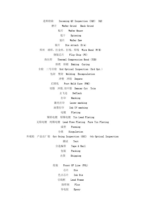
进料检验 Incoming QC Inspection (IQC) IQI磨片 Wafer Grind Back Grind贴片 Wafer Mount甩干 Spinning划片 Wafer Saw装片 Die Attach (D/A)焊丝球焊,打金丝,打线,焊线 Wire Bond (W/B)倒装芯片 Flip Chip (FC)热压焊 Thermal Compression Bond (TCB)烘烤烘箱 Baking Curing全检三号目检 3rd Optical Inspection (3rd Opt.)包封塑封 Molding Encapsulation冲塑冲胶 Degate后固化 Post Mold Cure (PMC)切筋冲筋,切中筋 Damcar Cut Trim去飞边 Deflash打印 Marking激光打印 Laser marking油墨打印 Ink UV marking电镀 Plating锡铅电镀铅锡电镀 Tin Lead Plating无铅电镀纯锡电镀 Lead Free Plating Pure Tin Plating成型 Forming分离 Singulation外观检产品出厂检 Out Going Inspection (OGI) 4th Optical Inspection测试 Test分选编带 Tape & Rail包装 Packing出货 Shipping组装 Front OF Line (FOL)芯片 Die色点芯片 Ink Die引线框 Lead Frame助焊剂 Flux导电胶 Epoxy蓝膜 Blue Tape / Mounting tape 圆片 Wafer金丝 Gold wire推晶 Die shear弧高 Loop Height弧度 Wire Loop布线图 Bond diagram布线错误 Wrong Bonding焊丝拉力测克,拉丝 Wire Pull 推球金球剥离 Ball shear细刀 Capillary扭曲 Bending翘曲 Bow / Warpage硅屑 Silicon Dust沾污 Contaminate压伤 Dented变形 Distort缺角 Chip Die锡膏回流 Solder Reflow银厚度 Silver Thickness毛刺针刺 Burr塌丝 Depress Wire超波膜 UV Tape火山口 Crater Ring断丝 Broken Wire昂球 Lifted Bond飞球 Sky Ball金属剥落 Lifted Metal昂楔 Lifted Wedge高尔夫球 Golf Ball扁球 Flat Ball半球 Insufficient Ball Size 不粘 Non-Stick芯片裂缝 Crack Die 错方向 Wrong Orientation焊不牢 Incomplete Bond无焊 No Bonding翘芯片 Lifted Die误置芯片 Misplaced Die芯片装斜 Tilted Die芯面粘胶 Epoxy On Die导电胶不足 Insufficient Epoxy多胶 Excess Epoxy导电胶气孔 Epoxy Void镀层气孔 Solder Void导电胶裂缝 Epoxy Crack金属划伤 Saw Into Metal擦痕 Scratches墨溅 Ink Splash薄膜气泡 Tape Bubbles边沿芯片 Edge Die镜子芯片 Mirror Die飞片 Fly Die封装 End Of Line (EOL)排气 Air vent托块 Insert刀片 Punch型腔 Cavity料饼塑料,树脂,环氧 Mold Compound Mold pallet基岛 Paddle (PAD) DAP共面性 Coplanity点温计 Digimite空封 Dummy Molded Strip废胶跑料,废料 Mold Flash小脚 Gate Remain脚间距开档,总宽,跨度 Lead Tip to Tip Total Width, Lead Distance.包封偏差 Molding Mismatch包封模具 Mold Chase冲切,成型模具 Dieset清模 Mold Cleaning多肉 Package Bump引线条 Molded Strip溢胶 Mold Bleed包反 Wrong Orientation Molding印偏 Offset Marking焊丝冲弯 Wire Sweep错位 Molding Mismatch偏心 Molding Offset气孔空洞,气泡 Void排气不畅 Air Vent Clog偏脚 Offset Punch注浇口,进浇口 Injection Gate 1st Gate上料框 Frame Loader冲圆 Fan Out模温 Mold Temperature表面粗糙 Rough Surface未填充 Incomplete Mold料饼醒料 Compound Aging顶针 Ejector Pin顶孔顶料孔 Ejector Pin hole定位块 Locator Block粘模 Sticky Mold烘箱 Oven麻点镀层起毛 Solder Blister锡桥搭锡 Solder Bridge镀层起泡拉尖 Solder Bump镀层剥落 Solder Peel Off锡丝 Solder Flick露铜露底材 Expose Copper细脚小脚 Narrow Lead镀层厚度 Plating Thickness变色 (发黄,发黑,发花,水渍,酸斑) Discolor (Yellowish, Blacken, WaterMark)锡球 Solder Pad镀层偏厚或偏薄 Thick or Thin Plating易焊性 Solderability退锡 Solder Remove站立高度 Stand Off切中筋凸出或凹陷 Dambar Protrusion or Intrusion连筋 Uncut Dambar脚长 Lead Length管脚刮伤 Lead Scratches管脚反翘 Lead Tip Bend反切 Wrong Orientation Forming.缺脚缺管,断脚 Missing Lead Broken Lead裂缝胶体破裂 Crack Package微裂缝 Micro Crack崩角缺角,缺损 Chip Package Chip Off成型角度 Foot angle共面性 Coplanarity倒角 Touch Up印章印记 Marking Layout断字 Broken character印记磨糊褪色 Fad Mark打印不良 Illegible Marking打印字间距 Mark Character Distance印记倾斜 Slant Marking漏打 No marking缺字 Missing Character错字 Wrong Marking弄脏 Smear定位针 Location Pin烧氢 Hydrogen Frame扫描打印 Writing laser模板激光 Mask Laser常用的术语集成电路 Integrated Circuit (IC)塞头 Plug托盘 Tray编带, 带盖 Rail, Rail Cover料管 Tube静电袋 Anti Static Bag支持棒 Suspension Bar Fishtail, tie bar 随件单 Traveling Card Run Card去离子水 D.I. Water散热片 Heat Sink品管 Quality Control (QC)品保 Quality Assurance (QA)关卡 QC Gate校验 Calibrate照明放大镜 Dazor Light Ring Light显微镜 Microscope返工 Rework质量标准 Criteria扩散批 Wafer Lot Mother Lot批 Lot抽样 Sample Size (SS)良品 Accept Unit (Acc)不良品 Reject Unit (Rj)良率 Yield次品率不良率 Yield Lost外次率 O.G.I. YieldX管率 X-ray Yield目检 Visual Inspection正面 Top Surface反面 Bottom surface冷藏库料饼存放库 Cold Room Compound storage 表面贴装式 Surface Mount Technology (SMT)报废 Scrap开短路 Open short调机 Machine Buy Off单列直插式 Single Side Lead Insert双列直插式 Dual Side Lead Insert Type 内控 Internal / In-house Control在制品 Work In Progress (WIP)。
汉高 百得熊猫白胶卓效环保型 706B 1 18KG 安全技术说明书

安全技术说明书根据GB/T 16483-2008第 1 页共 7 页百得熊猫白胶卓效环保型706B 1*18KG安全技术说明书编号: 557677V001.2修订: 16.09.2020发布日期: 28.04.2022化学品中文名称: 百得熊猫白胶卓效环保型 706B 1*18KG推荐用途:木工胶制造商/进口商/分销商代表公司汉高粘合剂科技(上海)有限公司中国(上海)自由贸易试验区张衡路928号2B(即1幢)105室201204 中国上海市浦东新区中国电话:+86-21-2891 8000传真:+86-21-2891 5137电子邮件: ***************************生效日期: 16.09.2020应急信息:应急电话:+86 21 2891 8311 (24小时)。
物质或混合物的分类根据GB 13690-2009 (化学品分类和危险性公示通则):危险分类危险类别急性危害水生环境类别 3对水生环境有慢性危害类别 3标签要素根据GB 15258-2009 (化学品安全标签编写规定):危险性说明:H412对水生生物有害并具有长期持续影响。
预防措施:P273避免释放到环境中。
废弃处置:P501在适合的处置和废弃设施内,按照可用的法律法规要求,以及废弃时的产品特性,废弃处置内容物/容器。
成分信息: 混合物 根据GB 13690-2009 公布的有害物质:只有那些根据GB13690-2009分类为有害的物质才被列入该表格。
关于危险性说明(H 词组)代号的全文请参考第16部分“其他信息”。
皮肤接触: 立即脱除污染的或浸湿的衣物。
立即用大量流动水至少清洗10分钟。
必要时寻求医生帮助。
眼睛接触: 立即用大量流动清水冲洗(10分钟),就医。
吸入: 移至新鲜空气处。
保暖,置于安静的场所。
根据需要给氧或作人工呼吸。
向医学专家求助。
食入:漱口,给饮1~2杯水。
禁止催吐。
寻求医生帮助。
有害燃烧产物:一氧化碳。
半导体封装胶水介绍
半导体封装胶水介绍
半导体封装胶水是一种用于半导体封装过程中的关键材料,它在半导体芯片与封装基板之间起着粘合和保护作用。
半导体封装胶水通常是一种环氧树脂或硅胶等材料,具有优异的粘合性、导热性和电绝缘性能。
首先,半导体封装胶水在半导体封装过程中起着粘合的作用。
它能够牢固地将半导体芯片与封装基板粘合在一起,确保芯片不会因为外部振动或温度变化而脱落或移位。
这对于保护芯片内部的微小电路元件至关重要,能够确保芯片的稳定性和可靠性。
其次,半导体封装胶水还具有良好的导热性能。
在半导体工作时会产生大量的热量,如果不能及时地散热,会影响芯片的性能和寿命。
因此,封装胶水需要具有良好的导热性能,能够有效地将热量传导到封装基板上,进而散热到外部环境中。
另外,半导体封装胶水还需要具有良好的电绝缘性能。
在半导体芯片工作时,需要避免不同电路之间的相互干扰,因此封装胶水需要能够有效地隔离不同的电路,确保它们之间不会相互干扰。
总的来说,半导体封装胶水在半导体封装过程中扮演着非常重
要的角色,它不仅能够确保芯片的稳定性和可靠性,还能够提高芯
片的散热性能和电绝缘性能。
随着半导体技术的不断发展,对封装
胶水的要求也越来越高,相信在未来会有更多创新的封装胶水出现,为半导体行业带来更多的发展机遇。
汉高产品之-COB包封材料
20分钟@80°C 60分钟@60°C
10,000~38,000
110
10分钟@80°C 30分钟@60°C
100,000
41Байду номын сангаас
20分钟@150°C
60,000
126
4 - 6小 时@125°C
20,000
125
4-6小时@125°C
50,000
125
4-6小时@125°C
160,000
125
5分钟@140°C
140
77
9
80
75
22
73
19
73
18
72.5
18
75
20
75
41
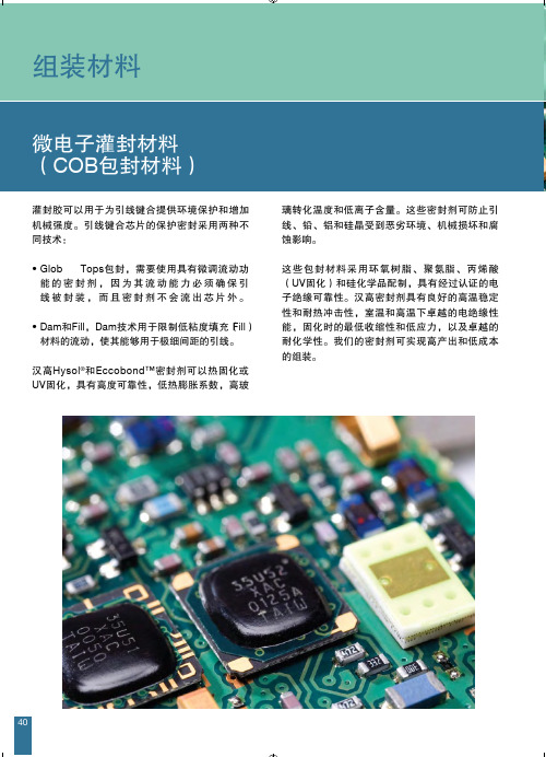
组装材料
微电子灌封材料 (COB包封材料)
COB包封材料 - Glob Tops - UV固化
产品
描述
固化时间
ECCOBOND™ UV9052™
单组分双固化(UV固化和湿固化)粘 合剂,用作含铅密封剂。
在环境温度下,5 秒,使用300W/in
100,000
135
20分钟@150°C
60,000
121
3小时@170°C
220,000
174
HYSOL® FP4460™
高纯度低应力顶部封装半导体密
封剂,比过去的型号具有更高防
2天
潮性能和工作寿命。
3小时@150°C
420,000
171
HYSOL® OT0149-3™
透明顶部封装材料,具有良好的 粘附力,可粘接任何基材。
COB包封材料
Dam
Fill
Glob Tops
UV固化
汉高 ccm 胶黏剂 20116310311594
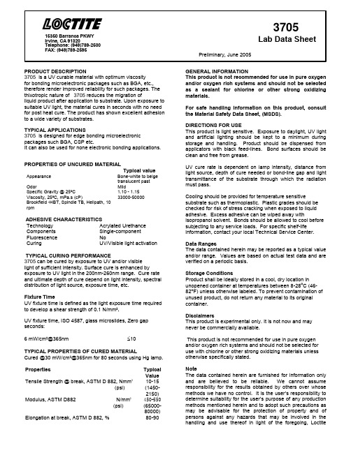
PRODUCT DESCRIPTION3705 is a UV curable material with optimum viscosity for bonding microelectronic packages such as BGA, etc., therefore render improved reliability for such packages. The thixotropic nature of 3705 reduces the migration ofliquid product after application to substrate. Upon exposure to suitable UV light, the material cures in seconds with no need for post heat cure. The product has shown excellent adhesion to a wide variety of substrates.TYPICAL APPLICATIONS3705 is designed for edge bonding microelectronic packages such BGA, CSP etc.It can also be used for none electronic bonding applications.PROPERTIES OF UNCURED MATERIAL Typical value UV cure rate is dependent on lamp intensity, distance from light source, depth of cure needed or bond-line gap and light transmittance of the substrate through which the radiation must pass. Appearance Bone-white to beigetranslucent pastOdor Mild Specific Gravity @ 25ºC 1.10 - 1.15Viscosity, 25ºC, mPa.s (cP) Brookfield -HBT, Spindle TB, Helipath, 10 rpm 33000-50000ADHESIVE CHARACTERISTICS Technology Acrylated Urethance Components Single-component Fluorescence No Curing UV/Visible light activation TYPICAL CURING PERFORMANCE 3705 can be cured by exposure to UV and/or visible light of sufficient intensity. Surface cure is enhanced by exposure to UV light in the 200nm-260nm range. Cure rate and ultimate depth of cure depend on light intensity, spectral distribution of light source, exposure time, etc. Fixture Time UV fixture time is defined as the light exposure time required to develop a shear strength of 0.1 N/mm ². UV fixture time, ISO 4587, glass microslides, Zero gap seconds: 6 mW/cm²@365nm ≤10 TYPICAL PROPERTIES OF CURED MATERIALCured @30 mW/cm²@365nm for 80 seconds using Hg lamp.Properties TypicalValueTensile Strength @ break, ASTM D 882, Nmm ² 10-15(psi) (1450-2150)Modulus, ASTM D882 N/mm ² 450-550(psi) (65000-80000)Elongation at break, ASTM D 882, % 80-90GENERAL INFORMATIONThis product is not recommended for use in pure oxygen and/or oxygen rich systems and should not be selected as a sealant for chlorine or other strong oxidizing materials.For safe handling information on this product, consult the Material Safety Data Sheet, (MSDS).DIRECTIONS FOR USEThis product is light sensitive. Exposure to daylight, UV light and artificial lighting should be kept to a minimum during storage and handling. Product should be dispensed from applicators with black feed-lines. Bond surfaces should beclean and free from grease.Cooling should be provided for temperature sensitive substrate such as thermoplastic. Plastic grades should be checked for risk of stress cracking when exposed to liquid adhesive. Excess adhesive can be wiped away with isopropanol solvent. Bonds should be allowed to cool before subjecting to any service loads. For specific shelf-life information, contact your local Technical Service Center. Data Ranges The data contained herein may be reported as a typical value and/or range. Values are based on actual test data and are verified on a periodic basis. Storage Conditions Product shall be ideally stored in a cool, dry location in unopened container at temperatures between 8-28o C (46-82o F) unless otherwise labeled. To prevent contamination of unused product, do not return any material to its original container. Disclaimers This product is experimental only. It is not now and may never be commercially available. This product is not recommended for use in pure oxygen and/or oxygen rich systems and should not be selected foruse with chlorine or other strong oxidizing materials unless otherwise specifically stated. Note The data contained herein are furnished for information only and are believed to be reliable. We cannot assume responsibility for the results obtained by others over whose methods we have no control. It is the user’s responsibility to determine suitability for the user’s purpose of any production methods mentioned herein and to adopt such precautions as may be advisable for the protection of property and of persons against any hazards that may be involved in the handling and use thereof in light of the foregoing, LoctiteCorporation specifically disclaims all warranties expressed orimplied, including warranties of merchantability or fitness for aparticular purpose, arising from sale or use of LoctiteCorporation’s products. Loctite Corporation specificallydisclaims any liability for consequential or incidental damagesof any kind, including lost profits. The discussion herein ofvarious processes or compositions is not to be interpreted asrepresentation that they are free from domination of patentsowned by others or as a license under any LoctiteCorporation patents that may cover such processes orcompositions. We recommend that each prospective usertest his proposed application before repetitive use, using thisdata as a guide. This product may be covered by one ormore United States or foreign patents or patent applications.Loctite is a Registered Trademark of Loctite Corporation, Hartford, CT 06106。
半导体封装去胶工艺流程
半导体封装去胶工艺流程Semiconductor packaging and encapsulation are crucial processes in the manufacturing of electronic devices. While there are several different methods of packaging and encapsulation, one common technique is the use of a gel-like material to encapsulate the semiconductor chip. This gel acts as a protective barrier, shielding the chip from environmental factors such as moisture, dust, and other contaminants.半导体封装和封装是电子设备制造过程中至关重要的步骤。
虽然有几种不同的封装和封装方法,但一个常见的技术是使用类似凝胶的材料来封装半导体芯片。
这种凝胶起着保护屏障的作用,可以将芯片从湿气、灰尘和其他污染物等环境因素中隔离开来。
The process of gel-based encapsulation involves several steps. First, the semiconductor chip is placed onto a substrate, typically a lead frame, which provides support for the chip. Next, the gel material is dispensed onto the chip and spread out to cover the entire surface. Once the gel is in place, it is cured or solidified to form a protectivelayer around the chip. This encapsulation process is essential for ensuring the reliability and performance of the semiconductor device.基于凝胶的封装过程包括几个步骤。
汉高粘合剂技术创新中心落户上海 助力亚太市场发展
汉高粘合剂技术创新中心落户上海助力亚太市场发展
本刊讯
【期刊名称】《粘接》
【年(卷),期】2016(37)7
【摘要】全球领先的粘合剂、密封剂和功能性涂层解决方案供应商汉高在上海建立全新粘合剂技术创新中心(HAIC)。
这所全新打造的创新中心配备有世界一流的NVH(噪声、振动与声振粗糙度)检测实验室、未来实验室、民用粘合剂实验室及培训中心等,
【总页数】1页(P21-21)
【关键词】技术创新中心;研发资源;密封剂;声振;亚太市场;粗糙度;汽车制造;培训中心;副总裁;柯思
【作者】本刊讯
【作者单位】
【正文语种】中文
【中图分类】TQ432.2
【相关文献】
1.全球最大粘合剂厂汉高集团落户上海 [J],
2.汉高粘合剂技术将助力亚太区软包装市场发展 [J],
3.汉高粘合剂技术第三季度增长稳健亚太市场需求推动业务发展 [J],
4.汉高助力通用设备制造的可持续发展--访汉高粘合剂事业部通用工业大中华区业
务总监Volker Mansfeld [J],
5.汉高黏合剂技术创新中心落户上海,助力亚太市场发展 [J],
因版权原因,仅展示原文概要,查看原文内容请购买。
半导体封装刷胶汉高WBCCapabilityinChina
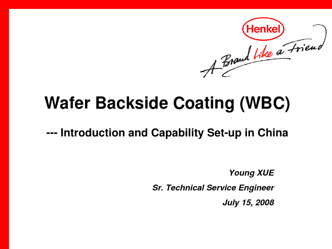
--- IntroductioPnroajnecdt:CTaWpIRa-b7iFliPtyB9S2et-up in China
Tony Winster , Ablestik U.YKo.ung XUE 21 JSurn. Teec2h0n0ic8al Service Engineer
4
XUE Young --- WBC General Introduction and Capability Set-up in China
WBC Merits -
Lead frame standardization
No need for dispensing ; glue is already on 100% of the chip at the desired thickness
8
XUE Young --- WBC General Introduction and Capability Set-up in China
Stencil
For thicker coating (>1mil), it is typically recommended to use open cut stencils. Open cut is big opening in the metal stencil.
Stencil printing
Squeegee
Palette
Vacuum tube
Palette
Stencil printing is mainly wafer backside coating method recommended to customer.
- 1、下载文档前请自行甄别文档内容的完整性,平台不提供额外的编辑、内容补充、找答案等附加服务。
- 2、"仅部分预览"的文档,不可在线预览部分如存在完整性等问题,可反馈申请退款(可完整预览的文档不适用该条件!)。
- 3、如文档侵犯您的权益,请联系客服反馈,我们会尽快为您处理(人工客服工作时间:9:00-18:30)。
Stencil
For thicker coating (>1mil), it is typically recommended to use open cut stencils. Open cut is big opening in the metal stencil.
Stencil Printing Screen Printing Spin Coating
Ablestik has three methods to achieve wafer backside coating process.
7 XUE Young --- WBC General Introduction and Capability Set-WBC General Introduction and Capability Set-up in China
WBC Process Introduction
3
XUE Young --- WBC General Introduction and Capability Set-up in China
WBC Merits -2
Discrete/Small SO Applications
----Eutectic and soft solder is high stress. WBC can improve reliability by reducing cracks ----Eliminate N2 or H2 forming gasses due to lower temperature cure
July 15, 2008
Background
Ablestik introduces a new line of specially designed adhesives that can be applied to the back of a wafer and dried. Conductive and nonconductive wafer backside coating materials have been developed for die sizes 3mm or less and enable such package types as COL, SO, TSOP and QFN. High thermal materials have been developed that are suitable for use in discrete and small power IC devices. The advantages of the wafer backside coating process are: * Bond line thickness and fillet formation can be controlled * Resin bleed is eliminated * Moisture resistance and adhesive strength are improved * WBC materials can achieve higher reliability levels
WBC Training Notes Wafer Backside Coating (WBC)
Project: TWIR-7FPB92 --- Introduction and Capability Set-up in China
Tony Winster , Ablestik U.K. XUE Young 21 June 2008 Service Engineer Sr. Technical
4 XUE Young --- WBC General Introduction and Capability Set-up in China
WBC Merits -1
IC Application
Lead frame standardization
WBC Process
No need for dispensing ; glue is already on 100% of the chip at the desired thickness
Improved reliability regardless of LDF type
L1,260c possible on Ag, Cu, PPF and Aolly42
Improved yields
Reduced die tilt; No bleeding
Improved design flexibility
Tighter die bond to pad ratios; Ability to choose thickness
WBC can offer significant process benefits at least 20-30% cheaper than film.
Paste Process
5 XUE Young --- WBC General Introduction and Capability Set-up in China
Eutectic
----Reduce and standardize backside coating layer
Soft Solder
----Increase line speeds by 2-3 times ----Pb-free die attach solution (Typically soft solder is 95% Pb)
10
XUE Young --- WBC General Introduction and Capability Set-up in China
Squeegee
Squeegee Stencil
Wafer back side material wafer
Metal Shim
Roll bar squeegee (or metal squeegee with reinforced rod at the edge) is recommend to reduce the scooping during printing with big opening stencils. Roll bar squeegee is not recommended for screen printing. Rubber squeegees or metal blade are recommended for screen printing.
Stencil printing
Squeegee
Palette
Vacuum tube
Palette
Stencil printing is mainly wafer backside coating method recommended to customer. Stencil printing is able to provide smooth surface (good performance in roughness) and has good thickness control. Moreover, its process is stable and easy to control. Stencil printing has a strict request to shim and stencil thickness uniformity. In addition, the flatness of palette and squeegee are key factors for printing performance.
12
XUE Young --- WBC General Introduction and Capability Set-up in China
Palette
Squeegee
Palette
Vacuum tube
Palette
Printing back side coating on wafers requires vacuum chuck to make the wafer stable. Palette needs to be very smooth and flat so as not to damage the front face of the wafer. Besides, the flatness of palette will cause print thickness variation. Granite palette usually shows better performance than metal palette. But its weight is really high and it may cause negative effect on printer.
WBC can be dropped into existing soft solder and eutectic lines.
6 XUE Young --- WBC General Introduction and Capability Set-up in China
WBC Wafer Back Side Coating
Metal Opening
Frame
Stencil opening can selected based on the print area requirements. Typically opening will be 2 mm less than the wafer diameter. (Example: 198 mm opening for 200 mm wafer). Stencil thickness depends on the coating thickness requirement. For thinner coating (≤1 mil), screens are recommended.