高精度的数字电位器X9C103
X9C102系列数字电位器

DESCRIPTIONThe Xicor X9C102/103/104/503 is a solid state nonvola-tile potentiometer and is ideal for digitally controlledresistance trimming.The X9C102/103/104/503 is a resistor array composed of 99 resistive elements. Between each element and at either end are tap points accessible to the wiper element.The position of the wiper element is controlled by the CS ,U/D , and INC inputs. The position of the wiper can be stored in nonvolatile memory and then be recalled upon a subsequent power-up operation.The resolution of the X9C102/103/104/503 is equal to the maximum resistance value divided by 99. As an example, for the X9C503 (50K Ω) each tap point repre-sents 505Ω.All Xicor nonvolatile memories are designed and tested for applications requiring extended endurance and data retention.FEATURES•Compatible with X9102/103/104/503•Low Power CMOS —V CC = 5V—Active Current, 3mA Max —Standby Current, 500µA Max •99 Resistive Elements—Temperature Compensated—± 20% End to End Resistance Range •100 Wiper Tap Points—Wiper Positioned via Three-Wire Interface —Similar to TTL Up/Down Counter —Wiper Position Stored in Nonvolatile Memory and Recalled on Power-Up•100 Year Wiper Position Data Retention •X9C102 = 1K Ω•X9C103 = 10K Ω•X9C503 = 50K Ω•X9C104 = 100K ΩE 2POT ™ Nonvolatile Digital PotentiometerX9C102/103/104/503E 2POT ™ is a trademark of Xicor, Inc.3863 FHD F01FUNCTIONAL DIAGRAML WHVX9C102/103/104/503PIN DESCRIPTIONSV H and V LThe high (V H) and low (V L) terminals of the X9C102/103/ 104/503 are equivalent to the fixed terminals of a mechanical potentiometer. The minimum voltage is –5V and the maximum is +5V. It should be noted that the terminology of V L and V H references the relative position of the terminal in relation to wiper movement direction selected by the U/D input and not the voltage potential on the terminal.V WV W is the wiper terminal, equivalent to the movable terminal of a mechanical potentiometer. The position of the wiper within the array is determined by the control inputs. The wiper terminal series resistance is typically 40Ω.Up/Down (U/D)The U/D input controls the direction of the wiper movement and whether the counter is incremented or decremented.Increment (INC)The INC input is negative-edge triggered. Toggling INC will move the wiper and either increment or decrement the counter in the direction indicated by the logic level on the U/D input.Chip Select (CS)The device is selected when the CS input is LOW. The current counter value is stored in nonvolatile memory when CS is returned HIGH while the INC input is also HIGH. After the store operation is complete the X9C102/ 103/104/503 will be placed in the low power standby mode until the device is selected once again.PIN CONFIGURATIONPIN NAMESSymbol DescriptionV H High TerminalV W Wiper TerminalV L Low TerminalV SS GroundV CC Supply VoltageU/D Up/Down InputINC Increment InputCS Chip Select InputNC No Connect3863 PGM T01V CCCSV LV W3863 FHD F02.2INCU/DV HV SS12348765X9C102/103/104/503DIP/SOICX9C102/103/104/503DEVICE OPERATIONThere are three sections of the X9C102/103/104/503: the input control, counter and decode section; the non-volatile memory; and the resistor array. The input control section operates just like an up/down counter. The output of this counter is decoded to turn on a single electronic switch connecting a point on the resistor array to the wiper output. Under the proper conditions the contents of the counter can be stored in nonvolatile memory and retained for future use. The resistor array is comprised of 99 individual resistors connected in series. At either end of the array and between each resistor is an electronic switch that transfers the potential at that point to the wiper.The INC, U/D and CS inputs control the movement of the wiper along the resistor array. With CS set LOW the X9C102/103/104/503 is selected and enabled to respond to the U/D and INC inputs. HIGH to LOW transitions on INC will increment or decrement (depending on the state of the U/D input) a seven-bit counter. The output of this counter is decoded to select one of one-hundred wiper positions along the resistive array.The wiper, when at either fixed terminal, acts like its mechanical equivalent and does not move beyond the last position. That is, the counter does not wrap around when clocked to either extreme.The value of the counter is stored in nonvolatile memory whenever CS transistions HIGH while the INC input is also HIGH.When the X9C102/103/104/503 is powered-down, the last counter position stored will be maintained in the nonvolatile memory. When power is restored, the con-tents of the memory are recalled and the counter is reset to the value last stored.OPERATION NOTESThe system may select the X9C102/103/104/503, move the wiper, and deselect the device without having to store the latest wiper, position in nonvolatile memory. The wiper movement is performed as described above; once the new position is reached, the system would the keep INC LOW while taking CS HIGH. The new wiper position would be maintained until changed by the system or until a power-down/up cycle recalled the previously stored data.This would allow the system to always power-up to a preset value stored in nonvolatile memory; then during system operation minor adjustments could be made. The adjustments might be based on user preference: system parameter changes due to temperature drift, etc...The state of U/D may be changed while CS remains LOW. This allows the host system to enable the X9C102/103/104/503 and then move the wiper up and down until the proper trim is attained.T IW/R TOTALThe electronic switches on the X9C102/103/104/503 operate in a “make before break” mode when the wiper changes tap positions. If the wiper is moved several positions, multiple taps are connected to the wiper for t IW (INC to V W change). The R TOTAL value for the device can temporarily be reduced by a significant amount if the wiper is moved several positions.R TOTAL with V CC RemovedThe end to end resistance of the array will fluctuate once V CC is removed.SYMBOL TABLEX9C102/103/104/503ABSOLUTE MAXIMUM RATINGS*Temperature under Bias..................–65°C to +135°C Storage Temperature.......................–65°C to +150°C Voltage on CS, INC, U/D and V CCwith Respect to V SS...............................–1V to +7V Voltage on V H and V LReferenced to V SS.................................–8V to +8V ∆V = |V H–V L|X9C102 (4V)X9C103, X9C503, and X9C104 (10V)Lead Temperature (Soldering, 10 seconds)....+300°C Wiper Current.....................................................±1mA *COMMENTStresses above those listed under “Absolute Maximum Ratings” may cause permanent damage to the device. This is a stress rating only and the functional operation of the device at these or any other conditions above those listed in the operational sections of this specifica-tion is not implied. Exposure to absolute maximum rating conditions for extended periods may affect device reliability.ANALOG CHARACTERISTICSElectrical CharacteristicsEnd-to-End Resistance Tolerance (20)Power Rating at 25°CX9C102.......................................................16mW X9C103, X9C503, and X9C104..................10mW Wiper Current............................................±1mA Max. Typical Wiper Resistance.........................40Ω at 1mA Typical Noise..........................< –120dB/Hz Ref: 1VResolution Resistance.............................................................1%LinearityAbsolute Linearity(1)........................................±1.0 Ml(2) Relative Linearity(3).....................................±0.2 Ml(2)Temperature Coefficient(–40°C to +85°C)X9C102......................................+600 ppm/°C Typical X9C103, X9C503, X9C104........+300 ppm/°C Typical Ratiometric Temperature Coefficient............±20 ppm Wiper AdjustabilityUnlimited Wiper Adjustment (Non-Store operation) Wiper Position Store Operations...................10,000 Data Changes Physical CharacteristicsMarking IncludesManufacturer‘s TrademarkResistance Value or CodeDate CodeTest Circuit #1Test Circuit #2Notes:(1)Absolute Linearity is utilized to determine actual wiper voltage versus expected voltage= (V w(n)(actual) – V w(n)(expected)) = ±1 Ml Maximum.(2) 1 Ml = Minimum Increment = R TOT/99.(3)Relative Linearity is a measure of the error in step size between taps = V W(n+1) – [V w(n) + Ml] = +0.2 Ml.X9C102/103/104/503 RECOMMENDED OPERATING CONDITIONSTemperature Min.Max. Commercial0°C+70°C Industrial–40°C+85°C Military–55°C+125°C3863 PGM T03.1Supply Voltage Limits X9C102/103/104/5035V ±10%D.C. OPERATING CHARACTERISTICS (Over recommended operating conditions unless otherwise specified.)LimitsSymbol Parameter Min.Typ.(4)Max.Units Test ConditionsI CC V CC Active Current13mA CS = V IL, U/D = V IL or V IH andINC = 0.4V to 2.4V @ max. t CYCI SB Standby Supply Current200500µA CS = V CC – 0.3V, U/D and INC =V SS or V CC – 0.3VI LI CS, INC, U/D Input±10µA V IN = V SS to V CCLeakage CurrentV IH CS, INC, U/D Input2V CC + 1VHIGH VoltageV IL CS, INC, U/D Input–10.8VLOW VoltageR W Wiper Resistence40100ΩMax. Wiper Current ±1mAV H VH Terminal Voltage–5+5VV L VL Terminal Voltage–5+5VC IN(5)CS, INC, U/D Input10pF V CC = 5V, V IN = V SS,Capacitance T A = 25°C, f = 1MHz3863 PGM T05.3 STANDARD PARTSPart Number Maximum Resistance Wiper Increments Minimum Resistance X9C1021KΩ10.1Ω40ΩX9C10310KΩ101Ω40ΩX9C50350KΩ505Ω40ΩX9C104100KΩ1010Ω40Ω3863 PGM T08.1 Notes:(4)Typical values are for T A = 25°C and nominal supply voltage.(5)This parameter is periodically sampled and not 100% tested.3863 PGM T04.2X9C102/103/104/503MODE SELECTIONA.C. CONDITIONS OF TESTNotes:(6)Typical values are for T A = 25°C and nominal supply voltage.(7)This parameter is periodically sampled and not 100% tested.(8)MI in the A.C. timing diagram refers to the minimum incremental change in the V W output due to a change in the wiper position.X9C102/103/104/503Typical Frequency Response for X9C102TEST CONDITIONS V CC = 5VTemp. = 25°C Wiper @ Tap 50V H = 0.5V RMSNormalized (0dB @ 1KHz)Test Circuit #1TEST CONDITIONS V CC = 5VTemp. = 25°C Wiper @ Tap 50V H = 2V RMS Test Circuit #1Typical Total Harmonic Distortion for X9C102N O R M A L I Z E D G A I N (d B )9630–3–6–9–12–15–18–210.010.101.0010.00100.001000.0010000.00FREQUENCY IN KHzT H D (%)2.01.81.61.41.21.00.80.60.40.20.00.010.101.0010.00100.001000.0010000.00FREQUENCY IN KHz3863 FHD F063863 FHD F07X9C102/103/104/503Typical Linearity for X9C102Typical Frequency Response for X9C103TEST CONDITIONS V CC = 5VTemp. = 25°C Wiper @ Tap 50V H = 0.5V RMSNormalized (0dB @ 1KHz)Test Circuit #1N O R M A L I Z E D G A I N (d B )9630–3–6–9–12–15–18–210.010.101.0010.00100.001000.00FREQUENCY IN KHz3863 FHD F09X9C102/103/104/503Typical Total Harmonic Distortion for X9C103Typical Linearity for X9C103TEST CONDITIONS V CC = 5VTemp. = 25°C Wiper @ Tap 50V H = 2V RMS Test Circuit #1T H D (%)2.01.81.61.41.21.00.80.60.40.20.00.010.101.0010.00100.001000.00FREQUENCY IN KHz3863 FHD F10X9C102/103/104/503Typical Frequency Response for X9C503Typical Total Harmonic Distortion for X9C503TEST CONDITIONS V CC = 5VTemp. = 25°C Wiper @ Tap 50V H = 2V RMS Test Circuit #1TEST CONDITIONS V CC = 5VTemp. = 25°C Wiper @ Tap 50V H = 0.5V RMSNormalized (0dB @ 1 KHz)Test Circuit #19630-3-6-9-12-15-18-210.010.101.0010.00100.00FREQUENCY IN KHzN O R M A L I Z E D G A I N (d B )1000.0091.81.61.41.21.00.80.60.40.20.00.010.101.0010.00100.00FREQUENCY IN KHzT H D (%)1000.003863 FHD F123863 FHD F13X9C102/103/104/503Typical Linearity for X9C503Typical Frequency Response for X9C104TEST CONDITIONS V CC = 5VTemp. = 25°C Wiper @ Tap 50V H = 0.5V RMSNormalized (0dB @ 1 KHz)Test Circuit #19630-3-6-9-12-15-18-210.010.101.0010.00100.001000.00FREQUENCY IN KHzN O R M A L I Z E D G A I N (d B )3863 FHD F15X9C102/103/104/503Typical Total Harmonic Distortion for X9C104Typical Linearity for X9C104TEST CONDITIONS V CC = 5VTemp. = 25°C Wiper @ Tap 50V H = 2V RMS Test Circuit #12.01.81.61.41.21.00.80.60.40.20.00.010.101.0010.00100.0010000.00FREQUENCY IN KHzT H D (%)1000.003863 FHD F16X9C102/103/104/5033926 FHD F01TYP NOTE: ALL DIMENSIONS IN INCHES (IN PARENTHESES IN MILLIMETERS)MAX.PACKAGING INFORMATION8-LEAD PLASTIC DUAL IN-LINE PACKAGE TYPE PNOTE: ALL DIMENSIONS IN INCHES (IN PARENTHESES IN MILLIMETERS)X9C102/103/104/503PACKAGING INFORMATION8-LEAD PLASTIC SMALL OUTLINE GULL WING PACKAGE TYPE SNOTE: ALL DIMENSIONS IN INCHES (IN PARENTHESIS IN MILLIMETERS)3926 FHD F22X9C102/103/104/503ORDERING INFORMATIONX9CXXX X XTemperature RangeBlank = Commercial = 0°C to +70°CI = Industrial = –40°C to +85°CM = Military = –55°C to +125°CPackageP = 8-Lead Plastic DIPS = 8-Lead SOICEnd to End Resistance102 = 1KΩ103 = 10KΩ503 = 50KΩ104 = 100KΩLIMITED WARRANTYDevices sold by Xicor, Inc. are covered by the warranty and patent indemnification provisions appearing in its Terms of Sale only. Xicor, Inc. makes no warranty, express, statutory, implied, or by description regarding the information set forth herein or regarding the freedom of the described devices from patent infringement. Xicor, Inc. makes no warranty of merchantability or fitness for any purpose. Xicor, Inc. reserves the right to discontinue production and change specifications and prices at any time and without notice.Xicor, Inc. assumes no responsibility for the use of any circuitry other than circuitry embodied in a Xicor, Inc. product. No other circuits, patents, licenses are implied.U.S. PATENTSXicor products are covered by one or more of the following U.S. Patents: 4,263,664; 4,274,012; 4,300,212; 4,314,265; 4,326,134; 4,393,481; 4,404,475;4,450,402; 4,486,769; 4,488,060; 4,520,461; 4,533,846; 4,599,706; 4,617,652; 4,668,932; 4,752,912; 4,829, 482; 4,874, 967; 4,883, 976. Foreign patents and additional patents pending.LIFE RELATED POLICYIn situations where semiconductor component failure may endanger life, system designers using this product should design the system with appropriate error detection and correction, redundancy and back-up features to prevent such an occurence.Xicor's products are not authorized for use in critical components in life support devices or systems.1.Life support devices or systems are devices or systems which, (a) are intended for surgical implant into the body, or (b) support or sustain life, and whosefailure to perform, when properly used in accordance with instructions for use provided in the labeling, can be reasonably expected to result in a significant injury to the user.2.A critical component is any component of a life support device or system whose failure to perform can be reasonably expected to cause the failure of the lifesupport device or system, or to affect its safety or effectiveness.。
可燃气体数字显示探头设计
可燃气体数字显示探头设计作者:张立国, 佟仕忠, 付贵增, 马书闻来源:《现代电子技术》2010年第17期摘要:设计一种可燃气体数字显示探头,介绍了数字显示探头的工作原理及其软、硬件的设计。
显示探头的探测器由TGS842半导体金属氧化物可燃气体传感器构成,配以OP07放大器对检测信号进行放大,利用高精度的数字电位器根据不同环境对零点、量程做相应的调整,并用TLC549实现A/D转换把数字信号传送给AT89C51微控器,从而实现可燃气体浓度的实时显示和声光报警。
再由XTR105芯片把标准的4~20 mA电流信号传送给中央控制系统,同时用软件对信号进行滤波、报警处理。
关键词:检测电桥; 霍尔元件; 电源模块; 报警处理中图分类号:TN710-34文献标识码:A文章编号:1004-373X(2010)17-0160-04Design of Digital Display Probe for Combustible GasZHANG Li-guo, TONG Shi-zhong, FU Gui-zeng, MA Shu-wen(School of Control and Information Engineering, Liaoning Shihua University, Fushun 113001, China)Abstract: A kind of combustible gas digital display probe is designed. The working principle and software & hardware design of the digital display probe are introduced. The detector of the probe is composed of TGS842 semiconductor metallic oxide combustible gas sensor, coupled with OP07 amplifier to amplify the detected signal. The high- d to adjust the measuring range and zero. The TLC549 is employed to achieve A / D convertion and transmit the digital signal to the AT89C51 microcontroller to implement the real-time display and sound and light alarm of combustible gas concentration, and then transmit the standard 4~20 mA current signal to the central control system by the XTR105 chips. At the same time, the signal is filtered and alarm is processed with the software.Keywords: detection bridge; Hall element; power supply module; alarm handling收稿日期:2010-03-30可燃气体测量仪器是一种广泛用于石油化工、天然气、矿井、冶金、油库等众多易燃易爆场所的检测设备。
全国大学生电子设计竞赛信号调理电路

◦ 一般会比电源电压窄1V~几V ◦ 输入轨到轨运放(Rail-to-rail input,RRI),输入可接 近电源电压,或略超过电源电压(0.1V一般)
共模抑制比(Common-mode rejection ratio, CMRR):差模电压增益与共模电压增益的比值, 用dB表示
Av趋近于∞ Ri趋近于∞ Ro趋近于0 虚短:v+=v虚断:i+=i-=0
分析运放常用的条件
反相放大器
类型:电压并联负反馈
因 v v 则 v 0 则 i1 if 因 i 0 由图
v v vs i1 s R1 R1
vs+ -
if
Rf
i1
精密运放 高速运放 差分放大 仪表放大器 电流反馈型运算放大器(CFB) 比较器
R2 (V 2 V 1) R1 适用于正负噪音相当的场合 Vout
AD8276
三运放搭建仪表放大器原理图 =两个同相放大器+一个增益固定(为1)的差分放 大器 集成仪表放大器:INA128(TI)、AD521、 AD620 仅需添加少量的电阻,即可实现
◦ AD602、AD603 ◦ VCA810、VCA822等
利用VGA实现AGC功能
◦ 通信接收机中的应用
避免自激
直流特性差、适合放大高频交流信号、带宽不因频 率增加而减小、反馈电阻需恒定(一般比较小,参 照datasheet) Rf决定-3db带宽,稳定性受Rf影响 压摆率高,几千V/us 常用型号:OPA695(1400MHz、4300V/us)、 AD8009(700MHz、5500V/us)等 选仪器仪表、放大器类题的同学注意此类运放,一 些使用方法和常规运放不一样
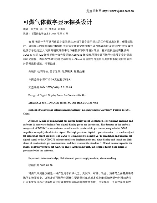
常用芯片的型号、性能指标和适用场合
AD620
温度传感器
DS18B20
8.00
GPS模块
GSR-210
400.00
时钟芯片
DS1302
4.00
混频器
NE602
收音机芯片
LA1260
收音机芯片
CXA1019
收音机芯片
CXA1238
收音机芯片
TDA8127
接收芯片
MC3362
8.20
接收芯片
MC3363
接收芯片
MC3357
18.00
X9C102
6
9.50
1kΩ,32级
数字电位器
X9C102/103
6
9.50
10 kΩ,32级
数字电位器
X9C503
6
9.50
50 kΩ,32级
数字电位器
X9C104
6
9.50
100 kΩ,32级
数字电位器
MAX5161
200kΩ、32级
PLL
NE567
2.80
PLL
MC145151-2
38.00
并行码输入可编程PLL
PGA202
±6~±18V
14
1
1-1000
250kHz
65.00
PGA204
65.00
程控增益放大器
PGA203
±6~±18V
14
1
1-8
250k
无
比较器
LM339
单电源2~36
双电源±1V~±18V
14
4
0.70
比较器
LM393
单电源2V~36V
8
2
双控制器矿井低压电网馈电保护装置

双控制器矿井低压电网馈电保护装置摘要:针对我国矿井工程供电系统的特点,设计一种将交流采集、故障检测与控制相分离的新型馈电开关智能控制器,解决了现有馈电装置响应速度慢等缺点;采用附加直流和零序电压与零序电流相位相结合的方法,较好的解决了现有馈电开关选择性漏电检测可靠性、稳定性差的问题。
添加rs485和can工业通信总线,方便各个系统之间通讯与连接。
我国煤矿井下低压电网多为三相中性点不接地供电系统,该供电系统对选择性漏电保护要求较高,因此可靠稳定的馈电智能开关是矿井安全所必须的。
文章设计一种采用附加直流和零序电压与零序电流相位相结合的选择性漏电检测判别方法,该方法在硬件和软件方面均采取了多重选择性漏电判别规则,大大提升了馈电开关检测稳定性。
该馈电开关兼有rs485和can 工业通信总线,方便各种系统之间相互兼容和数据共享。
关键词:馈电开关;avr;漏电检测1 引言我国是一个产煤大国,由于矿井内部设备庞杂,其运转需要消耗大量电能,其供电设施的稳定与否,对整个矿井安全工作、高效生产有着直接影响。
馈电开关控制器主要用于矿井供电设备的故障检测与电源控制。
在具有短路保护、过流保护、过载保护、等传统故障检测功能的同时,还具有可调式漏电保护功能。
目前矿井所使用的馈电开关大多采用单芯片的系统结构,该系统中央处理芯片不仅需要采集电网中各项参数,还需对测量参数进行处理与检测。
延长设备响应时间,增加了矿井的运行的危险系数。
为解决该类问题,本系统采用双芯片结构,将系统分为交流信号采集模块与信号处理模块。
交流信号采集模块采用电网计量芯片作为主控核心,主要负责电网中输入信号参数测量,故障检测与处理模块选用单片机作为其主控核心,主要负责数据处理与故障检测等功能有效地提高故障响应速度。
2 矿井低压电网漏电特征及选择性漏电保护原理我国矿井井下低压电网供电系统基本采用中性点不接地方式,其漏电电流分布特点如图1所示。
该图所示煤矿电网模型主要由低压辐射式电网为主,该电网模型采用三线供电结构,l1、l2、l3分别代表电网结构中三条支路,在各个支路的测量节点上分别安装zt1、zt2、zt3三个零序电流互感器。
全国电子设计大赛射频宽带放大器

全国电子设计大赛射频宽带放大器(D题)摘要本设计以增益调整、带宽预置、单片机反馈调节为核心,制作一个射频宽带放大器,要求具有0.3~100MHz通频带,增益0~60dB范围内可调,并且实现输入输出阻抗、最大输出正弦波有效值、指定频带内平坦度等功能指标要求。
由于系统输入信号小,频率高,带宽要求大,可控增益范围宽,并且需要满足平坦度、输出噪声电压等指标。
为此,采用高增益带宽运放组成频带预置、AD8367的压控增益放大系统完成增益调整、单片机实现反馈调节。
除此之外,通过增加缓冲级、外加硬件保护措施有效地抑制了高频信号的噪声和自激振荡。
经测试,系统对mV≤的输入信号实现了增益0~60dB范围内可调,带宽0.3~100MHz,并在11~80MHz频带内增益起伏dB1≤,且全程波形无明显失真。
完成了题目所要求的所有基本要求以及绝大部分发挥部分的性能指标。
关键字:带宽预置AD8367压控增益单片机1. 系统方案设计与论证1.1总体方案设计与论证分析该射频宽带放大器设计的指标,为达到题目所设定带宽与增益可调,并且能够满足在输入和输出阻抗=50Ω的情况下,最大输出正弦波电压有效值达到要求的目的,我们将整个系统分为前置缓冲级、带宽预置、增益调整、输出缓冲级、峰值检波等部分组成,主控器采用STC12系列单片机。
系统整体框图如图1所示: 图1 系统框图1.2前置缓冲级的方案论证与选择前置缓冲电路使用电压跟随器实现,如图2所示。
考虑到本系统的通频带为0.3~100MHz ,且输入阻抗限定为50Ω,由正相输入电压跟随器的输入阻抗为R j 趋于无穷大,所以图2电路的输入阻抗为k k k k R R R R R R R R ≈+*==j jj n i //。
则可令实际电路取R k =50Ω以达到输入阻抗要求。
除此之外,此前置放大电路还具有缓冲、避图2 前置缓冲级免引入噪声等作用,起到了良好的隔离功能。
其电压增益接近于1,运算放大器选用AD8005,此放大器的增益带宽积达到270MHz 。
基于MSP430的X9C102、103、103、503等数字电位器的驱动程序
BCSCTL2|=SELM1+SELS; //MCLK为8MHZ,SMCLK为8MHZ
do
{
IFG1&=~OFIFG; //清除震荡标志
for(i=0;i<100;i++)
_NOP(); //延时等待
void SYS_Init();
****************************************x9.c************************************
#include "initial.h"
#include "X9.h"
/******************************************************************************
函数名称:X9_Init()
函数功能:数控电位器初始化,包括对其复位,具体见函数体。
函数参数:无
函数返回值:无
******************************************************************************/
void X9_Init()
****************************************main.c************************************
#include "initial.h"
#include "X9.h"
void main()
{
SYS_Init();
文氏电桥陷波的原理
2 文氏电桥陷波的原理由文氏电桥组成的基波抑制电路(陷波器)如图l所示。
电桥的元件参数关系为Rl=2R2,C1=C2=C,R3=R4=R此时,电桥的抑制频率为因为Rl=2R2,对任一频率信号,UAD=Ui/3。
由计算可知:当输入信号频率f=fo 时,UBD=Ui/3,则UAB=0。
此时,电桥处于平衡状态,输出为O。
当输入信号频率f偏离fo时,电桥失去平衡,则有电压输出。
文氏电桥无源滤波器电路的选择特性很差。
实际工作中,需要阻带很窄、选择性很强的陷波器,为此采用文氏电桥组成的有源陷波电路,如图2所示。
此时陷波的频率为l kHz。
Al、A2是电压跟随器组态,均有缓冲隔离作用,具有高输入阻抗和低输出阻抗特性,对选频电路的谐振频率无影响,A1输出的部分电压反馈至A2的同相端,并经A2输出到电桥桥臂。
调节Rp可调节反馈量,从而改变Q值,以达到锐通带选频作用。
若不加正反馈,在l kHz附近二次谐波的特性曲线就会下降,不能进行准确测量。
如果反馈量与频率特性有关,用可变电阻器Rp调整;如果衰减特性已调准,Q值已选定,则Rp可换成固定电阻器。
在Al的反馈回路中加入电阻器R8是为了抵消输入偏流,以减小直流漂移。
C3的作用是抑制尖峰脉冲。
当f=fo时,电桥平衡,Al的输出为0;f偏离fo时,电桥失衡,有输出电压。
因此该电路能抑制基波,使谐波通过。
若取fo=l kHz,C=0.01μF,由R=l/2πfoC来计算R,求得R=15 kΩ。
A1、A2均为集成运算放大器,可选NE5532A型。
高Q值的陷波器选择性好。
但中心频率fo易偏移,会引起较大的测量误差,因此,测量失真度时可采用二级甚至三级串联调谐设计,使之具有中心频率为±1%的衰减带宽。
3 系统模块智能化数控调谐文氏电桥陷波器包括陷波频率调谐文氏电桥、有效值检波器、A/D采样电路和单片机控制电路,如图3所示。
在系统中,一个未知频率的信号输入文氏电桥之后,在某一个频率点进行陷波,通过有效值检波电路对文氏电桥输出的残余信号进行有效值检波;A/D采样电路对检波后产生的直流电压进行采样,转换成数字信号,并且将数据传输到单片机;单片机对此数据进行判断,当采集到的直流电平为最小值时,文氏电桥的谐振中心频率正好是所需的陷波频率(即最接近基频);如果采集到的直流电平不是最小值,那么单片机将控制改变文氏电桥的电阻和电容,使其中心频率接近基频。
程控放大器设计的方法总结与分析
程控放大器设计的方法总结与分析作者:江朝晖李想陆元洲单桂朋来源:《高教学刊》2016年第20期摘要:程控放大器广泛应用于数据采集系统和自动化仪表。
程控放大器设计是电子系统设计课程的重点和难点内容之一。
文章归纳了五种程控放大器设计方案,比较了各自的特点,并分析了放大器设计中增益与带宽关系。
本研究有助于电子信息工程专业学生对相关课程内容的理解,提高在综合实践、毕业设计、电子设计竞赛和应用开发中的创新能力。
关键词:程控放大器;设计方法;增益带宽积;总结与分析中图分类号:G642 文献标志码:A 文章编号:2096-000X(2016)20-0062-03Abstract: Program-controlled amplifier is widely used in data acquisition system and automatic instrument. The design of program-controlled amplifier is one of the key and difficult points in the course of electronic system design. In this paper, five kinds of design proposals were summarized,their features were compared and the relationship between gain and bandwidth of amplifier was analyzed. This research is helpful to the understanding of the relevant course content for students majored in electronic information engineering, and can improve the innovation ability in the comprehensive practice, graduation design, electronic design competition and application development.Keywords: program-controlled amplifier; design method; gain bandwidth product;summary and analysis引言放大电路是模拟信号采集的核心环节,基于集成运放的放大电路设计与应用是当前技术的主流。
基于电子快门自动增益的CCD驱动电路研究
基于电子快门自动增益的CCD驱动电路研究翟晶晶【摘要】为了满足目前CCD测量领域中高速、高精度的测量要求,设计了TCD1304传感器的专用驱动电路.该驱动电路的一大特性就是电子快门,其将光积分时间缩短了一个数量级,至几个微秒,极大地提高了测量速度;同时,通过对CCD输出信号A/D采样分析,实时调节电子快门时间,实现自动调节控制,提高了测量精度.经实验证明,该测量方法在高速实时在线测量领域有很好的应用前景.【期刊名称】《现代电子技术》【年(卷),期】2010(033)019【总页数】3页(P188-190)【关键词】电子快门;自动增益;TCD1304;CCD传感器【作者】翟晶晶【作者单位】中国船舶重工集团公司,第七一〇研究所,湖北,宜昌,443003【正文语种】中文【中图分类】TN919-340 引言CCD是以电荷包的形式存贮和传递信息的半导体表面器件,目前市场上的CCD器件并未对其驱动信号、输出信号做任何处理。
因此,在实际应用中,需要根据CCD的型号、用途和应用领域的不同而设计不同的驱动电路,以及数据采集、处理系统[1]。
CCD的光积分时间决定着CCD的曝光量,在不同的光照强度下,需要的实际光积分时间不同。
光强较弱时需要较长的光积分时间,以使光敏单元吸收到足够的光信息;相反,光强很强时,光积分时间不能太长,否则CCD的输出信号会饱和失真,不能准确地反应要测量的信息。
因此要得到精确的测量信号,就需要实时的调节光积分时间。
CCD传感器必须在一定的驱动脉冲的作用下才可以完成信号电荷的转移、输出。
在一定的驱动频率内,提高驱动信号的频率则会加快电荷包的移动,从而提高测量速度;反之,降低驱动信号的频率则会降低测量速度。
因此要提高测量速度就要提高驱动信号的频率,而在某些场合需要将光积分时间提高到10 μs时,就需要将时钟频率提高到几百兆,频率太高又引出更难、更复杂的问题,而且这种方法下测量速度的提高空间也是有限的。