基于单片机数字电压表电路设计外文文献原稿和译文
基于单片机的新型数字式电压表设计

多个并行输出口, 用 于 串/并 转 换 , 驱 动 CD4511 锁 存- 译 码 器 进 行 LED 数码管显示。数据从单片机输出 经 74LS04 反相器进入 74LS164 的 输 入 端 , 而 时 钟 脉 冲 经 74LS04 反 相 器 连 接 到 74LS164 的 CLK 脉冲信号端, 在 LED 显示相应的十 进制数字, 从而完成电压有效值的显示。
中 文 核 心 期 刊 《 微 计 算 机 信 息 》( 嵌 入 式 与 S OC )2008 年 第 24 卷 第 3-2 期
(224002 江苏盐城 盐城师范学院 信息科学与技术学院)李永 (Depar tment of Computer Science and Technology, Yanchang Teacher ’s College, J iangsu Yancheng 224002)Li Yong 通 讯 地 址:(224002 江 苏 省 盐 城 师 范 学 院 信 息 科 学 与 技 术 学 院)李永
高达 40V。
图 3 中, PIN1 为电流源输出端,在 fout 输出逻辑低电平时, 电
路对电容 C2 充电, PIN2 为增益调整, 改 变 R4 的 值 可 调 节 电 路
《P LC 技术应用 200 例》
邮局订阅号: 82-946 360 元 / 年 - 133 -
单片机开发与应用
中 文 核 心 期 刊 《 微 计 算 机 信 息 》( 嵌 入 式 与 S OC )2008 年 第 24 卷 第 3-2 期
息科学技术学院硕士研究生, 主要研究方向:信号与信息处理;
吴学杰:男 , (1964- ), 汉 族 , 研 究 员 , 汉 族 西 南 交 通 大 学 牵 引 动 力
基于单片机下的数字电压表设计毕业论文
河南理工大学万方科技学院本科毕业论文基于单片机下的数字电压表设计毕业论文目录前言 (1)1 设计任务与分析 (3)1.1 设计任务简介及背景 (3)1.1.1 单片机简介 (3)1.1.2 背景及发展情况 (3)1.2 设计任务及要求 (5)1.3 设计总体方案及方案论证 (5)1.4 数据输入模块的方案与分析 (7)1.4.1 芯片选择 (6)1.4.2 实现方法介绍 (6)1.4.3 输入模块流程图 (10)1.5 A/D模块的方案与分析 (10)1.5.1 芯片的选择 (11)1.5.2 实现方法介绍 (11)1.5.3 A/D模块流程图 (13)1.6 数据处理及控制模块 (13)1.6.1 芯片选择 (14)1.6.2 实现方法介绍 (14)1.6.3 数据处理及控制模块流程图 (14)1.7 显示模块 (15)1.7.1 芯片选择 (15)1.7.2 实现方法介绍 (15)2 硬件设计 (16)2.1 数据输入模块原理图 (17)2.2 A/D模块原理图 (18)2.3 控制模块原理图 (20)2.4 显示模块原理图 (21)3 软件设计 (23)3.1 主程序流程图 (23)3.2 子程序介绍 (24)3.2.1 初始化程序 (24)3.2.2 中断子程序 (24)3.2.3 档位选择子程序 (25)4 主要芯片 (29)本科毕业论文4.1 AT89C52的功能简介 (29)4.1.1 AT89C52芯片简介 (29)4.1.2 引脚功能说明 (29)4.2 ICL7135功能简介 (31)4.2.1 ICL7135 芯片简介 (31)4.2.2 引脚功能说明 (32)4.3 LCD1602功能简介 (35)4.3.1 LCD1602芯片简介 (35)4.3.2 引脚功能说明 (35)4.4 CD4052的功能介绍 (38)4.4.1 CD4052芯片简介 (38)4.4.2 引脚功能说明 (39)4.5 CD4024的功能介绍 (39)4.5.1 CD4024芯片简介 (39)4.5.2 引脚功能说明 (40)4.6 OP07的功能介绍 (40)4.6.1 OP07的功能简介 (41)4.6.2 引脚功能说明 (41)结论 (42)致谢 (44)参考文献 (45)河南理工大学万方科技学院本科毕业论文前言数字电压表(Digital Voltmeter)简称DVM,它是采用数字化测量技术,把连续的模拟量转换成不连续、离散的数字形式并加以显示的仪表。
基于单片机的简易数字电压表设计(任务书+论文)
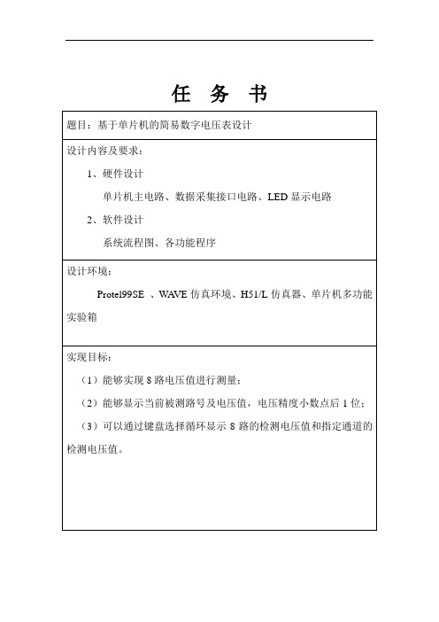
任务书摘要本文介绍了基于89c51单片机的一种8路输入电压测量电路,该电路采用ADC0809作为A/D转换元件,测量范围0至5伏,小数点后显示一位。
要求能够依次显示每路通道电压,而且能够通过拨码开关选择输入通道。
使用3位LED 模块显示,前面一位显示通道号,后面两位显示测量电压值。
本系统主要包括四大模块:数据采集模块、控制模块、显示模块、A/D转换模块。
绘制电路原理图与工作流程图,并进行调试,最终设计完成了该系统的硬件电路。
在软件编程上,采用了汇编语言进行编程,开发环境使用WAVE集成开发环境。
开发了显示模块程序、通道切换程序、A/D转换程序。
关键词:ADC0809;A/D转换;LED显示目录1 方法论证 (5)1.1 系统的设计任务 (5)1.2 设计方案 (5)1.3 软硬件开发环境 (6)2 数字电压表硬件设计 (7)2.1 单片机主电路设计 (7)2.1.1 复位电路 (7)2.1.2 晶振电路 (7)2.2 测量、转换电路设计 (8)2.3 按键电路设计 (9)2.4 显示电路设计 (10)2.4.1 LED数码管构成 (10)2.4.2 显示方式 (11)3 软件设计 (14)3.1 主程序设计 (14)3.1.1 工作流程 (14)3.1.2 存储空间定义安排 (15)3.2 模块程序设计 (15)3.2.1 A/D转换测量程序 (15)3.2.2 显示程序 (16)4 系统调试与分析 (18)4.1 调试内容及问题解决 (18)4.2 系统进一步改进方案 (18)附录1:硬件原理图 (20)附录2:程序清单 (21)参考文献 (24)1 方法论证1.1 系统的设计任务设计单片机主电路、数据采集接口电路、LED显示电路、拨码控制电路,能够实现对8路电压值进行测量,能够显示当前测量通道号及电压值,电压精度小数点后1位,可以通过键盘选择循环显示8路的检测电压值和指定通道的检测电压值。
1.2 设计方案将数据采集接口电路输入电压传入ADC0809数模转换元件,经转换后通过D0至D7与单片机P0口连接,把转换完的模拟信号以数字信号的信号的形式传给单片机,信号经过单片机处理从LED数码显示管显示。
基于AT89C51单片机的数字电压表设计 外文翻译

南京理工大学泰州科技学院毕业设计(论文)外文资料翻译学院(系):电子电气工程学院专业:电气工程及其自动化姓名:干雪燕学号:06020104外文翻译:ROJECTS/TEST/014/INDEX.HTM附件:1.外文资料翻译译文;2.外文原文。
附件1:外文资料翻译译文LED显示屏的数字电压表来源:智能工具包1 引言这是一个很容易建立并且非常准确和有用的数字电压表。
它被设计成一个面板仪表,可用于直流电源供应器或其他需要有一个准确电压指示的地方。
该电路采用的ADC(模拟数字转换器)集成电路CL7107由Intersil公司生产。
该IC采用40引脚的情况下整合了所有必要的电路模拟信号转换为数字,可以直接驱动4个7段LED显示。
在IC中内置的电路是数字转换器,比较器,一个时钟,一个解码器和一个7段LED显示驱动器模拟。
在这里它描述了一个可以显示在0-1999电压范围的直流电压电路。
前面2 LED显示屏数字电压表技术规格 - 特征(1) 电源电压:.............+ / - 5V(对称)。
(2) 电源要求:.............200mA(最大)。
(3) 测量范围:.............+ / - 0-1,999V在四个范围。
(4) 精度:.................0.1%。
(5) 特征:- 小尺寸。
- 简易建筑。
- 成本低。
- 简单的调整。
- 易于读取距离。
- 很少的外部元件。
3 数字电压表的基本原则为了了解电路的运作的原则,说明ADC的集成电路工程是必要的。
该集成电路具有以下非常重要的特点:- 准确性。
- 抗干扰性。
- 无需要一个采样保持电路。
- 它有一个内置的时钟。
- 它不需要精度高的外部元件。
一个模拟数字转换器(ADC),从现在起更好的称为双斜率转换器或集成转换器。
这种类型的转换器通常优于其他类型,因为它提供了准确,简洁的设计和它可以将相对不重要的噪音变得非常可靠。
如果将电路分两个阶段描述,该电路的操作将更好的理解。
基于51单片机的数字电压表仿真设计(有参考文献)
基于51单片机的数字电压表仿真设计一、引言随着电子科学技术的发展,电子测量成为广大电子工作者必须掌握的手段,对测量的精度和功能的要求也越来越高,而电压的测量甚为突出,因为电压的测量最为普遍。
数字电压表是采用数字化测量技术设计的电压表。
数字电压表与模拟电压表相比,具有读数直观、准确、显示范围宽、分辨力高、输入阻抗大、集成度高、功耗小、抗干扰能力强,可扩展能力强等特点,因此在电压测量、电压校准中有着广泛的应用。
而单片机也越来越广泛的应用与家用电器领域、办公自动化领域、商业营销领域、工业自动化领域、智能仪表与集成智能传感器传统的控制电路、汽车电子与航空航天电子系统。
单片机是现代计算机技术、电子技术的新兴领域。
本文采用ADC0808对输入模拟信号进行转换,控制核心C51单片机对转换的结果进行运算和处理,最后驱动输出装置显示数字电压信号,通过Proteus仿真软件实现接口电路设计,并进行实时仿真。
Proteus软件是一种电路分析和实物模拟仿真软件。
它运行于Windows 操作系统上,可以进行仿真、分析(SPICE)各种模拟器件和集成电路,是集单片机和SPICE分析于一身的仿真软件,功能强大,具有系统资源丰富、硬件投入少、形象直观等优点,近年来受到广大用户的青睐。
二、数字电压表概述1、数字电压表的发展与应用电压表指固定安装在电力、电信、电子设备面板上使用的仪表,用来测量交、直流电路中的电压。
传统的指针式电压表功能单一、精度低,不能满足数字化时代的需求,并且传统的电压表在测量电压时需要手动切换量程,不仅不方便,而且要求不能超过该量程。
目前,由各种单片A/D转换器构成的数字电压表,已被广泛用于电子及电工测量领域,并且由DVM扩展而成的各种通用及专用数字仪器仪表,也把电量及非电量测量技术提高到崭新水平。
2、本次设计数字电压表的组成部分本设计是由单片机AT89C51作为整个系统控制的核心,整个系统由衰减输入电路、量程自动转换电路、交直流转换电路、模数转换及控制电路以及接口电路五大部分构成。
Digital Voltage Meter Based on single-chip technology基于单片机技术数电压表中英文资料#精选.

digital voltage meter Based on single-chip technology Single chip is an integrated on a single chip a complete computer system. Even though most of his features in a small chip, but it has a need to complete the majority of computer components: CPU, memory, internal and external bus system, most will have the Core. At the same time, such as integrated communication interfaces, timers, real-time clock and other peripheral equipment. And now the most powerful single-chip microcomputer system can even voice, image, networking, input and output complex system integration on a single chip.Also known as single-chip microprocessor, first because it was used in the field of industrial control. Only by the single-chip CPU chip developed from the dedicated processor. The design concept is the first by a large number of peripherals and CPU in a single chip, the computer system so that smaller, more easily integrated into the complex and demanding on the volume control devices. INTEL the Z80 is one of the first design in accordance with the idea of the processor, From then on, the MCU and the development of a dedicated processor parted ways.At present, single-chip to infiltrate all areas of our lives, which is very difficult to find the area of almost no traces of single-chip microcomputer. Missile navigation equipment, aircraft control on a variety of instruments, computer network communications and data transmission, industrial automation, real-time process control and data processing, are widely used in a variety of smart IC card, limousine civilian security systems, video recorders, cameras, the control of automatic washing machines, as well as program-controlled toys, electronic pet, etc., which are inseparable from the single-chip microcomputer. Not to mention the field of robot automation, intelligent instrumentation, medical equipment has been.Throughout the development process of single-chip, you can indicate the development trend of single-chip, generally are:1. Of low-power CMOSMCS-51 series of 8031 introduced the power consumption of 630mW, and now widespread in the single-chip 100mW or so, with the growing demand for low-power single-chip, and now all the basic single-chip manufacturers are use of CMOS (complementary metal oxide semiconductor process). As the 80C51 on the use of HMOS (high density metal oxide semiconductor process) and CHMOS (high-density complementary metal oxide semiconductor process). Although the CMOS low powerconsumption, but because of its physical characteristics to determine its speed is not high enough, and then CHMOS with high-speed and low power consumption characteristics of these features, it is more suitable in low power consumption, as battery-powered applications . Therefore, the process for some time to come will be the main way to develop single-chip microcomputer.2.Singal-chip of micro-chipNow generally in conventional single-chip will be the central processing unit (CPU), random access data storage (RAM), read-only program memory (ROM), parallel and serial communication interface, system interruption, timing circuits, integrated circuit clock in a single chip, enhanced single-chip integration, such as A / D converter, PMW (pulse width modulation circuit), WDT (watchdog), and some will be single-chip LCD (LCD) driver integrated circuits are in a single chip, this unit includes single-chip circuits on more and more powerful features. Even single-chip manufacturers can also be tailored in accordance with the requirements of users, to create a single chip with its own chip characteristics.3. Mainstream and multi-species coexistenceAlthough a wide variety of single-chip, unique, but still single-chip microcomputer 80C51 prevailing at the core, compatible with its structure and command system of PHILIPS products, ATMEL company's products and China Taiwan's Winbond Series single-chip machine. Therefore, single-chip microcomputer as the core C8051 occupied the half. Microchip's PIC and reduced instruction set (RISC) has a strong development momentum of China Taiwan HOLTEK single-chip companies in recent years, increasing production, with its high quality low-cost advantages, to occupy a certain market share. MOTOROLA addition to the company's products, several large companies in Japan's exclusive single-chip microcomputer. A certain period of time, this situation will continue to be upheld, there will not be a single-chip monopoly domination, taking the complementary interdependence, complementarity and common development.AT89C51 is a flicker with 4K bytes EEPROM-programmable low-voltage, high-performance digital microprocessors CMOS8, commonly known as single-chip microcomputer. AT89C2051 is a flicker with 2K bytes EEPROM programmable microcontroller. MCU EEPROM erasure can be repeated 100 times. The device ATMEL manufacture high-density nonvolatile memory technology with industry-standard MCS-51 instruction set and pin compatible output. Owing to the multi-purpose 8-bit CPU and flash memory chips in a single portfolio, ATMEL'sAT89C51 microcontroller is a highly efficient, AT89C2051 is a streamlined version of it. AT89C single-chip embedded control system for many provides a flexible and inexpensive program.AT89C51 performance :1. And MCS-51 compatible2.4K bytes of programmable Flash Memory3. Life expectancy: 1000 write / wipe cycle4. Data retention time: 10 years5. Static work of the whole: 0Hz-24MHz6. Three-level Program Memory Lock7.128 × 8-bit internal RAM8.32 Programmable I / O lines9. Two 16-bit timer / counter10.5 Interrupt Sources11. Programmable Serial Channel12. Low-power idle and power-down mode13. Chip oscillator and clock circuitryReferred to as digital voltage meter DVM, it is a digital measurement technology, the continuous analog (DC input voltage) into a non-continuous, discrete digital form and the instrument display.The characteristics of digital voltage meter:1.Show a clear intuitive, accurate readingsTraditional analogue instruments through the use of indicators must be carried out and dial readings in the reading process will be introduced to the inevitable human error. Digital voltage meter is the use of advanced digital display technology, so that the measurement results at a glance, as long as the meter jump phenomenon does not occur, the measurement results is unique.2.Show that the medianShow that the median is usually 31 / 2, 32 / 3, 33 / 4 / spaces, 41 / 2, 43 / 4, 51 / 2, 61 / 2, 71 / 2, 81 / 2 A total of 9. Determine the median number of instruments there are two principles:1. can display all the numbers 0 to 9 are the integer-bit; Score-bit numerical value is based on the largest show the highest number of elements, with the highest number of full-scale as the denominator .3.High accuracyAccuracy of results is a measure of systematic error and random error of the integrated.4. High resolutionDigital voltage meter at the lowest voltage range on the bottom of a character represented by the voltage value, known as the instrument of the resolution, which reflects the level of instrument sensitivity. With the display resolution increases the median. Resolution refers to the smallest can be shown in the figures (except zero) and the largest percentage of the number. For example, 31 / 2 DVM of a resolution of 1 / 1999 ≈ 0.05%. Be noted that the resolution and accuracy are two different concepts. From the measurement point of view, the resolution is "true" indicators (with measurement error has nothing to do), the accuracy is the "real" target (on behalf of the size of measurement error).5. Wide measuring rangeDVM generally more measurable range 0 ~ 1000V DC voltage, high voltage probe can be measured with the million-volt high-pressure.A / D converter [4] is a digital voltage meter, digital multimeter and measuring system the "heart." At present, domestic production of A / D converter has reached hundreds of species can be broadly divided into five main categories: 1. monolithic A / D converter; 2. DMM dedicated single-chip IC; 3. dedicated multi-display meter IC;4. for digital the use of special instrumentation IC (ASIC);5. other general-purpose A / D converter, the chip can only complete A / D converter, not directly with the number of instruments.Digital voltage meter digital meter is a great core and foundation of the digital voltage meter as a continuous analog DC voltage to a discrete form of non-sequential numbers, which is different from traditional dial indicator readings to increase the ways to avoid errors in reading and visual fatigue. At present, the digital multimeter is a core component of the internal A / D converter, converter, to a large extent affect the accuracy of the accuracy of the design of digital multimeter - Digital Voltage Meter A / D converter for converting analog signals ADC0804 input, AT89C51 controls the heart of the transformation and processing the results of operations, the final output device driver number of voltage signal. Digital voltage meter digital meter is a great core and foundation of the digital voltage meter as a continuous analog DC voltage to a discrete form of non-sequential numbers, which is different from traditional dial indicator readings to increase the ways to avoid errors in reading and visual fatigue. At present, the digital multimeter is a core component of theinternal A / D converter, converter, to a large extent affect the accuracy of the accuracy of the design of digital multimeter - Digital Voltage Meter A / D converter for converting analog signals ADC0804 input, AT89C51 controls the heart of the transformation and processing the results of operations, the final output device driver number of voltage signal. LED display can be carried out will be displayed after the decimal point voltage value of one.Adoption of new technologies, new processes, from LSI and VLSI constitute a new type of digital instrumentation and a large number of high-end smart devices available, the field of electronic devices marked a revolution in creating a modern pioneer of electronic measurement technology.Front sideCopyright of this circuit belongs to smart kit electronics. In this page we will use this circuit to discuss for improvements and we will introduce some changes based on original schematic General DescriptionThis is an easy to build, but nevertheless very accurate and useful digital voltmeter. It has been designed as a panel meter and can be used in DC power supplies or anywhere else it is necessary to have an accurate indication of the voltage present. The circuit employs the ADC (Analogue to Digital Converter) I.C. CL7107 made by INTERSIL. This IC incorporates in a 40 pin case all the circuitry necessary to convert an analogue signal to digital and can drive a series of four seven segment LED displays directly. The circuits built into the IC are an analogue to digital converter, a comparator, a clock, a decoder and a seven segment LED display driver. The circuit as it is described here can display any DC voltage in the range of 0-1999 Volts.Technical Specifications - CharacteristicsSupply Voltage: ............. +/- 5 V (Symmetrical)Power requirements: ..... 200 mA (maximum)Measuring range: .......... +/- 0-1,999 VDC in four rangesAccuracy: ....................... 0.1 %FEATURESSmall sizeEasy constructionLow cost.Simple adjustment.Easy to read from a distance.Few external components.How it WorksIn order to understand the principle of operation of the circuit it is necessary to explain how the ADC IC works. This IC has the following very important features:Great accuracy.It is not affected by noise.No need for a sample and hold circuit.It has a built-in clock.It has no need for high accuracy external components.Schematic (fixed 16-11-09)7-segment display pinout MAN6960An Analogue to Digital Converter, (ADC from now on) is better known as a dual slope converter or integrating converter. This type of converter is generally preferred over other types as it offers accuracy, simplicity in design and a relative indifference to noise which makes it very reliable. The operation of the circuit is better understood if it is described in two stages. During the first stage and for a given period the input voltage is integrated, and in the output of the integrator at the end of this period, there is a voltage which is directly proportional to the input voltage. At the end of the preset period the integrator is fed with an internal reference voltage and the output of the circuit is gradually reduced until it reaches the level of the zero reference voltage. This second phase is known as the negative slope period and its duration depends on the output of the integrator in the first period. As the duration of the first operation is fixed and the length of the second is variable it is possible to compare the two and this way the input voltage is in fact compared to the internal reference voltage and the result is coded and is send to the display.All this sounds quite easy but it is in fact a series of very complex operations which are all made by the ADC IC with the help of a few external components which are used to configure the circuit for the job. In detail the circuit works as follows. The voltage to be measured is applied across points 1 and 2 of the circuit and through the circuit R3, R4 and C4 is finally applied to pins 30 and 31 of the IC. These are the input of the IC as you can see from its diagram. (IN HIGH & IN LOW respectively). The resistor R1 together with C1 are used to set the frequency of the internal oscillator (clock) which is set at about 48 Hz. At this clock rate there are about three different readings per second. The capacitor C2 which is connected between pins 33 and 34 of theIC has been selected to compensate for the error caused by the internal reference voltage and also keeps the display steady. The capacitor C3 and the resistor R5 are together the circuit that does the integration of the input voltage and at the same time prevent any division of the input voltage making the circuit faster and more reliable as the possibility of error is greatly reduced. The capacitor C5 forces the instrument to display zero when there is no voltage at its input. The resistor R2 together with P1 are used to adjust the instrument during set-up so that it displays zero when the input is zero. The resistor R6 controls the current that is allowed to flow through the displays so that there is sufficient brightness with out damaging them. The IC as we have already mentioned above is capable to drive four common anode LED displays. The three rightmost displays are connected so that they can display all the numbers from 0 to 9 while the first from the left can only display the number 1 and when the voltage is negative the «-« sign. The whole circuit operates from a symmetrical ρ 5 VDC supply which is applied at pins 1 (+5 V), 21 (0 V) and 26 (-5 V) of the IC.ConstructionFirst of all let us consider a few basics in building electronic circuits on a printed circuit board. The board is made of a thin insulating material clad with a thin layer of conductive copper that is shaped in such a way as to form the necessary conductors between the various components of the circuit. The use of a properly designed printed circuit board is very desirable as it speeds construction up considerably and reduces the possibility of making errors. To protect the board during storage from oxidation and assure it gets to you in perfect condition the copper is tinned during manufacturing and covered with a special varnish that protects it from getting oxidised and also makes soldering easier.Soldering the components to the board is the only way to build your circuit and from the way you do it depends greatly your success or failure. This work is not very difficult and if you stick to a few rules you should have no problems. The soldering iron that you use must be light and its power should not exceed the 25 Watts. The tip should be fine and must be kept clean at all times. For this purpose come very handy specially made sponges that are kept wet and from time to time you can wipe the hot tip on them to remove all the residues that tend to accumulate on it.DO NOT file or sandpaper a dirty or worn out tip. If the tip cannot be cleaned, replace it. There are many different types of solder in the market and you should choose a good quality one that contains the necessary flux in its core, to assure a perfect joint every time.DO NOT use soldering flux apart from that which is already included in your solder. Too much flux can cause many problems and is one of the main causes of circuit malfunction. If nevertheless you have to use extra flux, as it is the case when you have to tin copper wires, clean it very thoroughly after you finish your work.In order to solder a component correctly you should do the following:Clean the component leads with a small piece of emery paper.Bend them at the correct distance from the component’s body and insert the component in its place on the board.You may find sometimes a component with heavier gauge leads than usual, that are too thick to enter in the holes of the p.c. board. In this case use a mini drill to enlarge the holes slightly. Do not make the holes too large as this is going to make soldering difficult afterwards.Take the hot iron and place its tip on the component lead while holding the end of the solder wire at the point where the lead emerges from the board. The iron tip must touch the lead slightly above the p.c. board.When the solder starts to melt and flow wait till it covers evenly the area around the hole and the flux boils and gets out from underneath the solder. The whole operation should not take more than 5 seconds. Remove the iron and allow the solder to cool naturally without blowing on it or moving the component. If everything was done properly the surface of the joint must have a bright metallic finish and its edges should be smoothly ended on the component lead and the board track. If the solder looks dull, cracked, or has the shape of a blob then you have made a dry joint and you should remove the solder (with a pump, or a solder wick) and redo it.Take care not to overheat the tracks as it is very easy to lift them from the board and break them.When you are soldering a sensitive component it is good practice to hold the lead from the component side of the board with a pair of long-nose pliers to divert any heat that could possibly damage the component.Make sure that you do not use more solder than it is necessary as you are running the risk of short-circuiting adjacent tracks on the board, especially if they are very close together.When you finish your work, cut off the excess of the component leads and clean the board thoroughly with a suitable solvent to remove all flux residues that may still remain on it.0 - 2 V ............ R3 = 0 ohm 1%0 - 20 V ........... R3 = 1.2 Kohm 1%0 - 200 V .......... R3 = 12 Kohm 1%0 - 2000 V ......... R3 = 120 Kohm 1%When you have finished all the soldering on the board and you are sure that everything is OK you can insert the IC in its place. The IC is CMOS and is very sensitive to static electricity. It comes wrapped in aluminium foil to protect it from static discharges and it should be handled with great care to avoid damaging it. Try to avoid touching its pins with your hands and keep the circuit and your body at ground potential when you insert it in its place.Connect the circuit to a suitable power supply ρ 5 VDC and turn the supply on. The displays should light immediately and should form a number. Short circuit the input (0 V) and adjust the trimmer P1 until the display indicates exactly «0».If it does not workCheck your work for possible dry joints, bridges across adjacent tracks or soldering flux residues that usually cause problems.Check again all the external connections to and from the circuit to see if there is a mistake there.See that there are no components missing or inserted in the wrong places.Make sure that all the polarised components have been soldered the right way round.Make sure the supply has the correct voltage and is connected the right way round to your circuit. - Check your project for faulty or damaged components.Sample Power supply 1 Sample Power Supply 2最新文件仅供参考已改成word文本。
单片机数字电压表论文中英文资料对照外文翻译
中英文资料对照外文翻译文献综述外文资料digital voltage meter Based on single-chip technology Single chip is an integrated on a single chip a complete computer system. Even though most of his features in a small chip, but it has a need to complete the majority of computer components: CPU, memory, internal and external bus system, most will have the Core. At the same time, such as integrated communication interfaces, timers, real-time clock and other peripheral equipment. And now the most powerful single-chip microcomputer system can even voice, image, networking, input and output complex system integration on a single chip.Also known as single-chip microprocessor, first because it was used in the field of industrial control. Only by the single-chip CPU chip developed from the dedicated processor. The design concept is the first by a large number of peripherals and CPU in a single chip, the computer system so that smaller, more easily integrated into the complex and demanding on the volume control devices. INTEL the Z80 is one of the first design in accordance with the idea of the processor, From then on, the MCU and the development of a dedicated processor parted ways.At present, single-chip to infiltrate all areas of our lives, which is very difficult to find the area of almost no traces of single-chip microcomputer. Missile navigation equipment, aircraft control on a variety of instruments, computer network communications and data transmission, industrial automation, real-time process control and data processing, are widely used in a variety of smart IC card, limousine civilian security systems, video recorders, cameras, the control of automatic washing machines, as well as program-controlled toys, electronic pet, etc., which are inseparable from the single-chip microcomputer. Not to mention the field of robot automation, intelligent instrumentation, medical equipment has been.Throughout the development process of single-chip, you can indicate the development trend of single-chip, generally are:1. Of low-power CMOSMCS-51 series of 8031 introduced the power consumption of 630mW, and now widespread in the single-chip 100mW or so, with the growing demand for low-powersingle-chip, and now all the basic single-chip manufacturers are use of CMOS (complementary metal oxide semiconductor process). As the 80C51 on the use of HMOS (high density metal oxide semiconductor process) and CHMOS (high-density complementary metal oxide semiconductor process). Although the CMOS low power consumption, but because of its physical characteristics to determine its speed is not high enough, and then CHMOS with high-speed and low power consumption characteristics of these features, it is more suitable in low power consumption, as battery-powered applications . Therefore, the process for some time to come will be the main way to develop single-chip microcomputer.2.Singal-chip of micro-chipNow generally in conventional single-chip will be the central processing unit (CPU), random access data storage (RAM), read-only program memory (ROM), parallel and serial communication interface, system interruption, timing circuits, integrated circuit clock in a single chip, enhanced single-chip integration, such as A / D converter, PMW (pulse width modulation circuit), WDT (watchdog), and some will be single-chip LCD (LCD) driver integrated circuits are in a single chip, this unit includes single-chip circuits on more and more powerful features. Even single-chip manufacturers can also be tailored in accordance with the requirements of users, to create a single chip with its own chip characteristics.3. Mainstream and multi-species coexistenceAlthough a wide variety of single-chip, unique, but still single-chip microcomputer 80C51 prevailing at the core, compatible with its structure and command system of PHILIPS products, ATMEL company's products and China Taiwan's Winbond Series single-chip machine. Therefore, single-chip microcomputer as the core C8051 occupied the half. Microchip's PIC and reduced instruction set (RISC) has a strong development momentum of China Taiwan HOLTEK single-chip companies in recent years, increasing production, with its high quality low-cost advantages, to occupy a certain market share. MOTOROLA addition to the company's products, several large companies in Japan's exclusive single-chip microcomputer. A certain period of time, this situation will continue to be upheld, there will not be a single-chip monopoly domination, taking the complementary interdependence, complementarity and common development.AT89C51 is a flicker with 4K bytes EEPROM-programmable low-voltage, high-performance digital microprocessors CMOS8, commonly known as single-chip microcomputer. AT89C2051 is a flicker with 2K bytes EEPROM programmablemicrocontroller. MCU EEPROM erasure can be repeated 100 times. The device ATMEL manufacture high-density nonvolatile memory technology with industry-standard MCS-51 instruction set and pin compatible output. Owing to the multi-purpose 8-bit CPU and flash memory chips in a single portfolio, ATMEL's AT89C51 microcontroller is a highly efficient, AT89C2051 is a streamlined version of it. AT89C single-chip embedded control system for many provides a flexible and inexpensive program.AT89C51 performance :1. And MCS-51 compatible2.4K bytes of programmable Flash Memory3. Life expectancy: 1000 write / wipe cycle4. Data retention time: 10 years5. Static work of the whole: 0Hz-24MHz6. Three-level Program Memory Lock7.128 × 8-bit internal RAM8.32 Programmable I / O lines9. Two 16-bit timer / counter10.5 Interrupt Sources11. Programmable Serial Channel12. Low-power idle and power-down mode13. Chip oscillator and clock circuitryReferred to as digital voltage meter DVM, it is a digital measurement technology, the continuous analog (DC input voltage) into a non-continuous, discrete digital form and the instrument display.The characteristics of digital voltage meter:1.Show a clear intuitive, accurate readingsTraditional analogue instruments through the use of indicators must be carried out and dial readings in the reading process will be introduced to the inevitable human error. Digital voltage meter is the use of advanced digital display technology, so that the measurement results at a glance, as long as the meter jump phenomenon does not occur, the measurement results is unique.2.Show that the medianShow that the median is usually 31 / 2, 32 / 3, 33 / 4 / spaces, 41 / 2, 43 / 4, 51 / 2, 61 / 2, 71 / 2, 81 / 2 A total of 9. Determine the median number of instruments there are two principles:1. can display all the numbers 0 to 9 are the integer-bit; Score-bitnumerical value is based on the largest show the highest number of elements, with the highest number of full-scale as the denominator .3.High accuracyAccuracy of results is a measure of systematic error and random error of the integrated.4. High resolutionDigital voltage meter at the lowest voltage range on the bottom of a character represented by the voltage value, known as the instrument of the resolution, which reflects the level of instrument sensitivity. With the display resolution increases the median. Resolution refers to the smallest can be shown in the figures (except zero) and the largest percentage of the number. For example, 31 / 2 DVM of a resolution of1 / 1999 ≈ 0.05%. Be noted that the re solution and accuracy are two differentconcepts. From the measurement point of view, the resolution is "true" indicators (with measurement error has nothing to do), the accuracy is the "real" target (on behalf of the size of measurement error).5. Wide measuring rangeDVM generally more measurable range 0 ~ 1000V DC voltage, high voltage probe can be measured with the million-volt high-pressure.A / D converter [4] is a digital voltage meter, digital multimeter and measuringsystem the "heart." At present, domestic production of A / D converter has reached hundreds of species can be broadly divided into five main categories: 1. monolithic A / D converter; 2. DMM dedicated single-chip IC; 3. dedicated multi-display meter IC;4. for digital the use of special instrumentation IC (ASIC);5. other general-purpose A/ D converter, the chip can only complete A / D converter, not directly with the number of instruments.Digital voltage meter digital meter is a great core and foundation of the digital voltage meter as a continuous analog DC voltage to a discrete form of non-sequential numbers, which is different from traditional dial indicator readings to increase the ways to avoid errors in reading and visual fatigue. At present, the digital multimeter isa core component of the internal A / D converter, converter, to a large extent affectthe accuracy of the accuracy of the design of digital multimeter - Digital Voltage Meter A / D converter for converting analog signals ADC0804 input, AT89C51 controls the heart of the transformation and processing the results of operations, the final output device driver number of voltage signal. Digital voltage meter digital meter is a great core and foundation of the digital voltage meter as a continuousanalog DC voltage to a discrete form of non-sequential numbers, which is different from traditional dial indicator readings to increase the ways to avoid errors in reading and visual fatigue. At present, the digital multimeter is a core component of the internal A / D converter, converter, to a large extent affect the accuracy of the accuracy of the design of digital multimeter - Digital Voltage Meter A / D converter for converting analog signals ADC0804 input, AT89C51 controls the heart of the transformation and processing the results of operations, the final output device driver number of voltage signal. LED display can be carried out will be displayed after the decimal point voltage value of one.Adoption of new technologies, new processes, from LSI and VLSI constitute a new type of digital instrumentation and a large number of high-end smart devices available, the field of electronic devices marked a revolution in creating a modern pioneer of electronic measurement technology.中文译文基于单片机技术的数字电压表单片机是指一个集成在一块芯片上的完整计算机系统。
基于单片机的数字电压表的设计——文献综述
[10]谭浩强.C程序设计教程[M].北京:清华大学出版社,2007.
[11] 赵波,杨迎春.基于A/D转换器件ADC0809的数字电压表设计[J].内蒙古石油化工,2010,(23)62-63.
[12]项丽萍,张志刚.基于51单片机的数字电压表的设计与仿真[J].洛阳师范学院学报,2012,3(02):39-41.
3.发展趋势
数字电压表是采用数字化测量技术,把连续的模拟量转换成不连续、离散的数字形式并加以显示的仪表。传统的指针式电压表功能单一、精度低,不能满足数字化时代的需求。采用单片机的数字电压表,具有精度高、抗干扰能力强、可扩展性强、集成方便,可与PC进行实时通信等优点。由数字电压表扩展而成的各种通用及专用数字仪器仪表,也把电量及非电量测量技术提高到崭新水平。在现代电子科技的高速发展过程中,微型化、集成化、高密度化以及设备的高精度化已经成为一种长期的趋势,这就要求我们力求使用更精确的设备,其中当然包括测量工具。作为电子测量工具,对电压表的要求也越来越高。
由于数字电压表的原理是对连续的电压信号进行采样,所以采样的速度和对数据处理速度直接影响电压表的精度,对于连续性变化的电压信号的观测与模拟电压表相比还需要进一步提高。单片机技术发展速度快种类繁多,而目前又没有一个明确的适用的标准和规范,使得单片机的选择上自由度很大,加上高度集成化和一体化的发展趋势虽然降低了电压表的功耗和体积,但是同样给维修带来了极大的困难。
(2)智能化、复合型仪表
由CMOS数字IC、模拟IC及微处理器集成在一个超大规模集成电路内,只须在外围配置少量元器件,即可构成完整的智能仪表,可以完成存储、计算、比较、控制等多项功能。实际上数字电压表并不能完全取代指针式电压表,在反映电压的连续变化和变化趋势方面不如指针表直观。为克服这种缺憾,20世纪90年代初“一种数字/光柱”的双重显示仪表开始出现,并成功地应用于生产实践。
基于单片机的数字电压表设计
摘要:在电路设计中我们时常会用到电压表,过去大部分电压表还是模拟的,虽然精度较高但模拟电压表采用用指针式,里面是磁电或电磁式结构,所以响应较慢。
为适应许多高速信号领域目前已广泛使用数字电压表。
本设计是基于Atmel51单片机开发平台和自动控制原理的基础上实现的一种数字电压表系统。
该系统采用Atmel89C52单片机作为控制核心,以ADC0809为数据采样系统,实现被测电压的数据采样;使用系列比较器检测输入电压的范围,并通过继电器阵列实现了输入量程的自动转换;使用共阴极数码管显示被测电压。
关键词:单片机、电压检测、模数转换、Abstract:In circuit design, we often use voltage meter,Over the past most of the voltage meter or a simulation,Although high precision analog voltage used in the table, but with the pointer, which is a magnetic or electromagnetic structure,so the slow response.To meet the many areas of high-speed signal has been widely used digital voltmeter.The design is based on Atmel51 microcontroller development platform and automatic control based on the principle of a digital voltage meter system.The system uses Atmel89C52 microcontroller as the control core, ADC0809 for the sampled data system, data sampling to achieve the measured voltage;Series compared with the range of detected voltage, and relay array to achieve through the automatic conversion of the input range; using common cathode LED display the measured voltage.Key words: Single Chip Micyoco、V oltage detection、Analog Digital Conversion目录摘要 (1)第一章引言 (3)第二章开发平台Keil (4)2.1 系统概述 (4)2.2 整体架构 (5)第三章硬件设计思想和原理图 (6)3.1 系统总体设计框图 (6)3.2 单片机系统 (7)3.3 AD转换电路 (8)3.4 信号调理模块 (9)第四章软件设计与流程 (10)4.1 程序流图...................................... 错误!未定义书签。
基于单片机数字电压表电路设计外文文献原稿和译文
外文文献原稿和译文原稿Front sideCopyright of this circuit belongs to smart kit electronics. In this page we will use this circuit to discuss for improvements and we will introduce some changes based on original schematicGeneral DescriptionThis is an easy to build, but nevertheless very accurate and useful digital voltmeter. It has been designed as a panel meter and can be used in DC power supplies or anywhere else it is necessary to have an accurate indication of the voltage present. The circuit employs the ADC (Analogue to Digital Converter) I.C. CL7107 made by INTERSIL. This IC incorporates in a 40 pin case all the circuitry necessary to convert an analogue signal to digital and can drive a series of four seven segment LED displays directly. The circuits built into the IC are an analogue to digital converter, a comparator, a clock, a decoder and a seven segment LED display driver. The circuit as it is described here can display any DC voltage in the range of 0-1999 Volts.Technical Specifications - CharacteristicsSupply Voltage: ............. +/- 5 V (Symmetrical)Power requirements: ..... 200 mA (maximum)Measuring range: .......... +/- 0-1,999 VDC in four rangesAccuracy: ....................... 0.1 %FEATURESSmall sizeEasy constructionLow cost.Simple adjustment.Easy to read from a distance.Few external components.How it WorksIn order to understand the principle of operation of the circuit it is necessary to explain how the ADC IC works. This IC has the following very important features: Great accuracy.It is not affected by noise.No need for a sample and hold circuit.It has a built-in clock.It has no need for high accuracy external components.Schematic (fixed 16-11-09)7-segment display pinout MAN6960An Analogue to Digital Converter, (ADC from now on) is better known as a dual slope converter or integrating converter. This type of converter is generally preferred over other types as it offers accuracy, simplicity in design and a relative indifference to noise which makes it very reliable. The operation of the circuit is better understood if it is described in two stages. During the first stage and for a given period the input voltage is integrated, and in the output of the integrator at the end of this period, there is a voltage which is directly proportional to the input voltage. At the end of the preset period the integrator is fed with an internal reference voltage and the output of the circuit is gradually reduced until it reaches the level of the zero reference voltage. This second phase is known as the negative slope period and its duration depends on the output of the integrator in the first period. As the duration of the first operation is fixed and the length of the second is variable it is possible to compare the two and this way the input voltage is in fact compared to the internal reference voltage and the result is coded and is send to the display.All this sounds quite easy but it is in fact a series of very complex operations which are all made by the ADC IC with the help of a few external components which are used to configure the circuit for the job. In detail the circuit works as follows. The voltage to be measured is applied across points 1 and 2 of the circuit and through the circuit R3, R4 and C4 is finally applied to pins 30 and 31 of the IC. These are theinput of the IC as you can see from its diagram. (IN HIGH & IN LOW respectively). The resistor R1 together with C1 are used to set the frequency of the internal oscillator (clock) which is set at about 48 Hz. At this clock rate there are about three different readings per second. The capacitor C2 which is connected between pins 33 and 34 of the IC has been selected to compensate for the error caused by the internal reference voltage and also keeps the display steady. The capacitor C3 and the resistor R5 are together the circuit that does the integration of the input voltage and at the same time prevent any division of the input voltage making the circuit faster and more reliable as the possibility of error is greatly reduced. The capacitor C5 forces the instrument to display zero when there is no voltage at its input. The resistor R2 together with P1 are used to adjust the instrument during set-up so that it displays zero when the input is zero. The resistor R6 controls the current that is allowed to flow through the displays so that there is sufficient brightness with out damaging them. The IC as we have already mentioned above is capable to drive four common anode LED displays. The three rightmost displays are connected so that they can display all the numbers from 0 to 9 while the first from the left can only display the number 1 and when the voltage is negative the «-«sign. The whole circuit operates from a symmetrical ρ 5 VDC supply which is applied at pins 1 (+5 V), 21 (0 V) and 26 (-5 V) of the IC.ConstructionFirst of all let us consider a few basics in building electronic circuits on a printed circuit board. The board is made of a thin insulating material clad with a thin layer of conductive copper that is shaped in such a way as to form the necessary conductors between the various components of the circuit. The use of a properly designed printed circuit board is very desirable as it speeds construction up considerably and reduces the possibility of making errors. To protect the board during storage from oxidation and assure it gets to you in perfect condition the copper is tinned during manufacturing and covered with a special varnish that protects it from getting oxidised and also makes soldering easier.Soldering the components to the board is the only way to build your circuit andfrom the way you do it depends greatly your success or failure. This work is not very difficult and if you stick to a few rules you should have no problems. The soldering iron that you use must be light and its power should not exceed the 25 Watts. The tip should be fine and must be kept clean at all times. For this purpose come very handy specially made sponges that are kept wet and from time to time you can wipe the hot tip on them to remove all the residues that tend to accumulate on it.DO NOT file or sandpaper a dirty or worn out tip. If the tip cannot be cleaned, replace it. There are many different types of solder in the market and you should choose a good quality one that contains the necessary flux in its core, to assure a perfect joint every time.DO NOT use soldering flux apart from that which is already included in your solder. Too much flux can cause many problems and is one of the main causes of circuit malfunction. If nevertheless you have to use extra flux, as it is the case when you have to tin copper wires, clean it very thoroughly after you finish your work.In order to solder a component correctly you should do the following:Clean the component leads with a small piece of emery paper.Bend them at the correct distance from the component’s body and insert the component in its place on the board.You may find sometimes a component with heavier gauge leads than usual, that are too thick to enter in the holes of the p.c. board. In this case use a mini drill to enlarge the holes slightly. Do not make the holes too large as this is going to make soldering difficult afterwards.Take the hot iron and place its tip on the component lead while holding the end of the solder wire at the point where the lead emerges from the board. The iron tip must touch the lead slightly above the p.c. board.When the solder starts to melt and flow wait till it covers evenly the area around the hole and the flux boils and gets out from underneath the solder. The whole operation should not take more than 5 seconds. Remove the iron and allow the solder to cool naturally without blowing on it or moving the component. If everything was done properly the surface of the joint must have a bright metallic finish and its edgesshould be smoothly ended on the component lead and the board track. If the solder looks dull, cracked, or has the shape of a blob then you have made a dry joint and you should remove the solder (with a pump, or a solder wick) and redo it.Take care not to overheat the tracks as it is very easy to lift them from the board and break them.When you are soldering a sensitive component it is good practice to hold the lead from the component side of the board with a pair of long-nose pliers to divert any heat that could possibly damage the component.Make sure that you do not use more solder than it is necessary as you are running the risk of short-circuiting adjacent tracks on the board, especially if they are very close together.When you finish your work, cut off the excess of the component leads and clean the board thoroughly with a suitable solvent to remove all flux residues that may still remain on it.0 - 2 V ............ R3 = 0 ohm 1%0 - 20 V ........... R3 = 1.2 Kohm 1%0 - 200 V .......... R3 = 12 Kohm 1%0 - 2000 V ......... R3 = 120 Kohm 1%When you have finished all the soldering on the board and you are sure that everything is OK you can insert the IC in its place. The IC is CMOS and is very sensitive to static electricity. It comes wrapped in aluminium foil to protect it from static discharges and it should be handled with great care to avoid damaging it. Try to avoid touching its pins with your hands and keep the circuit and your body at ground potential when you insert it in its place.Connect the circuit to a suitable power supply ρ 5 VDC and turn the supply on. The displays should light immediately and should form a number. Short circuit the input (0 V) and adjust the trimmer P1 until the display indicates exactly «0».If it does not workCheck your work for possible dry joints, bridges across adjacent tracks or soldering flux residues that usually cause problems.Check again all the external connections to and from the circuit to see if there is a mistake there.See that there are no components missing or inserted in the wrong places.Make sure that all the polarised components have been soldered the right way round.Make sure the supply has the correct voltage and is connected the right way round to your circuit. - Check your project for faulty or damaged components.Sample Power supply 1 Sample Power Supply 2译文引言这是一个很容易建立并且非常准确和有用的数字电压表。
- 1、下载文档前请自行甄别文档内容的完整性,平台不提供额外的编辑、内容补充、找答案等附加服务。
- 2、"仅部分预览"的文档,不可在线预览部分如存在完整性等问题,可反馈申请退款(可完整预览的文档不适用该条件!)。
- 3、如文档侵犯您的权益,请联系客服反馈,我们会尽快为您处理(人工客服工作时间:9:00-18:30)。
外文文献原稿和译文原稿Front sideCopyright of this circuit belongs to smart kit electronics. In this page we will use this circuit to discuss for improvements and we will introduce some changes based on original schematicGeneral DescriptionThis is an easy to build, but nevertheless very accurate and useful digital voltmeter. It has been designed as a panel meter and can be used in DC power supplies or anywhere else it is necessary to have an accurate indication of the voltage present. The circuit employs the ADC (Analogue to Digital Converter) I.C. CL7107 made by INTERSIL. This IC incorporates in a 40 pin case all the circuitry necessary to convert an analogue signal to digital and can drive a series of four seven segment LED displays directly. The circuits built into the IC are an analogue to digital converter, a comparator, a clock, a decoder and a seven segment LED display driver. The circuit as it is described here can display any DC voltage in the range of 0-1999 Volts.Technical Specifications - CharacteristicsSupply Voltage: ............. +/- 5 V (Symmetrical)Power requirements: ..... 200 mA (maximum)Measuring range: .......... +/- 0-1,999 VDC in four rangesAccuracy: ....................... 0.1 %FEATURESSmall sizeEasy constructionLow cost.Simple adjustment.Easy to read from a distance.Few external components.How it WorksIn order to understand the principle of operation of the circuit it is necessary to explain how the ADC IC works. This IC has the following very important features: Great accuracy.It is not affected by noise.No need for a sample and hold circuit.It has a built-in clock.It has no need for high accuracy external components.Schematic (fixed 16-11-09)7-segment display pinout MAN6960An Analogue to Digital Converter, (ADC from now on) is better known as a dual slope converter or integrating converter. This type of converter is generally preferred over other types as it offers accuracy, simplicity in design and a relative indifference to noise which makes it very reliable. The operation of the circuit is better understood if it is described in two stages. During the first stage and for a given period the input voltage is integrated, and in the output of the integrator at the end of this period, there is a voltage which is directly proportional to the input voltage. At the end of the preset period the integrator is fed with an internal reference voltage and the output of the circuit is gradually reduced until it reaches the level of the zero reference voltage. This second phase is known as the negative slope period and its duration depends on the output of the integrator in the first period. As the duration of the first operation is fixed and the length of the second is variable it is possible to compare the two and this way the input voltage is in fact compared to the internal reference voltage and the result is coded and is send to the display.All this sounds quite easy but it is in fact a series of very complex operations which are all made by the ADC IC with the help of a few external components which are used to configure the circuit for the job. In detail the circuit works as follows. The voltage to be measured is applied across points 1 and 2 of the circuit and through the circuit R3, R4 and C4 is finally applied to pins 30 and 31 of the IC. These are theinput of the IC as you can see from its diagram. (IN HIGH & IN LOW respectively). The resistor R1 together with C1 are used to set the frequency of the internal oscillator (clock) which is set at about 48 Hz. At this clock rate there are about three different readings per second. The capacitor C2 which is connected between pins 33 and 34 of the IC has been selected to compensate for the error caused by the internal reference voltage and also keeps the display steady. The capacitor C3 and the resistor R5 are together the circuit that does the integration of the input voltage and at the same time prevent any division of the input voltage making the circuit faster and more reliable as the possibility of error is greatly reduced. The capacitor C5 forces the instrument to display zero when there is no voltage at its input. The resistor R2 together with P1 are used to adjust the instrument during set-up so that it displays zero when the input is zero. The resistor R6 controls the current that is allowed to flow through the displays so that there is sufficient brightness with out damaging them. The IC as we have already mentioned above is capable to drive four common anode LED displays. The three rightmost displays are connected so that they can display all the numbers from 0 to 9 while the first from the left can only display the number 1 and when the voltage is negative the «-«sign. The whole c ircuit operates from a symmetrical ρ 5 VDC supply which is applied at pins 1 (+5 V), 21 (0 V) and 26 (-5 V) of the IC.ConstructionFirst of all let us consider a few basics in building electronic circuits on a printed circuit board. The board is made of a thin insulating material clad with a thin layer of conductive copper that is shaped in such a way as to form the necessary conductors between the various components of the circuit. The use of a properly designed printed circuit board is very desirable as it speeds construction up considerably and reduces the possibility of making errors. To protect the board during storage from oxidation and assure it gets to you in perfect condition the copper is tinned during manufacturing and covered with a special varnish that protects it from getting oxidised and also makes soldering easier.Soldering the components to the board is the only way to build your circuit andfrom the way you do it depends greatly your success or failure. This work is not very difficult and if you stick to a few rules you should have no problems. The soldering iron that you use must be light and its power should not exceed the 25 Watts. The tip should be fine and must be kept clean at all times. For this purpose come very handy specially made sponges that are kept wet and from time to time you can wipe the hot tip on them to remove all the residues that tend to accumulate on it.DO NOT file or sandpaper a dirty or worn out tip. If the tip cannot be cleaned, replace it. There are many different types of solder in the market and you should choose a good quality one that contains the necessary flux in its core, to assure a perfect joint every time.DO NOT use soldering flux apart from that which is already included in your solder. Too much flux can cause many problems and is one of the main causes of circuit malfunction. If nevertheless you have to use extra flux, as it is the case when you have to tin copper wires, clean it very thoroughly after you finish your work.In order to solder a component correctly you should do the following:Clean the component leads with a small piece of emery paper.Bend them at the correct distance from the component’s body and insert the component in its place on the board.You may find sometimes a component with heavier gauge leads than usual, that are too thick to enter in the holes of the p.c. board. In this case use a mini drill to enlarge the holes slightly. Do not make the holes too large as this is going to make soldering difficult afterwards.Take the hot iron and place its tip on the component lead while holding the end of the solder wire at the point where the lead emerges from the board. The iron tip must touch the lead slightly above the p.c. board.When the solder starts to melt and flow wait till it covers evenly the area around the hole and the flux boils and gets out from underneath the solder. The whole operation should not take more than 5 seconds. Remove the iron and allow the solder to cool naturally without blowing on it or moving the component. If everything was done properly the surface of the joint must have a bright metallic finish and its edgesshould be smoothly ended on the component lead and the board track. If the solder looks dull, cracked, or has the shape of a blob then you have made a dry joint and you should remove the solder (with a pump, or a solder wick) and redo it.Take care not to overheat the tracks as it is very easy to lift them from the board and break them.When you are soldering a sensitive component it is good practice to hold the lead from the component side of the board with a pair of long-nose pliers to divert any heat that could possibly damage the component.Make sure that you do not use more solder than it is necessary as you are running the risk of short-circuiting adjacent tracks on the board, especially if they are very close together.When you finish your work, cut off the excess of the component leads and clean the board thoroughly with a suitable solvent to remove all flux residues that may still remain on it.0 - 2 V ............ R3 = 0 ohm 1%0 - 20 V ........... R3 = 1.2 Kohm 1%0 - 200 V .......... R3 = 12 Kohm 1%0 - 2000 V ......... R3 = 120 Kohm 1%When you have finished all the soldering on the board and you are sure that everything is OK you can insert the IC in its place. The IC is CMOS and is very sensitive to static electricity. It comes wrapped in aluminium foil to protect it from static discharges and it should be handled with great care to avoid damaging it. Try to avoid touching its pins with your hands and keep the circuit and your body at ground potential when you insert it in its place.Connect the circuit to a suitable power supply ρ 5 VDC and turn the supply on. The displays should light immediately and should form a number. Short circuit the input (0 V) and adjust the trimmer P1 until the display indicates exactly «0».If it does not workCheck your work for possible dry joints, bridges across adjacent tracks or soldering flux residues that usually cause problems.Check again all the external connections to and from the circuit to see if there is a mistake there.See that there are no components missing or inserted in the wrong places.Make sure that all the polarised components have been soldered the right way round.Make sure the supply has the correct voltage and is connected the right way round to your circuit. - Check your project for faulty or damaged components.Sample Power supply 1 Sample Power Supply 2译文引言这是一个很容易建立并且非常准确和有用的数字电压表。