
高速InGaAs单光子探测器设计
在800.900nm波段,硅雪崩光电二极管凭借其优越性能、高可靠性以及廉价获得了广泛的应用。
根据硅在800—900nm波段的光吸收系数值,为获得高的量子效率,APD需要具有30—50nm长的耗尽区。
在单边突变的p-n结中,为得到长的耗尽区并降低APD的工作电压,硅APD采用了一种有n+.P.舻p+构成的拉通型结构,如图2.2所示。
图2-2拉通型APD内部结构及电场分布
其中7c层为受主杂志,掺杂浓度很低,接近P型本征层。
图中右方表示了电场强度的分布示意图。
近年来,随着半导体工艺技术的发展,人们开展了硅单光子探测器的集成化和阵列化的研究。
由于拉通型结构耗尽层厚,所需功率大且需热电冷却,不易集成化。
因此一种新的薄型结构被开发,如图2.3所示。
该结构所需偏置电压仅为15.40V,同时因为耗散功率小,不需冷却。
虽然利用薄型APD制成的硅单光子探测器的探测效率在830nm时只有10%。
但由于集成化和阵列化可以发挥更大、更广的作用,因此还是有越来越多的人投入到薄型硅APD的研究当中。
图2-3薄型APD内部结构
2.3.2锗(Ge)APDll2I
对锗APD单光子探测器的研究很早就开展了。
实验表明,当温度高于100K时,只要锗APD的偏置电压大于其雪崩电压就会产生雪崩效应,这是由于锗APD的热激发非常严重。
在实际应用中,必须将其冷却至100K以下。
通常使用液氮将
8
山东大学硕士学位论文
第三章正弦门控单光子探测器设计
3.1正弦门控工作模式114i
在单光子探测中,由于InGaAs/InPAPD探测的是极其微弱的单光子信号,要想使光生载流子转换为可测量的宏观电流,需要非常大的倍增增益。
InGaAsAPD工作在盖革模式下,即偏置电压略高于雪崩击穿电压,此时,APD会发生自持雪崩增益,理论上增益为无穷大。
当雪崩发生后,所产生的电流非常大,此时需要及时抑制雪崩,否则雪崩次数增多会损坏APD。
另外,在雪崩效应的发生过程中,APD无法对后续入射的光子再次做出响应,为使APD能够准确探测到下一个单光子,要求必须能够及时快速抑制雪崩电流。
目前常用的抑制雪崩方法大致分为三类:无源抑制、有源抑制和门控模式【1511161。
对比这三种方法:无源抑制电路结构简单,但是单光子计数率不高,因为雪崩二极管的淬灭时问主要由电阻电容值决定,为使APD及时淬灭,RE阻值设置很大,从而使淬灭时间足够长,这也导致单光子探测系统的时间分辨率不高,本文单光子探测器的工作频率为200MHz,无源抑制方法难以胜任;有源抑制方法与无源抑制不同,可以自行控制抑制雪崩的时间,提高单光子探测系统的时间分辨率,但是在这种情况下,APD两端始终加有高于雪崩电压的直流偏置电压,这样长时间工作会使APD的寿命大幅缩短,同时降低了单光子探测器的稳定度;对比无源抑制和有源抑制方法,门控工作模式能够确保有光子到来的时候,门打开,APD两端的直流偏置电压高于雪崩电压发生雪崩效应,没有光子到达的时候,门关闭,同时APD两端的偏置电压降低到雪崩电压以下,这样不仅能够提高APD探测单光子的综合性能也能够大大减少暗计数的发生。
目前,基于InGaAs/InPAPD的单光子探测主要应用于量子信息和通信技术中,在这些应用中,单光子到达APD的时间是可以精确计算的,所以门控工作模式适合进行APD单光子探测。
APD工作在门控模式下,由于APD存在电容值很小的结电容C,门脉冲通过APD后因为结电容的微分效应产生幅值较大的尖峰噪声(spikenoise),这样容易使需要测量的单光子信号被尖峰噪声所淹没而难以读取。
如何有效提取雪崩信号
山东大学硕士学位论文
4.2相关设计流程
PCB的大致设计流程包括几个步骤:设计准备,PCB板面设计,PCB布局,布线,布线改进,设计规则检查C检查和结构检查,制版。
(1)前期准备。
包括元件库和原理图。
在进行PCB设计前,需准备好原理图元件库和PCB元件库。
Protel自带通用元件库,库中没有的元件可以手动绘制并添加。
在设计过程中大部分PCB元件封装都可以封装库直接调用,其他芯片等元件封装可通过绘制得到。
(2)结构设计。
首先明确所需电路板的大小以及所需要的定位孔位置和口径,然后绘制PCB的版面,同时确定按钮、定位螺丝、接入接出口以及装配孔等最后划分后续需要布线的地方和明确不能走线的位置。
(3)布局。
在原理图上生成网络表(Design.>CreatNetlist),在PCB图上导入网络表(Design->LoadNets),然后根据飞线和原理图对器件进行布局。
在放置元器件时,需考虑元器件的实际大小,如面积、高度和元器件之间的放置关系,以保证电气性能和安装的可行性。
(4)布线。
PCB设计流程中最重要的就是布线,因为布线的好坏直接决定了PCB板的性能。
布线时要注意遵循PCB的设计要求,使电路达到良好的电气特性,如不同信号层之间的信号线尽量垂直走线等。
(5)设计规则检查。
首先应该保证所绘制的电路原理图正确,然后对比由电路原理图生成的网络文件与电路原理图,检查网络文件中的连接关系式否正确并且没有遗漏,若有错误,应该及时改正并再次确认检查,只有这样才能确保后面连线工作的顺利进行;检查完网络文件之后,应该对设计的PCB板进行设计规则检查,如有错误应及时对照设计进行修改,这样PCB板的电气性能才能保证正确无误。
4.3调试与分析
4.3.1单光子探测器测试方案
单光子探测器测试方案需用到高速单光子源作为发射端,由于条件有限,本。
InGaAs(P)InP近红外单光子探测器暗计数特性研究.doc
InGaAs(P)/InP近红外单光子探测器暗计数特性研究基于InGaAs(P)/InP 雪崩光电二极管(Single Photon Avalanche Diodes,SPADs)的近红外单光子探测器具有功耗低、不需超低温制冷、可靠性高、使用简单、易集成、近红外探测效率高等优点,在光通讯波段(1310 nm、1550 nm)量子密钥分发(QKD)、激光测距(1064nm、1550nm)等前沿领域有着迫切的应用需求,但其暗计数特性对应用有诸多限制。
InGaAs(P)/InPSPAD基近红外单光子探测器主要包括InGaAs(P)/InP SPAD及其驱动电路,二者的性能均可影响探测器性能。
本论文主要针对InGaAs(P)/InP SPAD基近红外单光子探测器的暗计数特性及其影响因素、InGaAs(P)/InPSPAD暗电流特性及其影响因素进行深入研究,探索二者关联特性,为SPAD器件及单光子探测器的性能优化提供指导。
搭建SPAD 器件变温测试平台对SPAD暗电流特性进行了研究;搭建激光束诱导电流(LBIC)测试系统对SPAD器件的响应均匀性及其边缘击穿特性进行了研究;研制SPAD器件单光子探测性能测试装置对不同SPAD器件对应单光子探测器的暗计数特性进行了研究。
对SPAD器件暗电流特性及其对应单光子探测器的暗计数关联性进行探索,研究发现SPAD雪崩击穿偏压处的暗电流斜率与相应单光子探测器的暗计数相关,斜率较小时相应的暗计数较小;暗电流与暗计数存在抖动情况,此抖动均与温度呈负相关,与过偏压无关。
目前对暗计数特性的研究主要集中于影响机制,并未发现对上述结果的报导。
高光电探测效率CMOS单光子雪崩二极管器件
高光电探测效率CMOS单光子雪崩二极管器件王巍;陈婷;李俊峰;何雍春;王冠宇;唐政维;袁军;王广【期刊名称】《光子学报》【年(卷),期】2017(46)8【摘要】基于0.18μm CMOS工艺技术,制作了单光子雪崩二极管,可对650~950nm波段的微弱光进行有效探测.该器件采用P^+/N阱结构,P^+层深度较深,以提高对长光波的光子探测效率与响应度;采用低掺杂深N阱增大耗尽层厚度,可以提高探测灵敏度;深N阱与衬底形成的PN结可有效隔离衬底,降低衬底噪声;采用P阱保护环结构以预防过早边缘击穿现象.通过理论分析确定器件的基本结构参数及工艺参数,并对器件性能进行优化设计.实验结果表明,单光子雪崩二极管的窗口直径为10μm,器件的反向击穿电压为18.4V左右.用光强为0.001 W/cm^2的光照射,650nm处达到0.495A/W的响应度峰值;在2V的过偏压下,650~950nm波段范围内光子探测效率均高于30%,随着反向偏压的适当增大,探测效率有所提升.【总页数】7页(P1-7)【关键词】单光子雪崩二极管;标准0.18μm;CMOS工艺;深N阱;保护环;击穿特性;响应度;光子探测效率【作者】王巍;陈婷;李俊峰;何雍春;王冠宇;唐政维;袁军;王广【作者单位】重庆邮电大学光电工程学院/国际半导体学院;中科院微电子所十室【正文语种】中文【中图分类】TN364【相关文献】1.基于InGaAs/InP雪崩光电二极管的高速单光子探测器雪崩特性研究 [J], 李永富;刘俊良;王青圃;方家熊2.基于InGaAs/InP雪崩光电二极管的单光子探测方法 [J], 王晓萌;王江涛3.用于红外单光子探测的雪崩光电二极管传输线抑制电路模型的理论分析 [J], 王金东;吴祖恒;张兵;魏正军;廖常俊;刘颂豪4.高时间稳定性的雪崩光电二极管单光子探测器 [J], 张海燕; 张忠萍; 吴光; 汪琳莉; 吴琛怡; 王煜蓉; 杨雷; 潘海峰; 刘巧莉; 郭霞; 汤凯5.高探测效率CMOS单光子雪崩二极管器件 [J], 王巍;鲍孝圆;陈丽;徐媛媛;陈婷;王冠宇因版权原因,仅展示原文概要,查看原文内容请购买。
InGaAs纳米线雪崩焦平面探测器发展研究
第45卷 第1期2021年1月激 光 技 术LASERTECHNOLOGYVol.45,No.1January,2021 文章编号:1001 3806(2021)01 0105 04InGaAs纳米线雪崩焦平面探测器发展研究张 伟1,徐 强1,谢修敏1,邓 杰1,覃文治1,胡卫英1,陈 剑1,宋海智1,2(1.西南技术物理研究所,成都610041;2.电子科技大学基础与前沿科学研究所,成都610054)摘要:基于InGaAs纳米线的光电探测器,由于其优异的性能而受到广泛的关注和研究。
综述了InGaAs纳米线光电探测器的探测机理、材料结构、器件性能和当前的研究现状。
讨论了InGaAs纳米线雪崩焦平面探测器结构设计、纳米线材料精密生长、纳米线材料的界面与缺陷控制、纳米线雪崩焦平面器件制备工艺等关键技术。
对发展高光子探测效率、低噪声、高增益InGaAs纳米线雪崩焦平面探测器的前景进行了展望。
关键词:传感器技术;雪崩焦平面探测器;InGaAs纳米线阵列;光电二极管;探测器中图分类号:O475 文献标志码:A doi:10 7510/jgjs issn 1001 3806 2021 01 018ProgressofInGaAsnanowireavalanchefocalplanedetectorsZHANGWei1,XUQiang1,XIEXiumin1,DENGJie1,QINWenzhi1,HUWeiying1,CHENJian1,SONGHaizhi1,2(1.SouthwestInstituteofTechnicalPhysics,Chengdu610041,China;2.InstituteofFundamentalandFrontierSciences,Uni versityofElectronicScienceandTechnologyofChina,Chengdu610054,China)Abstract:PhotodetectorsbasedonInGaAsnanowireshavebeenwidelystudiedduetotheirexcellentproperties.Thedetectionmechanism,materialstructure,deviceperformanceandcurrentresearchstatusofInGaAsnanowirephotodetectorswerereviewed.Thekeytechnologies,suchasthestructuredesignofInGaAsnanowireavalanchefocalplanedetector,theprecisegrowthofnanowirematerials,theinterfaceanddefectcontrolofnanowirematerials,andthepreparationprocessofnanowireavalanchefocalplanedeviceswerediscussed.Onthisbasis,theprospectofdevelopinghighphotondetectionefficiency,lownoiseandhighgainInGaAsnanowireavalanchefocalplanedetectorwasprospected.Keywords:sensortechnique;avalanchefocalplanedetector;InGaAsnanowirearray;photodiodes;detectors 基金项目:四川省科技计划资助项目(2018TZDZX0001);国家重点研发计划资助项目(2017YFB0405302)作者简介:张 伟(1983 ),男,博士研究生,现主要从光电功能材料与器件的研究。
ingaas单光子探测器测试标准
ingaas单光子探测器测试标准题目:InGaAs单光子探测器测试标准及步骤解析引言:随着量子通信、光子计算和量子信息等领域的不断发展,单光子探测器作为光学实验中至关重要的组成部分,其性能的准确测试和有效评估变得尤为重要。
本文将详细介绍InGaAs单光子探测器测试的标准及相关步骤,以帮助读者了解其操作原理和测试过程。
一、InGaAs单光子探测器简介InGaAs单光子探测器是一种基于铟镓砷化物(InGaAs)材料制作的半导体器件,其在近红外区域有着高度敏感的光子探测能力。
其工作原理是当光子入射到探测器上时,通过光电效应产生载流子,最终转化为电信号输出。
二、InGaAs单光子探测器测试标准1. 探测效率测试:探测效率是评估探测器灵敏度的关键指标,可以用来描述InGaAs单光子探测器探测到输入信号的能力。
测试时,通过输入标准光源,分析输出信号来计算探测效率。
2. 暗计数率测试:暗计数率是指探测器在无光源情况下产生的误测率,即产生虚假信号的速率。
暗计数率低表示探测器噪声小,对于低光强下信号的准确探测更为重要。
测试时,将探测器置于完全无光的环境中,记录单位时间内的误测事件数量。
3. 噪声等效温度测试:噪声等效温度是一个衡量探测器噪声性能的重要指标,其值越低表示探测器的噪声性能越好。
测试时,使用标准热源,通过测量输出电压等参数来计算噪声等效温度。
4. 相干串扰测试:相干串扰是表示探测器在工作状态下由于光子的干涉效应而产生的误差。
测试时,通过输入相干光源,记录准确的探测输出与期望输出之间的差异。
5. 出射波束测试:出射波束测试用于评估探测器的准直性能。
测试时,使用合适的设备和方法来测量和记录探测器产生的光束的发散角和波前质量。
三、InGaAs单光子探测器测试步骤1. 准备测试环境:确保测试环境的干净、稳定和无尘,以避免外界干扰对测试的影响。
调整室温和湿度,确保测试环境符合标准。
2. 清洗探测器:在操作探测器之前,首先使用合适的方法清洗探测器表面,确保其表面无污染物和杂质。
单光子探测器技术原理
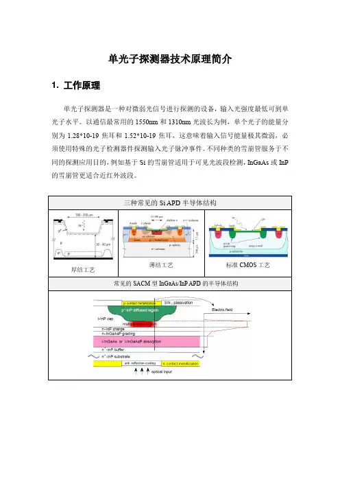
单光子探测器技术原理简介1. 工作原理单光子探测器是一种对微弱光信号进行探测的设备,输入光强度最低可到单光子水平。
以通信最常用的1550nm和1310nm光波长为例,单个光子的能量分别为1.28*10-19焦耳和1.52*10-19焦耳,这意味着输入信号能量极其微弱,必须使用特殊的光子检测器件探测输入光子脉冲事件。
不同种类的雪崩管服务于不同的探测应用目的,例如基于Si的雪崩管适用于可见光波段检测,InGaAs或InP 的雪崩管更适合近红外波段。
薄结工艺标准CMOS工艺厚结工艺常见的SACM型InGaAs/InP APD的半导体结构数据来自Micro Photon Devices公司数据来自Perkin Elmer公司单光子探测器的工作原理是利用工作于盖革模式(Geiger Mode)下的InGaAs/InP雪崩光电二极管(APD)进行单光子探测。
所谓盖革模式是指APD 工作时要加反向偏压,偏压幅度略微超过雪崩阈值电压,盖革模式与线性模式的区别在于能够将微弱光生载流子放大产生宏观电流。
根据对APD施加偏压的波形,将探测器分为门控工作模式和自由运行模式两类。
光子入射到APD内部引发雪崩,产生微弱雪崩电流脉冲。
探测器内部处理电路采用跨导放大器将微弱电流脉冲转换成电压脉冲并放大、整形,再经过甄别、死时间处理后输出电平、宽度固定的数字脉冲,探测器有脉冲输出表示检测到了输入单光子或微弱光脉冲,而脉冲前沿位置代表光子输入时刻。
光子输入事件及其发生事件正是量子信息、单光子雷达等应用关注的最重要内容,单位时间内计数值则反映了输入光强度。
入射光子引发雪崩发生后,必须尽快将雪崩淬灭,一方面避免雪崩管过度放电,更重要的是将雪崩管恢复到可用状态,能够及时检测下一个入射光子事件。
根据淬灭方式的不同,将探测器分为主动淬灭和被动淬灭两类。
通过空间耦合光内部集成了TEC,耦合光纤输入耦合光纤,需外部配置TEC量子通信主流技术是基于通信光纤的方案,与常规通信一样远距离传输必然使用单模光纤,例如电信基础设施建设广泛应用的G.652单模光纤。
基于InGaAs(P)InP APD的单光子探测器的研制和性能研究
基于InGaAs(P)/InP APD的单光子探测器的研制和性能研究单光子探测器是目前量子信息领域、激光雷达和生物医学等领域的关键器件。
基于InGaAs(P)/InP雪崩光电二极管(APD)的单光子探测器适用于近红外波段,制冷要求低,响应速度快,体积小巧,光纤与器件耦合较容易,实用性较强。
然而,相对于超导纳米线等性能更高的探测器以及用于可见光波段探测的光电倍增管和SiAPD,基于InGaAs(P)/InPAPD的单光子探测器的主要缺点在于其探测效率相对偏低,后脉冲概率较大。
单光子探测器常用于量子通信、激光雷达、荧光寿命分析等应用,不同应用对探测器的性能和工作条件要求差别较大,且其各项性能指标受外部参数影响较大。
研究单光子探测器的性能与其工作模式和参数的关系,特别是后脉冲效应与各参数的关系,针对不同应用系统研究不同侧重点的单光子探测技术,具有重要的研究意义和应用价值。
本论文研制了基于InGaAs(P)/InPAPD的近红外自由运转单光子探测器和门控单光子探测器,对其性能的测试方法和影响因素进行了研究,重点针对后脉冲效应进行了深入研究,并在激光测距系统应用中比较了两种探测器的性能及其对系统性能的影响。
主要的研究内容如下:1.综合现有猝灭恢复电路的优点,设计了超低延迟的主动猝灭主动恢复(AQAR)电路,研制了高性能的自由运转单光子探测器。
设计了在APD的阳极或阴极进行雪崩提取和猝灭的多种不同AQAR电路组合,不同电路组合具有不同的猝灭延迟和不同的最大过偏压。
对不同电路组合的雪崩猝灭性能进行了比较研究,并以此为指导对电路结构进行改进。
利用商用SiGe集成电路比较器、高速E-pHEMT射频晶体管和电容平衡噪声抑制电路设计了超低延迟的AQAR电路,其中巧妙地利用了比较器自身的锁存功能实现雪崩后猝灭状态的锁存,降低了反馈环路延迟;引入了电容平衡法,较好地消除了微分噪声。
改进的AQAR电路使雪崩持续时间短至约1ns,显著提高了自由运转探测器的性能。
超导纳米线单光子探测器原理及应用-v4
目
录
摘要.............................................................................................................1 1 简介.......................................................................................................3 1.1 1.2 2 超导光辐射检测技术 .................................................................3 单光子检测:基本原理和评判依据 .........................................4
4
总结.....................................................................................................23
1 简介
1.1 超导光辐射检测技术
100 年前,荷兰人 Onnes 发现了神奇的超导现象【1】 ,超导应用发展进 程也从此拉开序幕。超导态对光波段的辐射较为敏感【2】 ,1994 年人类首次 成功实现了超导辐射探测器和超导测辐射热仪【3】 ,这得益于超导薄膜、微 加工技术和激光光源等学科的发展。在天文等领域的需求牵引下,出现了一 系列具有单光子灵敏度能量分辨率的超导探测器,它们工作温度通常在 1 开 尔文以下。 这类探测器包括: 超导隧道结 (STJ: superconducting tunnel junction) 【4】 ,电阻转变沿探测器(TES: transition edge sensor) 【5】和动态电感探测 器(KID: kinetic inductance detector) 【6】 。 十年前,Gol’tsman 等人利用氮化铌(NbN)纳米线首次验证了一类新 概念的超导探测器【7】 。这类探测器在可见光和近红外波段具有单光子灵敏 度,且其恢复时间和定时精度比现有的基于超导材料的单光子探测器具有数 量级的提升, 被称为超导单光子探测器 (SSPD: superconducting single-photon detector )或超导纳米线单光子探测器( SNSPD : superconducting nanowire single-photon detector)*。此外,这类探测器可以工作在液氦温区(4.2K) , 是较为成熟的闭合循环(机械)制冷技术可以实现的温度区间【8】 。SNSPD 在红外波段时间关联单光子计数( TCSPC : time correlated single-photon counting) 【9】方面具有很大的应用潜力,该领域已开始出现很多新的重要 应 用。 SNSPD 的主要竞争对手是固态单光子雪崩光电二极管( SPAD: single-photon avalanche photodiode ) 。 而 大 尺 寸 的 光 电 倍 增 管 ( PMT: photomultipliers) 【10】目前已经被 SPAD 所取代。SNSPD 的波长响应范围 远高于硅 SPAD【11】 ;和 InGaAs SPAD【12】相比,SNSPD 在性噪比方面 具有明显的优势。SNSPD 在过去十年内已经成为一个研究的热点领域。目 前世界上很多研究小组都在开展相关的研究工作,并不断推动这个领域的发 展。本综述文章将概要介绍器件的工作原理、器件结构设计、制冷、器件材 料以及应用研究进展。
广东工业大学-InGaAs-APD特性研究及1310nm单光子探测
p h o t o n d e t e c t i o n , b u t t o o l o w t e m p e r a t u r e i s n o t g o o d f o r d e t e c t i o n b e c a u s e o f a f t e r p u l s e a n d t h e b r e a k d o w n v o l t a g e . We a l s o d e s i g n e d t h e s i n g l e p h o t o n d e t e c t o r u s i n g t h e t r a n s i m p e d a n c e a m p l i f i e r , w h i c h i s d i f f e r e n t f r o m
越来越低。 一种能够彻底防范第三者窃听的技术,己经越来越成为军事、 外交、商贸等领域的迫切需要。量子保密通信是密码学和量子力学相结 合的产物,它的安全性由量子力学基本原理一一测不准原理和单量子态 不可克隆定理所保证 ,因而越来越受到人们的重视。量子通信的关键技
术之一就是红外 ( 1 3 1 0 n m. 1 5 5 0 n m)单光子探测, 这是因为光量子密钥
c r y p t o g r a p h y t o e n s u r e t h e s e c u r i t y o f c o m mu n i c a t i o n . T o d a y ' s
c r y p t o g r a p h y t e c h n o l o g y i s v e r y s a f e , h o w e v e r , w i t h t h e d e v e l o p m e n t o f
四象限InGaAs APD探测器的研究
四象限InGaAs APD探测器的研究
王致远;李发明;刘方楠
【期刊名称】《光通信研究》
【年(卷),期】2007(000)006
【摘要】文章中设计的四象限InGaAs雪崩光电二极管(Avalanche Photo Diode,APD)的管芯结构采用正入光式平面型结构,而材料结构采用吸收区、倍增区渐变分离的APD结构,在对响应时间、暗电流和响应度等参数进行计算与分析的基础上,优化了器件结构参数.试验结果表明,其响应时间≤1.5 ns,响应度≥9.5 A/W,暗电流≤40 nA,可靠性设计时使PN结和倍增层均在器件表面以下,可有效抑制器件表面漏电流,提高器件的可靠性.
【总页数】4页(P43-46)
【作者】王致远;李发明;刘方楠
【作者单位】重庆邮电大学,光电工程学院,重庆,400065;重庆邮电大学,光电工程学院,重庆,400065;重庆邮电大学,光电工程学院,重庆,400065
【正文语种】中文
【中图分类】TN3
【相关文献】
1.InGaAs/InP APD探测器光电特性检测 [J], 肖雪芳;杨国华;归强;王国宏;马晓宇;陈朝;陈良惠
2.InGaAs/InGaAsP/InP SAGM-APD室温下静态光电特性的研究 [J], 丁国庆
3.Ge-APD及InGaAs/InGaAsP/InP SAGM-APD的暗电流-温度特性及其比较[J], 丁国庆
4.长距离高比特率光纤通信用InGaAs/InGaAsP/InP SAGM-APD [J], 林洪榕
5.InGaAs四象限探测器 [J], 莫才平;高新江;王兵
因版权原因,仅展示原文概要,查看原文内容请购买。
外文翻译---用于量子密钥的单光子APD探测器设计
Design and Characterization of Single Photon APD Detector forQKD ApplicationAbstractModeling and design of a single photon detector and its various characteristics are presented. It is a type of avalanche photo diode (APD) designed to suit the requirements of a Quantum Key Distribution (QKD) detection system. The device is modeled to operate in a gated mode at liquid nitrogen temperature for minimum noise and maximum gain. Different types of APDs are compared for best performance. The APD is part of an optical communication link, which is a private channel to transmit the key signal. The encrypted message is sent via a public channel. The optical link operates at a wavelength of 1.55μm. The design is based on InGaAs with a quantum efficiency of more than 75% and a multiplication factor of 1000. The calculated dark current is below 10-12A with an overall signal to noise ratio better than 18dB. The device sensitivity is better than -40dBm, which is more than an order of magnitude higher than the dark current, corresponding to a detection sensitivity of two photons in pico-second pulses.I. INTRODUCTIONPhoton detectors sensitive to extremely low light levels are needed in a variety of applications. It was not possible to introduce these devices commercially several years ago because of the stringent requirements of QKD. Research efforts however resulted in photon detectors with reasonably good performance characteristics. The objective here is to model a single photon detector of high sensitivity, suitable for a QKD system. The detector is basically an APD, which needs cooling to very low temperature (77K) for the dark current to be low. The wavelength of interest is 1.55μm. Different applications may impose different requirements, and hence the dependence of the various parameters on wavelength, temperature, responsivity, dark current, noise etc, are modeled. Comparison of the results from calculations based on a suitable model provides amenable grounds to determine the suitability of each type of APD for a specific application.Attacks on communication systems in recent years have become a main concern accompanying the technological advances. The measures and counter measures against attacks have driven research effort towards security techniques that aim at absolute infallibility. Quantum Mechanics is considered one of the answers, due to inherent physical phenomena. QKD systems which depend on entangled pairs orpolarization states will inevitably require the usage of APDs in photon detection systems. How suitable these detectors may be, depends on their ability to detect low light level signals, in other words “photon counting”. It is therefore anticipated that the application of high security systems will be in high demand in a variety of fields such as banking sector, military, medical care, e-commerce, e-government etc.Ⅱ. AV ALANCHE PHOTO DIODEA. Structure of the APDFig. 1 shows a schematic diagram of the structure of an APD. The APD is a photodiode with a built-in amplification mechanism. The applied reverse potential difference causes accelerates photo-generated carriers to very high speeds so that a transfer of momentum occurs upon collisions, which liberates other electrons. Secondary electrons are accelerated in turn and the result is an avalanche process. The photo generated carriers traverse the high electric field region causing further ionization by releasing bound electrons in the valence band upon collision. This carrier generation mechanism is known as impact ionization. When carriers collide with the crystal lattice, they lose some energy to the crystal. If the kinetic energy of a carrier is greater than the band-gap, the collision will free a bound electron. The free electrons and holes so created also acquire enough energy to cause further impact ionization. The result is an avalanche, where the number of free carriers grows exponentially as the process continues.The number of ionization collisions per unit length for holes and electrons is designated ionization coefficients αn and αp, respectively. The type of materials and their band structures are responsible for the variation in αn and αp. Ionization coefficients also depend on the applied electric field according tothe following relationship:,exp[]n p b a Eαα=- (1) For αn = αp = α, the multiplication factor, M takes the form11aW M -= (2)W is the width of the depletion region. It can be observed that M tends to ∞ when αW →1, whichsignifies the condition for junction breakdown. Therefore, the high values of M can be obtained whenthe APD is biased close to the breakdown region.The thickness of the multiplication region for M = 1000, has been calculated and compared withthose found by other workers and the results are shown in Table 1. The layer thickness for undoped InPis 10μm, for a substrate thickness of 100μm .The photon-generated electron-hole pairs in the absorption layer are accelerated under theinfluence of an electric field of 3.105V/cm. The acceleration process is constantly interrupted by randomcollisions with the lattice. The two competing processes will continue until eventually an averagesaturation velocity is reached. Secondary electron-hole pairs are generated at any time during theprocess, when they acquire energy larger than the band gap Eg. The electrons are then accelerated andmay cause further impact ionization.Impact ionization of holes due to bound electrons is not as effective as that due to free electrons.Hence, most of the ionization is achieved by free electrons. The avalanche process then proceedsprincipally from the p to the n side of the device. It terminates after a certain time, when the electronsarrive at the n side of the depletion layer. Holes moving to the left create electrons that move to the right,which in turn generate further holes moving to the left in a possibly unending circulation. Although this feedback process increases the gain of the device, it is nevertheless undesirable for several reasons. First, it is time consuming and reduces the device bandwidth. Second, it is a random process and therefore increases the noise in the device. Third, it is unstable, which may cause avalanche breakdown.It may be desirable to fabricate APDs from materials that permit impact ionization by only one type of carriers either electrons or holes. Photo detector materials generally exhibit different ionization rates for electrons and holes. The ratio ofthe two ionization rates k = βi/αi is a measure of the photodiode performance. If for example, electrons have higher ionization coefficient, optimal behavior is achieved by injecting electrons of photo-carrier pairs at the p-type edge of the depletion layer and by using a material with k value as small as possible. If holes are injected, they should be injected at the n-type edge of the depletion layer and k should be as large as possible. Single-carrier multiplication is achieved ideally, when k = 0 with electrons or with k = ∞for holes.B.Geiger ModeGeiger mode (GM) operation means that the diode is operated slightly above the breakdown threshold voltage, where a single electron–hole pair can trigger a strong avalanche. In the case of such an event, the electronics reduce the diode voltage to below the threshold value for a short time called “dead time”, during which the avalanche is stopped and the detector is made ready to detect the next batch of photons. GM operation is one of the basic of Quantum Counting techniques when utilizing an avalanche process (APD) that increases the detector efficiency significantly.There are a number of parameters related to Geiger mode. The general idea however is to temporarily disturb the equilibrium inside the APD.The Geiger mode is placing the APD in a gated regime and the bias is raised above the breakdownvoltage for a short period of time. Fig. 2 shows the parameters characterizing the Geiger operation. The rise and fall times of the edges are neglected because they are made fast. Detection of single photons occurs during the gate window.作者:Khalid A. S. Al-Khateeb, Nazmus Shaker Nafi, Khalid Hasan国籍:美国出处:Computer and Communication Engineering (ICCCE), 2010 International Conference on 11-12 May 2010用于量子密钥的单光子APD探测器设计摘要本文提出的是单光子探测器及其各种特性的建模与设计。