NI-PXIe4496数据采集卡中文翻译
NI PCI-6143数据采集卡产品规格
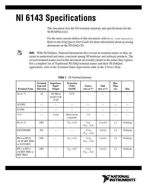
NI 6143 SpecificationsThis document lists the I/O terminal summary and specifications for theNI PCI/PXI-6143.For the most current edition of this document, refer to /manuals.Refer to the DAQ Quick Start Guide for more information about accessingdocuments on the NI-DAQ CD.Note With NI-DAQmx, National Instruments has revised its terminal names so they areeasier to understand and more consistent among NI hardware and software products. Therevised terminal names used in this document are usually similar to the names they replace.For a complete list of Traditional NI-DAQ terminal names and their NI-DAQmxequivalents, refer to the Terminal Name Equivalents table in the S Series Help.Table 1. I/O Terminal SummaryTerminal Name TerminalType andDirectionImpedanceInput/OutputProtection(Volts)On/OffSource(mA at V)Sink(mAat V)RiseTime(ns)BiasAI <0..7>AI100 MΩ inparallel with10 pF15/15————AI GND———————D GND———————+5 V—0.1 ΩShort-circuitto ground1A———P0.<0..7>DIO—V CC+0.58 at(V CC–0.4)11 at 0.4 1.150kΩ puEXTSTROBE*DO—— 3.5 at(V CC–0.4)5 at 0.4 1.550kΩ puPFI 0 or PFI 0/ (AI START TRIG or AI START)DIO—V CC+0.5 3.5 at(V CC–0.4)5 at 0.4 1.550kΩ puPFI 1 or PFI1/ (AI REF TRIG or REF TRIG)DIO—V CC+0.5 3.5 at(V CC–0.4)5 at 0.4 1.550kΩ puNI 6143 Specifications PFI 2DIO —V CC +0.5 3.5 at (V CC –0.4) 5 at 0.4 1.550k Ω pu PFI 3 or PFI 3/ (CTR 1 SOURCE or CTR 1 SRC)DIO—V CC +0.53.5 at (V CC –0.4) 5 at 0.41.550k Ω puPFI 4 or PFI 4/ CTR 1 GATE DIO —V CC +0.53.5 at (V CC –0.4) 5 at 0.4 1.550k Ω pu CTR 1 OUT DO —— 3.5 at (V CC –0.4) 5 at 0.4 1.550k Ω pu PFI 5 or PFI 5/ (AO SAMP CLK or AO SAMP)DIO—V CC +0.53.5 at (V CC –0.4) 5 at 0.41.550k Ω puPFI 6 or PFI 6/ (AO START TRIG or AO START)DIO —V CC +0.53.5 at (V CC –0.4) 5 at 0.4 1.550k Ω puPFI 7 or PFI 7/ (AI SAMP CLK or AI SAMP)DIO —V CC +0.53.5 at (V CC –0.4) 5 at 0.4 1.550k Ω puPFI 8 or PFI 8/ (CTR 0 SOURCE or CTR 0 SRC)DIO —V CC +0.53.5 at (V CC –0.4) 5 at 0.4 1.550k Ω puPFI 9 or PFI 9/ CTR 0 GATE DIO —V CC +0.53.5 at (V CC –0.4) 5 at 0.4 1.550k Ω pu CTR 0 OUT DO —— 3.5 at (V CC –0.4) 5 at 0.4 1.550k Ω pu FREQ OUT or F OUTDO——3.5 at (V CC –0.4)5 at 0.41.550k Ω pu* Indicates active lowAI = Analog Input DIO = Digital Input/Output pu = pull-upAO = Analog Output DO = Digital OutputNote : The tolerance on the 50k Ω pull-up resistors is large. Actual value might range between 17k Ω and 100k Ω.Table 1. I/O Terminal Summary (Continued)Terminal Name Terminal Type and Direction Impedance Input/ OutputProtection (Volts) On/Off Source (mA at V)Sink (mA at V)Rise Time (ns)BiasSpecificationsThe following specifications are typical at 25°C unless otherwise noted. Analog InputInput CharacteristicsNumber of channels...............................8 differentialADC resolution......................................16 bits, 1 in 65,536Sampling rateMaximum........................................250 kS/sMinimum........................................0 S/sAccuracy.........................................±50 ppm for internal timebaseInput coupling........................................DCInput range.............................................±5 VInput impedanceAI + to AI GND..............................100 MΩ in parallel with 10 pFAI – to AI GND..............................100 MΩ in parallel with 10 pFInput bias current...................................±20 pA typ, ±150 pA maxInput offset current.................................±3 pA typ, ±20 pA maxMax working voltage for all analog input channelsPositive input (AI +).......................±7 VNegative input (AI –)......................±7 VOvervoltage protection(AI +, AI –)............................................±15 VInput current duringovervoltage conditions...........................±5.7 mA maxInput FIFO size......................................2,046 samplesData transfers.........................................DMA, interrupts,programmed I/ODMA mode............................................Scatter-gather© National Instruments Corporation3NI 6143 SpecificationsNI 6143 Specifications DC Transfer CharacteristicsDNL........................................................±0.8 LSB typ, no missing codes INL..........................................................±1.5 LSB typ, ±3.0 LSB max System noise...........................................0.8 LSB rmsDynamic CharacteristicsPhase mismatch......................................±0.5° at 100 kHz Crosstalk.................................................–90 dB at 50 kHz Bandwidth...............................................490 kHz SINAD....................................................89 dB at 10 kHz CMRR.....................................................75 dB at 60 Hz SFDR......................................................98 dB at 10 kHz THD........................................................–96 dBc at 10 kHzStabilityRecommended warm-up time.................15 min Onboard Calibration ReferenceLevel................................................2.50 V (±2.5 mV)(actual value stored in EEPROM)Temperature coefficient...................±7.0 ppm/°C max Long-term stability..........................±20 ppm/Table 2. NI 6143 Analog Input DC Accuracy InformationNominal Range at Full Scale (V)Absolute AccuracyGain Error (%of Reading)Offset +INL Error (µV)Gain Tempco Ext./Int. Cal (%/°C)Offset Tempco (µV/°C)Random Noise (µV rms )Absolute Accuracy at Full Scale (mV)Relative Accuracy (mV)±5.00.056000.0007/0.00031041223.6130.0488Note : Accuracies are valid for measurements following an internal S Series calibration. Averaged numbers assume averaging of 100 single-channel readings. Measurement accuracies are listed for operational temperatures within ±1°C of internal calibration temperature and ±10 °C of external or factory-calibration temperature. NI recommends a one-year calibration interval. The Absolute Accuracy at Full Scale calculations were performed for a maximum range input after one year and 100points of averaged data.1,000 hTypical Performance Graphs© National Instruments Corporation5NI 6143 SpecificationsNI 6143 Specifications Digital I/ONumber of channels................................8 input/output Compatibility..........................................TTL/CMOSPower-on state........................................Input (high-impedance)Data transfers..........................................DMA, interrupts,programmed I/OTiming I/OCounter/TimersNumber of channels................................2 up/down counter/timers Resolution...............................................24 bits Compatibility..........................................TTL/CMOSTable 3. Digital Logic LevelsLevelMin Max Input low voltage Input high voltageInput low current (V in = 0 V)Input high current (V in = 5 V)0.0 V 2.2 V ——0.8 V 5.0 V –320 µA 10 µA Output low voltage (I OL = 24 mA) Output low voltage (I OL = 11 mA)Output low voltage (I OL = –13 mA)Output high voltage (I OH = –8 mA)——4.1 V 4.35 V0.83 V 0.4 V ——Table 4. Digital Logic LevelsLevelMin Max Input low voltage Input high voltage0.0 V 2.2 V 0.8 V 5.0 V Output low voltage (I OL = 5 mA)Output high voltage (I OH = –3.5 mA)—4.35 V0.4 V —Base clock frequency.............................20 MHzBase clock accuracy...............................±0.01%Max source frequency............................20 MHzMin source pulse duration......................10 ns, edge-detect modeMin gate pulse duration..........................10 ns, edge-detect modeData transfers.........................................DMA, interrupts,programmed I/OFrequency ScalerNumber of channels (1)Resolution..............................................4-bitCompatibility.........................................TTL/CMOSDigital logic levels.................................Refer to Table 4Base clock frequency.............................10 MHz, 100 kHzBase clock accuracy...............................±0.01%Digital TriggerPurpose...................................................Start, reference, and pause trigger,sample clockExternal sources.....................................PFI <0..9>, RTSI <0..6>Compatibility.........................................TTLResponse................................................Rising or falling edgePulse width.............................................10 ns minRTSI Bus (PCI Only)Trigger lines <0..6> (7)RTSI clock (1)© National Instruments Corporation7NI 6143 SpecificationsPXI Trigger Bus (PXI Only)Trigger lines <0..5> (6)Star trigger (1)Clock (1)Power Requirement+5 VDC (±5%).......................................40 mA+3.3 VDC (±5%)....................................140 mA+12 VDC (±5%).....................................150 mA–12 VDC (±5%)......................................80 mAPower available at I/O connector............+4.65 to +5.25 VDC at 1 APhysicalDimensions(not including connectors)......................15.5 cm by 10.6 cm(6.10 in. by 4.17 in.)I/O connector..........................................68-pin VHDCIEnvironmentalThe NI 6143 is intended for indoor use only.Operating EnvironmentAmbient temperature range....................0 to 50 °C (tested in accordancewith IEC-60068-2-1 andIEC-60068-2-2)Relative humidity range..........................10 to 90%, noncondensing(tested in accordance withIEC-60068-2-56)Altitude...................................................2,000 m (at 25 °C ambienttemperature)NI 6143 © National Instruments Corporation 9NI 6143 SpecificationsStorage EnvironmentAmbient temperature range....................–20 to 70 °C (tested in accordancewith IEC-60068-2-1 and IEC-60068-2-2)Relative humidity range.........................5 to 95%, noncondensing(tested in accordance with IEC-60068-2-56)Shock and VibrationOperational shock..................................30 g peak, half-sine, 11 ms pulse(Tested in accordance with IEC-60068-2-27. Test profile developed in accordance with MIL-PRF-28800-F.)Random vibrationOperating ........................................5 to 500 Hz, 0.3 g rmsNonoperating ..................................5 to 500 Hz, 2.4 g rms(Tested in accordance with IEC-60068-2-64. Nonoperating test profile exceeds the requirements ofMIL-PRF-28800-F, Class 3.)Note Clean the device with a soft, non-metallic brush. Make sure that the device iscompletely dry and free from contaminants before returning it to service.SafetyThis product is designed to meet the requirements of the following standards of safety for electrical equipment for measurement, control, and laboratory use:•IEC 61010-1, EN 61010-1•UL 3111-1, UL 61010B-1•CAN/CSA C22.2 No. 1010.1Note For UL and other safety certifications, refer to the product label, or visit /hardref.nsf , search by model number or product line, and click theappropriate link in the Certification column.National Instruments™, NI™, ™, NI-DAQ™, and RTSI™ are trademarks of National Instruments Corporation. Product and company names mentioned herein are trademarks or trade names of their respective companies. For patents covering National Instruments products, refer to the appropriate location: Help»Patents in your software, the patents.txt file on your CD, or /patents .© 2004 National Instruments Corp. All rights reserved.370835A-01Feb04*370835A-01*Electromagnetic CompatibilityEmissions................................................EN 55011 Class A at 10 mFCC Part 15A above 1 GHz Immunity ................................................EN 61326:1997A2:2001, Table 1EMC/EMI...............................................CE, C-Tick, and FCC Part 15(Class A) CompliantNote For EMC compliance, you must operate this device with shielded cabling.CE ComplianceThis product meets the essential requirements of applicable European Directives, as amended for CE marking, as follows:Low-Voltage Directive (safety).............. 73/23/EEC Electromagnetic CompatibilityDirective (EMC)..................................... 89/336/EECNote Refer to the Declaration of Conformity (DoC) for this product for any additionalregulatory compliance information. To obtain the DoC for this product, visit /hardref.nsf , search by model number or product line, and click theappropriate link in the Certification column.。
基于LabVIEW的数据采集卡PXIe-4499自动校准系统
基于LabVIEW的数据采集卡PXIe-4499自动校准系统沈介明
【期刊名称】《电子产品可靠性与环境试验》
【年(卷),期】2017(035)0z1
【摘要】首先,通过GPIB/GPIB线和USB/GPIB线将FLUKE5522A、
Agilent33120A、PXIe-1062Q控制器和PXIe-4499数据采集卡连接组成了硬件系统;然后,在图形化编程软件LabVIEW和虚拟仪器驱动程序的基础上,设计了数据采集卡PXIe-4499自动校准系统,该系统能够提高数据采集卡的校准效率,具有一定的推广价值.
【总页数】5页(P100-104)
【作者】沈介明
【作者单位】工业和信息化部电子第五研究所华东分所,江苏苏州201705
【正文语种】中文
【中图分类】TP274+.2
【相关文献】
1.一种数据采集卡自动校准系统及关键技术研究 [J], 刘天时;龙文;马宇
2.基于LabVIEW平台的通用数据采集卡的驱动方法及数据采集 [J], 李威宣;黄建新
3.基于LabVIEW控制的频谱分析仪自动校准系统的探究 [J], 申龙
4.基于LabVIEW的某推力自动校准系统 [J], 王得志;方俊雅
5.基于LabVIEW控制的频谱分析仪自动校准系统的探究 [J], 申龙
因版权原因,仅展示原文概要,查看原文内容请购买。
NI PCI-6143数据采集卡产品规格
NI 6143 SpecificationsThis document lists the I/O terminal summary and specifications for theNI PCI/PXI-6143.For the most current edition of this document, refer to /manuals.Refer to the DAQ Quick Start Guide for more information about accessingdocuments on the NI-DAQ CD.Note With NI-DAQmx, National Instruments has revised its terminal names so they areeasier to understand and more consistent among NI hardware and software products. Therevised terminal names used in this document are usually similar to the names they replace.For a complete list of Traditional NI-DAQ terminal names and their NI-DAQmxequivalents, refer to the Terminal Name Equivalents table in the S Series Help.Table 1. I/O Terminal SummaryTerminal Name TerminalType andDirectionImpedanceInput/OutputProtection(Volts)On/OffSource(mA at V)Sink(mAat V)RiseTime(ns)BiasAI <0..7>AI100 MΩ inparallel with10 pF15/15————AI GND———————D GND———————+5 V—0.1 ΩShort-circuitto ground1A———P0.<0..7>DIO—V CC+0.58 at(V CC–0.4)11 at 0.4 1.150kΩ puEXTSTROBE*DO—— 3.5 at(V CC–0.4)5 at 0.4 1.550kΩ puPFI 0 or PFI 0/ (AI START TRIG or AI START)DIO—V CC+0.5 3.5 at(V CC–0.4)5 at 0.4 1.550kΩ puPFI 1 or PFI1/ (AI REF TRIG or REF TRIG)DIO—V CC+0.5 3.5 at(V CC–0.4)5 at 0.4 1.550kΩ puNI 6143 Specifications PFI 2DIO —V CC +0.5 3.5 at (V CC –0.4) 5 at 0.4 1.550k Ω pu PFI 3 or PFI 3/ (CTR 1 SOURCE or CTR 1 SRC)DIO—V CC +0.53.5 at (V CC –0.4) 5 at 0.41.550k Ω puPFI 4 or PFI 4/ CTR 1 GATE DIO —V CC +0.53.5 at (V CC –0.4) 5 at 0.4 1.550k Ω pu CTR 1 OUT DO —— 3.5 at (V CC –0.4) 5 at 0.4 1.550k Ω pu PFI 5 or PFI 5/ (AO SAMP CLK or AO SAMP)DIO—V CC +0.53.5 at (V CC –0.4) 5 at 0.41.550k Ω puPFI 6 or PFI 6/ (AO START TRIG or AO START)DIO —V CC +0.53.5 at (V CC –0.4) 5 at 0.4 1.550k Ω puPFI 7 or PFI 7/ (AI SAMP CLK or AI SAMP)DIO —V CC +0.53.5 at (V CC –0.4) 5 at 0.4 1.550k Ω puPFI 8 or PFI 8/ (CTR 0 SOURCE or CTR 0 SRC)DIO —V CC +0.53.5 at (V CC –0.4) 5 at 0.4 1.550k Ω puPFI 9 or PFI 9/ CTR 0 GATE DIO —V CC +0.53.5 at (V CC –0.4) 5 at 0.4 1.550k Ω pu CTR 0 OUT DO —— 3.5 at (V CC –0.4) 5 at 0.4 1.550k Ω pu FREQ OUT or F OUTDO——3.5 at (V CC –0.4)5 at 0.41.550k Ω pu* Indicates active lowAI = Analog Input DIO = Digital Input/Output pu = pull-upAO = Analog Output DO = Digital OutputNote : The tolerance on the 50k Ω pull-up resistors is large. Actual value might range between 17k Ω and 100k Ω.Table 1. I/O Terminal Summary (Continued)Terminal Name Terminal Type and Direction Impedance Input/ OutputProtection (Volts) On/Off Source (mA at V)Sink (mA at V)Rise Time (ns)BiasSpecificationsThe following specifications are typical at 25°C unless otherwise noted. Analog InputInput CharacteristicsNumber of channels...............................8 differentialADC resolution......................................16 bits, 1 in 65,536Sampling rateMaximum........................................250 kS/sMinimum........................................0 S/sAccuracy.........................................±50 ppm for internal timebaseInput coupling........................................DCInput range.............................................±5 VInput impedanceAI + to AI GND..............................100 MΩ in parallel with 10 pFAI – to AI GND..............................100 MΩ in parallel with 10 pFInput bias current...................................±20 pA typ, ±150 pA maxInput offset current.................................±3 pA typ, ±20 pA maxMax working voltage for all analog input channelsPositive input (AI +).......................±7 VNegative input (AI –)......................±7 VOvervoltage protection(AI +, AI –)............................................±15 VInput current duringovervoltage conditions...........................±5.7 mA maxInput FIFO size......................................2,046 samplesData transfers.........................................DMA, interrupts,programmed I/ODMA mode............................................Scatter-gather© National Instruments Corporation3NI 6143 SpecificationsNI 6143 Specifications DC Transfer CharacteristicsDNL........................................................±0.8 LSB typ, no missing codes INL..........................................................±1.5 LSB typ, ±3.0 LSB max System noise...........................................0.8 LSB rmsDynamic CharacteristicsPhase mismatch......................................±0.5° at 100 kHz Crosstalk.................................................–90 dB at 50 kHz Bandwidth...............................................490 kHz SINAD....................................................89 dB at 10 kHz CMRR.....................................................75 dB at 60 Hz SFDR......................................................98 dB at 10 kHz THD........................................................–96 dBc at 10 kHzStabilityRecommended warm-up time.................15 min Onboard Calibration ReferenceLevel................................................2.50 V (±2.5 mV)(actual value stored in EEPROM)Temperature coefficient...................±7.0 ppm/°C max Long-term stability..........................±20 ppm/Table 2. NI 6143 Analog Input DC Accuracy InformationNominal Range at Full Scale (V)Absolute AccuracyGain Error (%of Reading)Offset +INL Error (µV)Gain Tempco Ext./Int. Cal (%/°C)Offset Tempco (µV/°C)Random Noise (µV rms )Absolute Accuracy at Full Scale (mV)Relative Accuracy (mV)±5.00.056000.0007/0.00031041223.6130.0488Note : Accuracies are valid for measurements following an internal S Series calibration. Averaged numbers assume averaging of 100 single-channel readings. Measurement accuracies are listed for operational temperatures within ±1°C of internal calibration temperature and ±10 °C of external or factory-calibration temperature. NI recommends a one-year calibration interval. The Absolute Accuracy at Full Scale calculations were performed for a maximum range input after one year and 100points of averaged data.1,000 hTypical Performance Graphs© National Instruments Corporation5NI 6143 SpecificationsNI 6143 Specifications Digital I/ONumber of channels................................8 input/output Compatibility..........................................TTL/CMOSPower-on state........................................Input (high-impedance)Data transfers..........................................DMA, interrupts,programmed I/OTiming I/OCounter/TimersNumber of channels................................2 up/down counter/timers Resolution...............................................24 bits Compatibility..........................................TTL/CMOSTable 3. Digital Logic LevelsLevelMin Max Input low voltage Input high voltageInput low current (V in = 0 V)Input high current (V in = 5 V)0.0 V 2.2 V ——0.8 V 5.0 V –320 µA 10 µA Output low voltage (I OL = 24 mA) Output low voltage (I OL = 11 mA)Output low voltage (I OL = –13 mA)Output high voltage (I OH = –8 mA)——4.1 V 4.35 V0.83 V 0.4 V ——Table 4. Digital Logic LevelsLevelMin Max Input low voltage Input high voltage0.0 V 2.2 V 0.8 V 5.0 V Output low voltage (I OL = 5 mA)Output high voltage (I OH = –3.5 mA)—4.35 V0.4 V —Base clock frequency.............................20 MHzBase clock accuracy...............................±0.01%Max source frequency............................20 MHzMin source pulse duration......................10 ns, edge-detect modeMin gate pulse duration..........................10 ns, edge-detect modeData transfers.........................................DMA, interrupts,programmed I/OFrequency ScalerNumber of channels (1)Resolution..............................................4-bitCompatibility.........................................TTL/CMOSDigital logic levels.................................Refer to Table 4Base clock frequency.............................10 MHz, 100 kHzBase clock accuracy...............................±0.01%Digital TriggerPurpose...................................................Start, reference, and pause trigger,sample clockExternal sources.....................................PFI <0..9>, RTSI <0..6>Compatibility.........................................TTLResponse................................................Rising or falling edgePulse width.............................................10 ns minRTSI Bus (PCI Only)Trigger lines <0..6> (7)RTSI clock (1)© National Instruments Corporation7NI 6143 SpecificationsPXI Trigger Bus (PXI Only)Trigger lines <0..5> (6)Star trigger (1)Clock (1)Power Requirement+5 VDC (±5%).......................................40 mA+3.3 VDC (±5%)....................................140 mA+12 VDC (±5%).....................................150 mA–12 VDC (±5%)......................................80 mAPower available at I/O connector............+4.65 to +5.25 VDC at 1 APhysicalDimensions(not including connectors)......................15.5 cm by 10.6 cm(6.10 in. by 4.17 in.)I/O connector..........................................68-pin VHDCIEnvironmentalThe NI 6143 is intended for indoor use only.Operating EnvironmentAmbient temperature range....................0 to 50 °C (tested in accordancewith IEC-60068-2-1 andIEC-60068-2-2)Relative humidity range..........................10 to 90%, noncondensing(tested in accordance withIEC-60068-2-56)Altitude...................................................2,000 m (at 25 °C ambienttemperature)NI 6143 © National Instruments Corporation 9NI 6143 SpecificationsStorage EnvironmentAmbient temperature range....................–20 to 70 °C (tested in accordancewith IEC-60068-2-1 and IEC-60068-2-2)Relative humidity range.........................5 to 95%, noncondensing(tested in accordance with IEC-60068-2-56)Shock and VibrationOperational shock..................................30 g peak, half-sine, 11 ms pulse(Tested in accordance with IEC-60068-2-27. Test profile developed in accordance with MIL-PRF-28800-F.)Random vibrationOperating ........................................5 to 500 Hz, 0.3 g rmsNonoperating ..................................5 to 500 Hz, 2.4 g rms(Tested in accordance with IEC-60068-2-64. Nonoperating test profile exceeds the requirements ofMIL-PRF-28800-F, Class 3.)Note Clean the device with a soft, non-metallic brush. Make sure that the device iscompletely dry and free from contaminants before returning it to service.SafetyThis product is designed to meet the requirements of the following standards of safety for electrical equipment for measurement, control, and laboratory use:•IEC 61010-1, EN 61010-1•UL 3111-1, UL 61010B-1•CAN/CSA C22.2 No. 1010.1Note For UL and other safety certifications, refer to the product label, or visit /hardref.nsf , search by model number or product line, and click theappropriate link in the Certification column.National Instruments™, NI™, ™, NI-DAQ™, and RTSI™ are trademarks of National Instruments Corporation. Product and company names mentioned herein are trademarks or trade names of their respective companies. For patents covering National Instruments products, refer to the appropriate location: Help»Patents in your software, the patents.txt file on your CD, or /patents .© 2004 National Instruments Corp. All rights reserved.370835A-01Feb04*370835A-01*Electromagnetic CompatibilityEmissions................................................EN 55011 Class A at 10 mFCC Part 15A above 1 GHz Immunity ................................................EN 61326:1997A2:2001, Table 1EMC/EMI...............................................CE, C-Tick, and FCC Part 15(Class A) CompliantNote For EMC compliance, you must operate this device with shielded cabling.CE ComplianceThis product meets the essential requirements of applicable European Directives, as amended for CE marking, as follows:Low-Voltage Directive (safety).............. 73/23/EEC Electromagnetic CompatibilityDirective (EMC)..................................... 89/336/EECNote Refer to the Declaration of Conformity (DoC) for this product for any additionalregulatory compliance information. To obtain the DoC for this product, visit /hardref.nsf , search by model number or product line, and click theappropriate link in the Certification column.。
NI-PXIe4496数据采集卡中文翻译
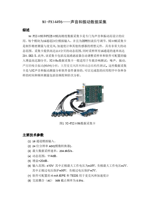
NI-PXI4496——声音和振动数据采集综述NI PXI449X和PXIE449X高精度数据采集卡是专门为声音和振动而设计的应用。
每个模块为16通道24位模拟输入,并且为IEPE恒流信号调节。
NI449X采集卡是制作精密测量与麦克风,加速度计和其他传感器的理想元件,具有非常大的动态范围。
采集卡提供高达114分贝的动态范围,同时采样所有16通道的速率高达204.8KS/S。
此外,该采集卡包括反混淆滤波器自动调整采样率和软件可配置的输入增益高达30分贝。
NI449x数据采集卡一般适用于车载音响测试;噪声,振动,严厉的噪音振动(NVH)分析;大型麦克风阵列和动态结构性测试。
这些数据采集卡是与NI声音和振动测量分析软件套件兼容的,可以完成您的应用程序中各种各样的时间和频率测量包括倍频程和阶次分析。
图1 NI-PXI4496数据采集卡主要技术参数⑴16通道模拟输入。
⑵24位分辨率ADC(模数转换器)。
⑶最大数据采样速率:204.8kS/s。
⑷动态范围:114dB。
⑸增益+20dB。
⑹输入范围:±10V 其中正极最大工作电压为±10V,负极最大工作电压±1V。
其中正极过电压保护±30V,负极过电压保护±5V。
⑺软件可配置的4 mA IEPE和TEDS用于麦克风和加速度计⑻交流耦合(AC)3dB截止频率为0.5hz。
表一 NI4496规格说明表二 NI4496输入/输出表三NI4496 物理标准分析性能:⑼功率谱⑽变焦FFT⑾分数倍频程分析⑿振动级测量⒀谱图⒁瞬态分析技术综述模拟输入操作每一路输入信号都是同时被缓冲,放大,模拟过滤,由24位高精度采样模数转换器(ADC)执行截止频率的数字滤波,自动调整一个软件可编程的采样率。
高分辨率提供了必要的准确性使得NI449x数据采集卡很好的适合音频和振动分析应用程序。
在NI4496中,一个可编程增益放大器在输入阶段提供0dB,20dB增益的选择。
数据采集卡(待完善)

基础知识
方乐 2019年10月23日
什么是数据采集卡?
数据采集是指对设备被测的模拟或数字信号,自动采集并送到上 位机中进行分析、处理。
数据采集卡,即实现数据采集功能的计算机扩展卡,可以通过 USB、PXI、PCI、PCI Express、火线(1394)、PCMCIA、ISA、 Compact Flash、485、232、以太网、各种无线网络等总线接入计算 机。
采样频率:单位时间采集的数据点数,与AD芯片的转换一个点 所需时间有关,例如:AD转换一个点需要T=10us,则其采样频率 f=1/T为100K(即100kHz),即每秒钟AD芯片可以转换100K的数据 点数。常有100K、250K、500K、800K、lM、40M等。
03.技术参数(缓存)
缓存:主要用来存储AD芯片转换后的数据。带缓存板卡可以设 置采样频率,否则不可改变。缓存有RAM和FIFO两种。FIFO主要用 作数据缓冲,存储量不大,速度快;RAM一般用于高速采集卡,存储 量大,速度较慢。
01.分类(处理信号)
③:现在电能计量的常用方法是电能脉冲计量法,即使电能表转盘每 转一圈便输出一个或两个脉冲,用输出的脉冲数代替转盘转动的圈数, 并将脉冲量通过计数器计数后输入测控装置,由CPU进行存储、计算。
01.分类(总线PCI)
PCI是Peripheral Component Interconnect(外设部件互连标准)的缩 写,它是目前个人电脑中使用最为广 泛的接口,几乎所有的主板产品上都 带有这种插槽。PCI插槽也是主板带有 最多数量的插槽类型,在目前流行的 台式机主板上,ATX结构的主板一般 带有5~6个PCI插槽,而小一点的 MATX主板也都带有2~3个PCI插槽, 可见其应用的广泛性。
NI B,E,M,S,X系列数据采集设备校准程序(翻译)
校准程序B/E/M/S/X系列关于NI-DAQ mx这个文件包含了NI-DAQ B/E/M/S/X系列数据采集设备的校准须知。
这个文件没有讨论编程技术或者编译程序。
NI-DAQ mx驱动包含了编译程序须知和详细的函数功能说明的在线帮助文件。
当你在校准计算机上安装NI-DAQ mx后,你能添加这些帮助文件。
内容协议。
2 软件。
3 文档。
3 校准区间。
4 密码。
4 测试设备。
4 测试条件。
6 校准程序。
6 初始化安装。
7 自我校准。
7 设备温度测控。
8 验证程序。
9 模拟输入验证。
10模拟输出验证。
15 计数器验证。
18 调整程序。
20 测试限度。
23 M系列测试极限NI6250/6251/6224/6255/6259----16-位分辨率。
601协议下面是出现在手册中的协议。
》这个引号引导你进入菜单栏,对话框选择最后功能,File>>Page Setup>>Options的顺序引导依次为菜单,安装页,选择,直到最后对话框。
插图显示注释,报警你有重要信息。
图为警告符,建议你采取预防措施,避免损坏设备,数据丢掉,系统破坏。
当符号出现,提及第一安全信息,介绍预防措施。
2Bold 黑粗体正文,你必须选择或链接软件,例如菜单和对话框选择,粗体正文也表示参数名称和硬件标签。
italic斜体正文表示变量,强调参考或介绍一个关键概念,为正文主题,你必须提供一个词或数值形式。
Mono space显示特征,你应从键盘输入片段代号。
例如编程,句法,用于磁盘驱动器的真名,路径,目录,程序,子程序,设备名称,函数,操作,变量,文件名和扩展名。
Mono space italic 这种字体表示斜体文本中的文本,是你必须提供的一个词或数值占位符。
Platform 这种字体的文本显示一个特殊的平台,表明接下来的文本仅应用于那个平台。
软件最新NI-DAQ mx驱动的校准要求。
包括NI-DAQ mx 高级函数调用,以简化的任务来为校准设备写软件。
NI公司按照采样频率排序 采集卡十强
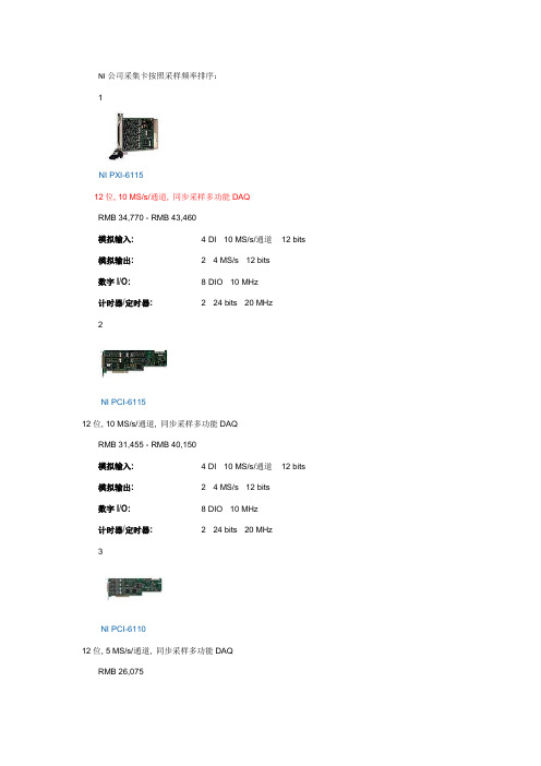
NI公司采集卡按照采样频率排序:1NI PXI-611512位, 10 MS/s/通道, 同步采样多功能DAQRMB 34,770 - RMB 43,460模拟输入: 4 DI · 10 MS/s/通道· 12 bits 模拟输出: 2 · 4 MS/s · 12 bits数字I/O:8 DIO · 10 MHz计时器/定时器: 2 · 24 bits · 20 MHz2NI PCI-611512位, 10 MS/s/通道, 同步采样多功能DAQRMB 31,455 - RMB 40,150模拟输入: 4 DI · 10 MS/s/通道· 12 bits 模拟输出: 2 · 4 MS/s · 12 bits数字I/O:8 DIO · 10 MHz计时器/定时器: 2 · 24 bits · 20 MHz3NI PCI-611012位, 5 MS/s/通道, 同步采样多功能DAQRMB 26,075模拟输入: 4 DI · 5 MS/s/通道· 12 bits 模拟输出: 2 · 4 MS/s · 16 bits数字I/O:8 DIO计时器/定时器: 2 · 24 bits · 20 MHz4NI PCI-611112位, 5 MS/s/通道, 同步采样多功能DAQRMB 19,450模拟输入: 2 DI · 5 MS/s/通道· 12 bits 模拟输出: 2 · 4 MS/s · 16 bits数字I/O:8 DIO计时器/定时器: 2 · 24 bits · 20 MHz5NI PXIe-612416位, 4 MS/s, 同步采样多功能DAQRMB 28,970模拟输入: 4 DI · 4 MS/s/通道· 16 bits 模拟输出: 2 · 4 MS/s · 16 bits数字I/O:24 DIO · 10 MHz计时器/定时器: 2 · 32 bits · 80 MHz6NI PXI-613214位, 3 MS/s/通道, 同步采样多功能DAQRMB 15,725模拟输入: 4 DI · 2.5 MS/s/通道· 14bits数字I/O:8 DIO · 10 MHz计时器/定时器: 2 · 24 bits · 20 MHz测量类型:数字, 频率, 正交编码器,电压7NI PXI-613314位, 3 MS/s/通道, 同步采样多功能DAQRMB 21,935 - RMB 25,245模拟输入:8 DI · 2.5 MS/s/通道· 14 bits 数字I/O:8 DIO · 10 MHz计时器/定时器: 2 · 24 bits · 20 MHz测量类型:数字, 频率, 正交编码器, 电压8NI PCI-613314位, 3 MS/s/通道, 同步采样多功能DAQRMB 21,935 - RMB 25,245模拟输入:8 DI · 2.5 MS/s/通道· 14 bits 数字I/O:8 DIO · 10 MHz计时器/定时器: 2 · 24 bits · 20 MHz测量类型:数字, 频率, 正交编码器, 电压9NI PCI-613214位, 2.5 MS/s/通道, 同步采样多功能DAQRMB 15,725模拟输入: 4 DI · 2.5 MS/s/通道· 14 bits 数字I/O:8 DIO · 10 MHz计时器/定时器: 2 · 24 bits · 20 MHz测量类型:数字, 频率, 正交编码器, 电压10NI PCIe-6363X系列数据采集RMB 13,240模拟输入:32 SE/16 DI · 2 MS/s · 16 bits 模拟输出: 4 · 2.86 MS/s · 16 bits数字I/O:48 DIO · 10 MHz计时器/定时器: 4 · 32 bits · 100 MHz。
ni数据采集卡

ni数据采集卡1. 简介NI数据采集卡(National Instruments Data Acquisition Card)是一种用于采集模拟信号和数字信号的硬件设备。
它可以将外部信号转换为计算机可读取的数字数据,从而实现数据采集、数据处理和数据分析等功能。
NI数据采集卡常用于科学研究、工程应用和实验教学等领域。
2. 功能特点NI数据采集卡具有以下主要功能特点:2.1 模拟信号输入NI数据采集卡可以接收模拟信号的输入,并将其转换为数字信号进行处理。
它具有高精度的模拟输入通道,可适应不同信号类型和信号范围的输入需求。
通过采集卡提供的软件接口,用户可以方便地配置和控制模拟输入参数。
2.2 模拟信号输出除了模拟信号输入功能外,NI数据采集卡还可以输出模拟信号。
用户可以通过采集卡的输出通道,将数字信号转换为模拟信号输出到外部设备,如执行器、显示器等。
这样可以实现对外部设备的控制和观测。
2.3 数字信号输入和输出NI数据采集卡除了支持模拟信号输入输出,还具备数字信号输入输出的功能。
它可以读取和写入数字信号,用于采集和控制数字设备,如开关、传感器等。
数字信号的输入输出通常更快速和稳定,可以满足实时性要求较高的应用需求。
2.4 多通道采集NI数据采集卡通常具有多个模拟输入通道和数字输入通道,可以同时采集多个信号。
这使得它可以广泛应用于多通道数据采集和处理的场景,如声音信号采集、振动信号采集等。
2.5 软件支持NI数据采集卡配套的软件十分强大,可以提供丰富而易用的数据采集和处理功能。
用户可以通过软件界面对采集卡进行配置和控制,实现数据的实时监控、录制和分析。
常见的软件包括NI LabVIEW和NI Measurement Studio等。
3. 应用领域NI数据采集卡广泛应用于以下领域:3.1 科学研究在科学研究领域,NI数据采集卡被广泛应用于物理实验、化学实验、生物实验等。
它可以帮助科研人员采集实验数据,进行数据分析和模型建立。
- 1、下载文档前请自行甄别文档内容的完整性,平台不提供额外的编辑、内容补充、找答案等附加服务。
- 2、"仅部分预览"的文档,不可在线预览部分如存在完整性等问题,可反馈申请退款(可完整预览的文档不适用该条件!)。
- 3、如文档侵犯您的权益,请联系客服反馈,我们会尽快为您处理(人工客服工作时间:9:00-18:30)。
NI-PXI4496——声音和振动数据采集综述NI PXI449X和PXIE449X高精度数据采集卡是专门为声音和振动而设计的应用。
每个模块为16通道24位模拟输入,并且为IEPE恒流信号调节。
NI449X采集卡是制作精密测量与麦克风,加速度计和其他传感器的理想元件,具有非常大的动态范围。
采集卡提供高达114分贝的动态范围,同时采样所有16通道的速率高达204.8KS/S。
此外,该采集卡包括反混淆滤波器自动调整采样率和软件可配置的输入增益高达30分贝。
NI449x数据采集卡一般适用于车载音响测试;噪声,振动,严厉的噪音振动(NVH)分析;大型麦克风阵列和动态结构性测试。
这些数据采集卡是与NI声音和振动测量分析软件套件兼容的,可以完成您的应用程序中各种各样的时间和频率测量包括倍频程和阶次分析。
图1 NI-PXI4496数据采集卡主要技术参数⑴16通道模拟输入。
⑵24位分辨率ADC(模数转换器)。
⑶最大数据采样速率:204.8kS/s。
⑷动态范围:114dB。
⑸增益+20dB。
⑹输入范围:±10V 其中正极最大工作电压为±10V,负极最大工作电压±1V。
其中正极过电压保护±30V,负极过电压保护±5V。
⑺软件可配置的4 mA IEPE和TEDS用于麦克风和加速度计⑻交流耦合(AC)3dB截止频率为0.5hz。
表一 NI4496规格说明表二 NI4496输入/输出表三NI4496 物理标准分析性能:⑼功率谱⑽变焦FFT⑾分数倍频程分析⑿振动级测量⒀谱图⒁瞬态分析技术综述模拟输入操作每一路输入信号都是同时被缓冲,放大,模拟过滤,由24位高精度采样模数转换器(ADC)执行截止频率的数字滤波,自动调整一个软件可编程的采样率。
高分辨率提供了必要的准确性使得NI449x数据采集卡很好的适合音频和振动分析应用程序。
在NI4496中,一个可编程增益放大器在输入阶段提供0dB,20dB增益的选择。
另外,这个数据采集卡包括对换能器电子数据表读写能力的智能传感器以及在软件中选择处理IEPE恒流或者关闭。
NI4496使用的是一种被认为高精度调制的AD转换方法。
采用这种技术,输入信号被过采样或者以几倍于选择的数据率采样,然后应用到数字滤波器。
NI4496数据卡将高精度调制模数转化器一体化,从而在具有优秀的相位线性度的同时保持低噪声和失真。
另外,这类模数转化器可以使采集卡免除与传统数据采集设备相联系的差分非线性的失真。
抗混叠在工程测量中,采样频率不可能无限高也不需要无限高。
在进行动态信号测试中测量仪器必须具有抗混叠功能,采用滤波器滤除高于1/2采样频率的部分,NI4496也不例外。
所有的输入通道在硬件上同时使用模拟和数字滤波器的实现以防止混叠。
信号首先经过固定的模拟过滤器来去除超出模数转化器频率范围之外的信号成分。
然后数字反混叠滤波器自动调整截止频率,来清除任何超过编程采样率一半以上的频率成分。
这个专门的结构就意味着不需要再添加额外的外部滤波器,来防止混叠。
PXI versus PXI ExpressPXI (PCI eXtensions for Instrumentation,面向仪器系统的PCI扩展) 是一种由NI公司发布的坚固的基于PC的测量和自动化平台。
PXI结合了PCI的电气总线特性与CompactPCI的坚固性、模块化及Eurocard机械封装的特性发展成适合于试验、测量与数据采集场合应用的机械、电气和软件规范。
制订PXI规范的目的是为了将台式PC的性能价格比优势与PCI总线面向仪器领域的必要扩展完美地结合起来,形成一种主流的虚拟仪器测试平台。
这使它成为测量和自动化系统的高性能、低成本运载平台。
其中PXI Express总线接口技术是对PXI平台最新的表达。
PXI总线接口规范使串行接口信号与PXI标准一体化,增加了底板带宽,从132 MB/s 到 6 GB/s,相当于提高了45倍。
通过融合一个100 MHz微分参考时钟和微分触发器,这也增强了PXI定时和同步的特性。
由于单个PXI模块具有16路同步通道,其密度是其余任何接受同步采样的NI设备的2倍。
当您在18槽PXI机箱中使用NI PXI-4496时,可同步多达272路通道。
且由于该模块接受了具备DAQmx通道扩展功能的NI-DAQmx 的编程,因而单通道、16路通道或272路通道的数据采集代码相同。
甚至针对更大的噪音测绘麦克风阵列、动态结构测试或数据读写应用,您也能在多机箱的PXI 系统中同步超过13,000条通道。
PXI-4496模块具有每条通道204.8 kS/s的最高采样率,并包括针对无误差设置的TEDS智能传感器支持。
触发NI4496数据采集卡模拟和数字的采集触发均有两种操作模式,即启动触发和参考触发。
触发消息可以来源于任何模拟输入通道,外部数字触发输入,或PXI总线触发。
外部数字触发器,是5V TTL/cmos兼容的,被上升沿或者下降沿的选择而激活。
在开始使用时触发模式时,NI449 x数据采集卡只有在触发条件已经发生的情况下才能获得信号。
在参考触发模式下,设备可以在触发条件发生前或后获得信号。
经常使用应用程序或者瞬态信号触发。
例如,当测量因为敲打而造成的机械结构振动,采集的加速度计信号由敲打影响触发。
信号连接无线宽带技术NI449x采集卡使用两个4x无线宽带连接器,每个连接器有8个模拟输入通道,AI0-7和AI8-15。
4X InfiniBand广泛应用于性能优越的计算应用,因为它能通过输入信号线对之间的屏蔽板提供绝佳的信号完整性,从而减少串扰之间的输入.NI提供各种线缆选件,包括:配备8个BNC连接器的一款屏蔽式分支电缆(breakout cable)和配备32个BNC连接器的一款19英寸机架式适配器。
图2 BNC连线⑴直接连接BNC一个屏蔽了无线宽带的BNC电缆,NI SHB4X-8BNC可以使两个包直接连接到NI449x数据采集卡。
每个电缆的一端是449x连接器,另一端则是BNC接口输入。
图3 BNC-2144⑵机架安装BNCNI BNC-2144是4496的信号连接器配件。
在前面它有32个BNC接口输入,在背面则是个4x无线带宽连接器可供两个NI449x数据采集卡使用。
软件PXI-4496模块的编程借助了NI-DAQmx,并适于同NI声音和振动测量套件配合使用。
NI声音和振动测量套件提供信号处理功能,用于音频测量、分数倍频程分析、频率分析、瞬态分析和阶次跟踪。
实现交互式软件体验的NI声音与振动助手,能够快速采集、分析并记录声学、噪音和振动数据。
NI4496数据采集卡非常适合于噪声和振动分析程序,你可以使用一套NI声音和振动测量套件明确地解决问题。
其中有两个部分,一部分是声音和振动助手,另一部分是labview分析软件,用于分析功率谱,频率响应,分数倍频程分析,噪声级测量,谱图,阶次图,顺序提取,校准传感器,人类振动滤波器,扭转振动。
声音和振动助手声音和振动助手是一个交互式软件,被设计用来简化采集过程,具有很多优点。
它可以借助可立即执行的应用程序范例,尽可能缩短开发时间,无需labview 便可快速启动声音和振动助手,也可以可借助DAQ配置XControl,比以往更快创建自定义数据采集系统,同时结合符合NI ANSI和符合NI IEC的倍频程和音质分析,避免验证上的花销,结合并行处理,缩减测试时间。
它包含各类声音与振动分析功能。
提供从连续频率响应扫描到阶次分析和转速表处理的易用型分析工具。
提供众多显示选择,如:强度图、瀑布图、轴中心线图和轨道图。
轻松运用非编程环境。
其中分析噪声和振动信号需要以下几个条件:⑴一个拖放的,交互式采集和分析环境。
⑵快速测量配置。
⑶通过labview扩展功能。
⑴交互式分析环境交互式环境适合在时域和频域中进行基本的声音与振动分析。
包含数据记录功能。
无需编程。
声音和振动助手引进了一个创新的方法来配置测量,即使用直观的拖放的步骤。
结合传统的噪音和振动的功能分析,软件可以灵活定制和自动操作例程,声音和振动助手可以帮助你简化你的应用程序。
⑵快速测量配置有很多内置的步骤可供立即使用声音和振动助手。
你可以立即配置测量和分析应用程序如下:①硬件I/O接口-从一系列设备中生成和采集信号。
②信号处理-滤波,加窗和平均。
③时域分析-声音和振动级的趋势。
④频域分析- ANSI和IEC分数倍频程分析,频率响应,中功率,和失真。
⑤阶次分析-转速表处理,阶次功率谱分析,阶次追踪,顺序提取,瀑布图,波特图,谱图。
⑥报告生成-可以拖拽到Microsoft Word图表或将数据导出到微软Excel或UFF58中。
⑶通过Labview扩展功能将项目传送到到labview方框图中,重新使用你的测量应用程序开发声音和振动助手。
在labview,一个全功能的图形编程环境下,您可以进一步自动化您的应用程序或定制你的分析。
labview中的声音和振动采集虚拟仪器labview中声音和振动分析能见度虚拟仪器,可以开发各种自定义音频、声学和振动的应用程序。
功能包括:⑴分数倍频程分析与A - B -,和c-加权⑵积分或者双重积分的振动级⑶A-,B-和c-加权⑷功率谱⑸放大功率谱⑹峰值搜索⑺中功率⑻频率响应⑼滤波⑽阶次追踪⑾测速信号处理此外,在labview中提供了超过50个随时可以运行的例子可以使它更容易开始噪音和振动分析。
硬件安装确认设备识别⑴双击桌面上的Measurement & Automation图标,打开MAX。
⑵展开设备和接口,确认设备已被识别。
如使用远程实时终端,展开远程系统,找到并展开远程终端,然后打开设备和接口。
如设备未显示,请按<F5> 刷新MAX。
配置设备(1)右键单击设备名并选择配置。
确保在控制设备的NI-DAQ API 和系统(我的系统或远程系统)文件夹下单击该设备名。
对于网络DAQ 设备,单击设备名称并选择网络设置选项卡,配置网络设置。
关于配置网络DAQ 设备的详细信息,请参考设备的说明文档。
(2)配置设备属性。
如使用附件,需添加附件信息。
单击扫描TEDS。
如需在MAX 中配置直连至设备的TEDS 传感器,右键单击“设备和接口”下的设备名,然后选择配置TEDS。
(3)单击确定保存设置。
安装信号调理或开关设备附加传感器运行测试面板按照下列步骤使用MAX 测试面板。
⑴在MAX 中,展开设备和接口或设备和接口»网络设备。
⑵右键单击要测试的设备,选择测试面板,打开选中设备的测试面板。
⑶单击顶部的选项卡,选择开始测试设备的功能,或选择帮助查看操作须知。
⑷如测试面板显示错误消息。
⑸单击关闭退出测试面板。
进行NI-DAQmx测量按照下列步骤,在MAX 中通过DAQ 助手创建任务:⑴在MAX 中右键单击数据邻居,并选择新建,打开DAQ 助手。