IP2716评估板使用说明文档
NCP1568D PoE Input USB-PD 评估板用户手册说明书

EVBUM2776/DNCP1568D PoE Input USB-PD Evaluation Board User's ManualCircuit DescriptionThis evaluation board manual describes a 45 W universal input 5 V, 9V, 15 V and 20 V output evaluation board for Power over Ethernet to USB−PD applications. This featured power supply is an active−clamp flyback topology utilizingON Semiconductor’s NCP1568D PWM controller, NCP51530 HB Driver, NCP4308 SR Controller and FUSB3307 USB−PD Controller. This design note provides complete circuit schematic, PCB, BOM and transformer information of the evaluation board. It also provide efficiency, transient response, output ripple and thermal data of the evaluation board.This design utilized NCP1568 and NCP51530 for the active clamp flyback topology. Active clamp flyback topology effectively recycles the leakage energy. Another feature of this topology is the ZVS operation of the power MOSFETS. Because of no leakage losses and ZVS operation, this topology is suited for high frequency operation which results in size reduction of the transformer. Hence Active clamp flyback topology is well suited for high power density sub 100 W power supplies.NCP1568D is a highly integrated DC−DC PWM controller designed to implement an active clamp flyback topology. It features adaptive frequency scheme which optimizes frequency of operation and hence the efficiency over all load and input voltages. The NCP1568 features a HV startup circuit.NCP51530 is a 700 V high side and low side driver with 2 A current drive capability for DC−DC power supplies and inverters. NCP51530 offers best in class propagation delay, low quiescent current and low switching current at high frequencies of operation. This device is tailored for highly efficient power supplies operating at high frequencies. NCP4308 is high performance driver tailored to control a synchronous rectification MOSFET in switch mode power supplies.FUSB3307 is a fully compliant, highly integrated USB Power Delivery (PD) power source controller that can control a DC−DC port power regulator or the opto−coupler in the secondary side of an AC−DC adapter.Key Features•PoE Compatible DC−DC Input V oltages (37 V – 57 V)•High Full Load and Average Efficiency•Low Standby Power•Very Low Ripple and Noise•High Frequency Operation up to 400 kHz •Thermal and OVP Protection•Adaptive Frequency Operation based on Input and Output Load Conditions•Adaptive ZVS Operation•Inherent SCP and OCP Protection•Board Dimensions: 2.23” x 1.34” x 0.58”SpecificationsOutput Voltage5, 9, 12, 15, 20 VRipple< 2%Nominal Current 3 A / 2.25 A @ 20 VMax Current 3 A / 2.25 A @ 20 VMin Current ZeroDeviceApplication Input Voltage Output Power Topology I/O IsolationNCP1568D NCP51530 NCP4308D FUSB3307 FDMS86255 FDMS86101PoE to USB−PDAdapter37 Vdc − 57 Vdc45 W Active ClampFlybackIsolatedEVAL BOARD USER’S MANUALFigure 1. Top View of the Evaluation BoardFigure 2. Full View of the Evaluation BoardFigure 3. View of the Daughter CardMAIN BOARD LAYOUTFigure 4. Main Board Top LayerFigure 5. Main Board Inner Layer 1Figure 6. Main Board Inner Layer 2Figure 7. Main Board Bottom LayerDAUGHTER BOARD LAYOUTFigure 8. Daughter Card Top LayerFigure 9. Daughter Card Inner Layer 1Figure 10. Daughter Card Inner Layer 2Figure 11. Daughter Card Bottom LayerMAIN BOARD SCHEMATICFigure 12. Main Board SchematicDAUGHTER BOARD SCHEMATICFigure 13. Daughter Card SchematicMAGNETIC DESIGNFigure 14. Transformer Design (Core: Hitachi ML29D)Evaluation Board Efficiency DataFigure 15. 20 V Efficiency Plot60%65%70%75%80%85%90%95%100%00.250.50.7511.251.51.7522.25E f f i c i e n c y (%)Output Current (A)20 V Output Efficiency vs. Load37 V 48 V57 VFigure 16. 15 V Efficiency Plot60%65%70%75%80%85%90%95%100%00.511.522.53E f f i c i e n c y (%)Output Current (A)15 V Output Efficiency vs. Load37 V 48 V57 VFigure 17. 12 V Efficiency Plot60%65%70%75%80%85%90%95%100%00.511.522.53E f f i c i e n c y (%)Output Current (A)12 V Output Efficiency vs. Load37 V 48 V57 VFigure 18. 9 V Efficiency Plot60%65%70%75%80%85%90%95%100%00.511.522.53E f f i c i e n c y (%)Output Current (A)9 V Output Efficiency vs. Load37 V 48 V57 VFigure 19. 5 V Efficiency Plot60%65%70%75%80%85%90%95%100%00.51 1.52 2.53E f f i c i e n c y (%)Output Current (A)5 V Output Efficiency vs. Load 37 V 48 V57 VOUTPUT RIPPLEFigure 20. 37 Vin 5 Vout Output RippleFigure 21. 48 Vin 5 Vout Output RippleFigure 22. 57 Vin 5 Vout Output RippleFigure 23. 37 Vin 9 Vout Output RippleFigure 24. 48 Vin 9 Vout Output RippleFigure 25. 57 Vin 9 Vout Output RippleFigure 26. 37 Vin 12 Vout Output RippleFigure 27. 48 Vin 12 Vout Output RippleFigure 28. 57 Vin 12 Vout Output RippleFigure 29. 37 Vin 15 Vout Output RippleFigure 30. 48 Vin 15 Vout Output RippleFigure 31. 57 Vin 15 Vout Output RippleFigure 32. 37 Vin 20 Vout Output RippleFigure 33. 48 Vin 20 Vout Output RippleFigure 34. 57 Vin 20 Vout Output RippleTransient Response(0.1 A − 3A / 2.25 A, 150 mA/m s, 20 ms)Figure 35. 37 Vin 5 Vout Transient ResponseFigure 36. 48 Vin 5 Vout Transient ResponseFigure 37. 57 Vin 5 Vout Transient ResponseFigure 38. 37 Vin 9 Vout Transient ResponseFigure 39. 48 Vin 9 Vout Transient ResponseFigure 40. 57 Vin 9 Vout Transient ResponseFigure 41. 37 Vin 12 Vout Transient ResponseFigure 42. 48 Vin 12 Vout Transient ResponseFigure 43. 57 Vin 12 Vout Transient ResponseFigure 44. 37 Vin 15 Vout Transient ResponseFigure 45. 48 Vin 15 Vout Transient ResponseFigure 46. 57 Vin 15 Vout Transient ResponseFigure 47. 37 Vin 20 Vout Transient ResponseFigure 48. 48 Vin 20 Vout Transient ResponseFigure 49. 57 Vin 20 Vout Transient ResponseThermal DataAll Temperatures shown in °CelsiusFigure 50. 37 Vin 15 Vout Full Load Top SRFET 64.10Figure 51. 37 Vin 15 Vout Full Load Bottom TransformerWindingLFET HFET NCP1568NCP51530NCP430873.8378.1452.356.4847.0247.6556.74Figure 52. 48 Vin 15 Vout Full Load TopSRFET 66.17Figure 53. 48 Vin 15 Vout Full Load Bottom Transformer Winding LFET HFET NCP1568NCP51530NCP430877.3380.7155.2659.3551.5752.4258.95Figure 54. 57 Vin 15 Vout Full Load TopSRFET 66.92Figure 55. 57 Vin 15 Vout Full Load Bottom Transformer Winding LFET HFET NCP1568NCP51530NCP430879.9582.8457.8861.5854.0455.6960.25Figure 56. 37 Vin 20 Vout Full Load TopSRFET 62.38Figure 57. 37 Vin 20 Vout Full Load Bottom Transformer Winding LFET HFET NCP1568NCP51530NCP430875.1578.2354.7257.9651.8551.9658.93Figure 58. 48 Vin 20 Vout Full Load TopSRFET 64.47Figure 59. 48 Vin 20 Vout Full Load BottomTransformer Winding LFET HFET NCP1568NCP51530NCP430879.4781.856.2860.4453.9554.3261.87Figure 60. 57 Vin 20 Vout Full Load TopSRFET 66.49Transformer Winding LFET HFET NCP1568NCP51530NCP430883.1284.6557.7461.9455.6156.1964.02Figure 61. 57 Vin 20 Vout Full Load BottomTable 1. BILL OF MATERIALS MAIN BOARDQty Reference Manufacturer Manufacturer Part Number VoltageRating Value Footprint1Q4ON Semiconductor2N700260 V SOT−231C19Wurth Electronik88501220609550 V0.1 m F6033C21 C26 C39TDK CGA3E3X5R1H105K080AB50 V 1.0 m F6032C24 C34Wurth Electronik88501220609550 V120 nF6031C27Wurth Electronik88501200605850 V120 pF6031C23Wurth Electronik88501200602916 V 1 nF6031C28Wurth Electronik88501220608550 V 2.2 nF6031C12Wurth Electronik885342006005250 V470 pF6032C1 C17Wurth Electronik88501200602116 V47 pF6031C29DNI6032C37 C40−41Wurth Electronik88501220710350 V 1 m F8051C38Taiyo Yuden GMK325BJ226MM−P22 m F12067C2−8Murata GRM31CC72A475KE11L100 V 4.7 m F12061C9Murata GRM31CC72A475KE11L DNI12061C16STD100 pF12103C10−11 C15Taiyo Yuden GMK325BJ226MM−P22 m F12061C20Wurth Electronik8853622100091470 pF18081C30Wurth Electronik86002067301450 V68 m F(6.3)mm2C13 C14Kemet A750MS477M1EAAE015470 m F TH−10x5mm 3J19 J30−31NA NA NA2X3mm6D7−8 D10−12D14ON Semiconductor MMSD4148T3G100 V SOD−1231D2Vishay VS−1EQH02−M3/H200 V DO−219AD5D1 D3 D5−6D15ON Semiconductor MBR053030 V SOD−1231D4ON Semiconductor MMSZ5250BT1G20 V SOD 1231D9ON Semiconductor MM3Z16VT1G16 V SOD−3231D13ON Semiconductor 6.8 V SOD−3231U1CEL FODM8801BV80 V 1.17 V 50 mA4−SMD, GullWing1T2Wurth Electronik7.5E+0816uH HitachiML29D CoreRM6 12pin3L1−3SHORT1U3ON Semiconductor NCP1568C30 V 1 MHz TSSOP−16_SPECIAL1U2ON Semiconductor NCP4308DMNTWG DFN8−TPAD 1U6ON Semiconductor NCP51530AMNTWG NCP51530AMNTWGDGN−10 W/PAD 2Q1 Q3ON Semiconductor FDMS86255150 V PWR561Q2ON Semiconductor FDMS86101100 V PWR562R9 R26Vishay CRCW06030000Z0BC06032R12 R20Vishay CRCW06030000Z0BC06032R7 R11Vishay CRCW06031R00JNEA16031R23Vishay CRCW060310R0JNEA106031R3Vishay CRCW0603100RFKEA1006031R18Vishay CRCW0603100KFKEA100k603Table 1. BILL OF MATERIALS MAIN BOARD (continued)Qty Footprint Value Voltage RatingManufacturer Part Number ManufacturerReference 1R13Vishay CRCW060310K0JNEA 10k 6031R2Vishay CRCW060311R0FKEA 11R06031R21Yageo RC0603FR−0715RL 156031R37Vishay CRCW060316K2FKEA 16.2k 6031R15Yageo RT0603FRE071KL 1k 6031R29Vishay CRCW06032K00FKEA 2.00k 6031R42Vishay CRCW06032M49FKEA 2.49M 6032R16−17Vishay CRCW06032K49FKEAC 2.49k 6031R30Vishay CRCW060320R0FKEA 206031R24Panasonic ERJ−3EKF4532V 30.9k 6031R1Vishay CRCW0603324RFKEA 324R 6031R27Vishay CRCW060338K3FKEA 38.3k 6031R38Yageo RC0603FR−074K99L 4.99k 6031R8Vishay CRCW060343R0JNEA 436031R19Vishay CRCW060344K2FKEA 44.2k 6031R41Vishay CRCW0603475KFKEA 475k 6032R10 R22Vishay CRCW060347K0JNEA47k 6033R31−32 R40Vishay??4R996031R33DNI 6031R39VishayCRCW06031R00JNEADNI 6032R34−35DNI 6032R25 R28????DNI 6032R6 R14Vishay CRCW1206100RJNEA10012061R4Vishay 20k 12061R5Vishay DNI 12061T1Wurth7.5E+081:100SMD−8.4x7.2mmTable 2. BILL OF MATERIALS DAUGHTER CARDQty Reference Manufacturer Manufacturer Part Number Voltage Rating Value Footprint 1C46Kemet C0402C681G5GACTU25 V680 pF402 1C425 V DNI402 2C37 C44TDK CGA2B2X7R1H472K050BE50 V 4.7 nF402 1C30Samsung CL10A105KL8NNNC35 V 1.0 m F603 1R32Vishay CRCW040210R0FKED10R402 1R21Vishay CRCW0402120KJNED120k402 1R34Vishay CRCW040213K0JNED13k402 2R40 R42Vishay CRCW040210R0FKED10R402 1R39Yageo RC0402FR−07100KL100k402 1R53Yageo RC0402FR−07100KL100k402 1R25Vishay CRCW040210K0FKEDC10k402 1R35Vishay CRCW040282K5FKEDC82.5k402 1R47Vishay CRCW04021K00FKTD1k402 3J2 J4 J6NA NA NA2x3 mm 1U1ON Semiconductor FUSB3307QFNW20 1C48Yageo CC0402JRX7R9BB10250 V 1 nF402 2C34−35Murata GRM1555C1H391JA01J50 V390 pF402 1Q3ON Semiconductor FDMC012N03Power33 1R31Yageo AC0805FR−0740R2L40R2805 4D1−2 D6 D10ON Semiconductor NSPU3051N2T5G7V X2DFN2 1C21AVX0603DD105KAT2A35 V 1 m F603 1CON1Wurth632723300011NA THT/SM 1R26Visahy WSLP12065L000FEA 5 m W1206ADDITIONAL INFORMATIONTECHNICAL PUBLICATIONS :Technical Library: /design/resources/technical−documentation onsemi Website: ONLINE SUPPORT : /supportFor additional information, please contact your local Sales Representative at /support/sales。
Philips 平底板电器操作说明书

Register your product and get support at /welcome StraightenerHP8342/00ES Manual del usuarioLe felicitamos por su compra y le damos la bienvenida a Philips. Para beneficiarse totalmente de la asistencia que ofrece Philips, registre su producto en /welcome.1 ImportanteAntes de usar el aparato, lea atentamente este manual de usuario y consérvelo por si necesitara consultarlo en el futuro.ADVERTENCIA: Como las planchas alcanzan altas temperaturas, • manténgalas fuera del alcance de los niños durante el calentamiento, el uso y el enfriamiento para evitar quemaduras.ADVERTENCIA: No utilice este aparato cerca del agua.• Si utiliza el aparato en el cuarto de baño, desenchúfelo después • de usarlo. La proximidad de agua representa un riesgo, aunque el aparato esté apagado.ADVERTENCIA: • cerca de bañeras, duchas, contengan agua. Antes de enchufar el aparato, • el mismo se corresponde con el voltaje de la red eléctrica local.No utilice este aparato para otros fines distintos a los descritos en • este manual. Utilice el aparato sólo sobre el pelo seco. No utilice el aparato sobre • cabello artificial. Mantenga las superficies calientes del aparato alejadas de la piel. • Nunca deje el aparato sin vigilancia cuando esté enchufado a la red • eléctrica. No introduzca ningún objeto en el aparato.• No introduzca objetos metálicos en las aberturas de salida de iones.• Desenchufe siempre el aparato después de usarlo.•Cuando el aparato esté caliente, colóquelo sobre una superficie • resistente al calor. Nunca cubra el aparato con ningún objeto, por ejemplo, una toalla o prenda de ropa.No utilice nunca accesorios ni piezas de otros fabricantes o que Philips • no recomiende específicamente. Si lo hace, quedará anulada su garantía.No enrolle el cable de alimentación alrededor del aparato.• Si se utiliza el aparato sobre cabello teñido, las placas alisadoras • pueden mancharse. Si el cable de alimentación está dañado, deberá ser sustituido por • Philips, por un centro de servicio autorizado por Philips o por personal cualificado, con el fin de evitar situaciones de peligro.Este aparato no debe ser usado por personas (adultos o niños) con • su capacidad física, psíquica o sensorial reducida, ni por quienes no tengan los conocimientos y la experiencia necesarios, a menos que sean supervisados o instruidos acerca del uso del mismo por una persona responsable de su seguridad.Asegúrese de que los niños no jueguen con este aparato. • Como protección adicional, aconsejamos que instale en el circuito • que suministre al cuarto de baño un dispositivo de corriente residual (RCD). Este RCD debe tener una corriente operacional residual que no exceda de 30 mA. Consulte a su electricista.Campos electromagnéticos (CEM)Este aparato cumple todos los estándares sobre campos electromagnéticos (CEM). Si se utiliza correctamente y de acuerdo con las instrucciones de este manual, el aparato se puede usar de forma segura según los conocimientos científicos disponibles hoy en día.MedioambientalAl final de su vida útil, no tire el aparato junto con la basura normal del hogar. Llévelo a un punto de recogida oficial para su reciclado. De esta manera,2 Alisado del peloAsegúrese de seleccionar una temperatura adecuada para su tipo de cabello.Seleccione siempre una posición de temperatura baja cuando utilice la plancha por primera vez.Tipo de cabelloPosición de temperatura Grueso, rizado o difícil de alisar Media a alta (170 °C o superior)Fino, de textura media o ligeramente onduladoBaja a media (160 °C o inferior)Claro, rubio, decolorado o teñido Baja (inferior a 160 °C)1 Enchufe la clavija a una toma de corriente.2 Mantenga pulsado el botón () hasta que se encienda el display.Se mostrará la posición de temperatura predeterminada de »180 °C (). Nota : La función de memoria de la temperatura; la temperatura que aparece antes de que apague el aparto volverá a aparecer cuando encienda el aparato de nuevo.3 Pulse los botones () o () para seleccionar una temperatura adecuada para su tipo de cabello.Cuando la plancha para el pelo alcance la temperatura seleccionada, »se encenderá el indicador “READY ” ().4 La función de iones, que proporciona brillo adicional y reduce el encrespado, se activa cuando el aparato está encendido.Se muestra el indicador de iones ( »).Cuando se activa esta función, es posible que se desprenda un »olor característico y que se oiga un chisporroteo, esto es normal y lo causan los iones generados.5Para desbloquear el aparato () deslice hacia abajo el mecanismo de cierre.6Peine el pelo y tome un mechón de menos de 5 cm de ancho para alisarlo.7Colóquelo entre las placas alisadoras () y junte los mangos firmemente.8Deslice la plancha a lo largo del pelo en un solo movimiento(máximo 5 segundos) de la raíz a las puntas,sin detenerse para evitar que se caliente en exceso.9Después de 20 segundos,repita los pasos 7 a 8 hasta conseguir el aspecto deseado.10 Para moldear el pelo restante,repita los pasos del 6 al 9.mantenga pulsado el botón () durante 3 segundos para activar/desactivar la funciónde retoque.Esta función garantiza un resultado óptimo con una temperatura reducida y una mejor protección.Cuando la función está activada,»STYLEREFRESH” () y la indicación de temperatura (12 Pulse el botón () de nuevo,función de retoque y volver al ajuste de temperatura anterior de la plancha.Nota:El aparato dispone de una función de apagado automático. Se apaga automáticamente transcurridos 60 minutos.Después del uso:1Apague el aparato y desenchúfelo.2Colóquela en una superficie resistente al calor hasta que se enfríe.3Limpie bien el aparato y las placas alisadoras con un paño húmedo. 4Bloquee las placas alisadoras ().5Guárdelo en un lugar seco,seguro y sin polvo.T ambién puede guardarlo colgándolo por su anilla () o en la funda incluida.3 Garantía y servicioSi necesita información por ejemplo,sobre la sustitución de una pieza o si tiene algún problema,visite la página Web de Philips en o póngase en contacto con el Servicio de Atención al Cliente de Philips en su país (hallará el número de teléfono en el folleto de la garantía).Si no hay Servicio de Atención al Cliente en su país,diríjase al distribuidor Philips local.© Royal Philips Electronics N.V.2010All rights reserved.Specifications are subject to change without notice. Trademarks are the property of Koninklijke Philips Electronics N.V.or their respective owners.3140 035 22461。
i.MX 6SoloLite 评估板快速入门指南说明书

MCIMXHDMICARD.i.MX 6SoloLite Evaluation Kit Quick Start Guidei.MX 6SoloLite Evaluation KitQuick Start GuideAbout the i.MX 6SoloLite Evaluation KitThe i.MX 6SoloLite evaluation kit (EVK) offers a solid platform to evaluate thei.MX 6 series single-core applications processor built on ARM® Cortex®-A9 technology as well as a reference for future designs. Key features of this platform include:• i.MX6SL single Cortex-A9core operating up to 1 GHz• 1 GB LPDDR2 (400 MHz)• SPI NOR• SD socket for external devices• SD socket for boot code• SD socket for Wi-Fi® and accessories • eMMC expansion footprint• Audio codec • EPDC expansion port• Parallel display port• Port for CSI CMOS sensor (camera)• SIM card slotButton matrix• Ethernet• Lithium battery charger• USB host, USB OTG and USB to UART ports2 Getting StartedThe i.MX 6SoloLite EVK includes the following items:• Board: MCIMX6SLEVK• Cables: Micro USB-B-2-USB-Type A male, V2.0• Power supply: 100/240 V input, 5 V, 2.4 A output W/AC adaptor• Documentation: Quick Start Guide (this document)• Two SD cards: Programmed Android™34Figure 1: Front side of i.MX 6SoloLite EVK (top)Quick Start GuideOvervoltage LEDMain PowerLEDPMIC on LEDMicrophoneParallelDisplayPortSIM Card SlotEPDCExpansionPortPort for CSICMOS Sensor(Camera)ButtonMatrixGet to Know the i.MX 6SoloLite EVK5Figure 2: Back side of i.MX 6SoloLite EVK (bottom)5 V PowerJackMini PCIe(Only USB connection is supplied for Mini PCIe connector)USB HostUSB OTGLi Cell ConnectorsOn/Off SwitchEthernet Connector JTAG Connector Boot ModeSelection Switch USB to UARTConnectorBootSelection SwitchesHeadphone ConnectorSpeaker OuteMMC Expansion FootprintSD Socket for Wi-Fi and SD Accessories(SD3)SD Socket for Primary External Card Slot (SD1)SD Socket for Boot Code (SD2)Quick Start Guide Setting Up the Board1Insert SDCardInsert the supplied SD card into the SD2 card slot.2Set Up BootSwitchesBy default, boot switches are configured to boot from SD2. If any other boot source is desired, boot switches have to be configured according to Table 1. 3Connect USB toUART CableConnect from USB to UART port (J26) using a micro USB cable to PC. Once the PC recognizes the virtual USB to UART device, it can be seen it in your PC Device Manager list.Serial port configuration: 115.2 Kbaud, 8 data bits, 1 stop bit, no parity.Note: The PC needs a driver to enable a virtual COM port through the PC USB port. Visit /drivers/vcp.htm to download the correct driver.4Connect EPDC orParallel DisplayConnect by means of the IMXEBOOKDC3-E board, which has to be connected to J12 and J13. For more information about this board, please visit .5ConnectPower DisplayConnect 5 V power supply into power jack J6 and set SW14 to the On position.6 Setting Up the Board (cont.)The i.MX 6SoloLite EVK is compatible with the following daughter cards through the LCD extension slot:• MCIMX28LCD—LCD daughter card*• MCIMXHDMICARD—HDMI daughter card• IMXEBOOKDC3-E—EPD daughter card* E VK does not natively support the resistive touchscreen on the LCD and HDMI cards. Use a USBmouse to navigate when using the LCD or HDMI cards. Touch is supported on the EPDC card.7Quick Start GuideThe Android BSP is provided on two different SD cards, depending upon the display daughter card used.LCD/HDMI SD Card for Booting AndroidThe default boot mode configures the system to display the UI on the MCIMX28LCD (sold separately).To change the default configuration and enable the MCIMXHDMICARD daughter card (sold separately), hit any key to stop u-boot from proceeding. Once prompt is visible, the u-boot can be configured as follows:For LCD boot up, type the following commands (as one line):setenv bootargs console=ttymxc0,115200 init=/initandroidboot.console=ttymxc0 panel=lcdsaveenvresetFor HDMI boot up, type the following commands (as one line):setenv bootargs console=ttymxc0,115200 init=/initandroidboot.console=ttymxc0 panel=hdmisaveenvresetEPDC SD Card for Booting AndroidThe default settings should be used and no change is needed.8 Boot Options and Switch ConfigurationTable 1: Boot OptionsS1_2S1_1BOOT_MODE1BOOT_MODE0Boot from fuses00Serial downloader D01Internal boot10Reserved11Table 2: SW3 ConfigurationSW3_8SW3_7SW3_6SW3_5SW3_4SW3_3SW3_2SW3_1BT_CFG1_0BT_CFG1_1BT_CFG1_2BT_CFG1_3BT_CFG1_4BT_CFG1_5BT_CFG1_6BT_CFG1_7 SD1******010SD2D******010SD3******010SD4******010 eMMC X X***110SPI NOR X X X X1100X None specifiedDefault configuration* Switch needs to be configured for high or low depending on the application needs.Please check reference manual for boot configuration options.** 1 = power cycle on power-up via SDa_RST_B (SD3_RST). 0 = no power cycle910Quick Start GuideBoot Options and Switch Configuration (cont.)Table 4: SW5 ConfigurationSW5_8SW5_7SW5_6SW5_5SW5_4SW5_3SW5_2SW5_1BT_CFG4_0BT_CFG4_1BT_CFG4_2BT_CFG4_3BT_CFG4_4BT_CFG4_5BT_CFG4_6BT_CFG4_7SD1XX X X X X X X SD2DX X X X X X X X SD3X X X X X X X X SD4X X X X X X X X eMMC X X X X X X X X SPI NOR1XXTable 3: SW4 ConfigurationSW4_8SW4_7SW4_6SW4_5SW4_4SW4_3SW4_2SW4_1BT_CFG2_0BT_CFG2_1BT_CFG2_2BT_CFG2_3BT_CFG2_4BT_CFG2_5BT_CFG2_6BT_CFG2_7SD1*X X 001**SD2D*X X 101**SD3*X X 011**SD4*X X 111**eMMC ***10011SPI NORXXXXXXXXXNone specified Default configuration* Switch needs to be configured for high or low depending on the application needs.Please check reference manual for boot configuration options.** 1 = power cycle on power-up via SDa_RST_B (SD3_RST). 0 = no power cycleJumper and Solder Short ConfigurationTable 5: Jumper and Solder Short ConfigurationReference Shunt Installation FunctionJ161–2Use pins 1 and 2 to connect an external charger 2–3Shunt 2–3 to experiment with USB charging Open D No chargerJ171–2D 5 V rail supplied by PMIC (600 mA limited) 2–3 5 V rail supplied from wall adapterJ181–2Mini-PCIe connector J8 supply voltage connected Open D Mini-PCIe connector J8 supply voltage unconnectedSH121–2D MX_USB_HOST_D_P connected to USB type A connector 2–3J10-USB_HOST_D_PMX_USB_HOST_D_P connected to PCIE_USB_HOST_D_PSH131–2D MX_USB_HOST_D_N connected to USB type A connector 2–3J10-USB_HOST_D_NMX_USB_HOST_D_N connected to PCIE_USB_HOST_D_NSW141–2D0 2–3Default configurationTips and PrecautionsThe i.MX 6SoloLite includes an overvoltage protection circuit that will disconnect the power supply from the system by opening transistor Q1 in case the supply voltage exceeds 5.5 V. The user must take into account this is the maximum voltage that can be plugged into J6.Further Documentation• MX6SL EVK schematics• MX6SL EVK BOM• MX6SL EVK gerber files• MX6SL EVK reference manualComplete documentation is availableat /6SLEVK.11SupportVisit the i.MX community at . WarrantyVisit /warranty for completewarranty information.For more information, visit /iMX6series Freescale and the Freescale logo are trademarks of Freescale Semiconductor, Inc., Reg. U.S. Pat. & Tm. Off. All other product or service names are the property of their respective owners. ARM and Cortex are registered trademarks of ARM Limited (or its subsidiaries) in the EU and/or elsewhere. All rights reserved. © 2012, 2014 Freescale Semiconductor, Inc.Doc Number: IMX6SLEVKQSG REV 2 Agile Number: 926-27452 REV BMCIMXHDMICARD.。
12通道LED驱动器评估板指南说明书
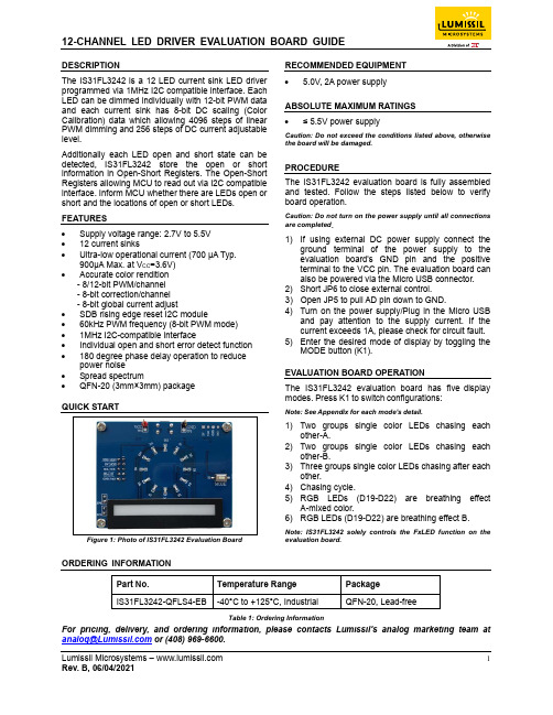
DESCRIPTIONThe IS31FL3242 is a 12 LED current sink LED driver programmed via 1MHz I2C compatible interface. Each LED can be dimmed individually with 12-bit PWM data and each current sink has 8-bit DC scaling (Color Calibration) data which allowing 4096 steps of linear PWM dimming and 256 steps of DC current adjustable level.Additionally each LED open and short state can bedetected, IS31FL3242 store the open orshortinformation in Open-Short Registers. The Open-Short Registers allowing MCU to read out via I2C compatible interface. Inform MCU whether there are LEDs open or short and the locations of open or short LEDs. FEATURES∙Supply voltage range: 2.7V to 5.5V∙12 current sinks∙Ultra-low operational current (700 µA Typ.900µA Max. at V CC=3.6V)∙Accurate color rendition- 8/12-bit PWM/channel- 8-bit correction/channel- 8-bit global current adjust∙SDB rising edge reset I2C module∙60kHz PWM frequency (8-bit PWM mode)∙1MHz I2C-compatible interface∙Individual open and short error detect function∙180 degree phase delay operation to reduce power noise∙Spread spectrum∙QFN-20 (3mm×3mm) packageQUICK STARTFigure 1: Photo of IS31FL3242 Evaluation Board RECOMMENDED EQUIPMENT∙ 5.0V, 2A power supplyABSOLUTE MAXIMUM RATINGS∙≤ 5.5V power supplyCaution: Do not exceed the conditions listed above, otherwise the board will be damaged.PROCEDUREThe IS31FL3242 evaluation board is fully assembled and tested. Follow the steps listed below to verify board operation.Caution: Do not turn on the power supply until all connections are completed.1) If using external DC power supply connect theground terminal of the power supply to the evaluation board's GND pin and the positive terminal to the VCC pin. The evaluation board can also be powered via the Micro USB connector.2) Short JP6 to close external control.3) Open JP5 to pull AD pin down to GND.4) Turn on the power supply/Plug in the Micro USBand pay attention to the supply current. If the current exceeds 1A, please check for circuit fault.5) Enter the desired mode of display by toggling theMODE button (K1).EVALUATION BOARD OPERATIONThe IS31FL3242 evaluation board has five display modes. Press K1 to switch configurations:Note: See Appendix for each mode’s detail.1) Two groups single color LEDs chasing eachother-A.2) Two groups single color LEDs chasing eachother-B.3) Three groups single color LEDs chasing after eachother.4) Chasing cycle.5) RGB LEDs (D19-D22) are breathing effectA-mixed color.6) RGB LEDs (D19-D22) are breathing effect B. Note: IS31FL3242 solely controls the FxLED function on the evaluation board.ORDERING INFORMATIONPart No. Temperature Range PackageIS31FL3242-QFLS4-EB -40°C to +125°C, Industrial QFN-20, Lead-freeTable 1: Ordering InformationFor pricing, delivery, and ordering information, please contacts Lumissil’s analog marketing team at *******************or (408) 969-6600.SOFTWARE SUPPORTJP6 (EXT CTRL) default setting is closed (jumper on). If it is open (when the EVB is powered on by 5V DC or micro-USB, no jumper JP6), the on-board MCU will configure its own I2C/SDB pins to High Impedance status so an external source can driver the I2C/SDB signals to control the IS31FL3242 LED driver, the on-board MCU will also configure the U4 to open the VLED (Single color LED+) and close the VRGB. When JP5 open, AD pin pulled down to GND by R13.Figure 2: Photo of Arduino UNO connected to EvaluationBoard The steps listed below are an example using the Arduino for external control.The Arduino hardware consists of an Atmel microcontroller with a bootloader allowing quick firmware updates. First download the latest Arduino Integrated Development Environment IDE (1.6.12 or greater) from /en/Main/Software. Also download the Wire.h library from /en/reference/wire and verify that pgmspace.h is in the directory …program Files(x86)/Arduino/hardware/tools/avr/avr/include/avr /. Then download the latest IS31FL3242 test firmware (sketch) from the Lumissil website /products/led-driver/fxled.1) Open JP5 and JP6.2) Connect the 5 pins from Arduino board toIS31FL3242 EVB:a) Arduino 5V pin to IS31FL3242 EVB VCC.b) Arduino GND to IS31FL3242 EVB GND.c) Arduino SDA (A4) to IS31FL3242 EVB SDA.d) Arduino SCL (A5) to IS31FL3242 EVB SCL.e) If Arduino use 3.3V MCU VCC, connect3.3V to IS31FL3242 EVB SDB, if Arduinouse 5.0V MCU VCC, connect 5.0V to EVBSDB.(Arduino UNO is 5.0V, so SDB=5.0V)3) Use the test code in appendix Ⅰor download thetest firmware (sketch) from the Lumissil website,a .txt file and copy the code to Arduino IDE,compile and upload to Arduino.4) Run the Arduino code and the initial mode willchange the Blue LED brightness every second.Note: the white color LEDs cannot be controlled when the onboard STM32F103C8T6 is disabled.(Some early board we provided is still controlling the single color LED, if want to switch between single color LED and RGB, remove the U4 and connect the VCC to the LED+)Please refer to the datasheet to get more information about IS31FL3242.GND SDBVCCFigure 3: IS31FL3242 Application SchematicBILL OF MATERIALSName Symbol Description Qty Supplier Part No.LED Driver U1 Matrix LED Driver 1 Lumissil IS31FL3242 MCU U2 Microcontroller 1 STM STM32F103C8T6 LDO U3 3.0V LDO 1 SGMICRO SGM2019-3.0YN5G PMOS U4 PMOS 1 ANPEC APM4953LED D1~D12 LED, SMD Blue 12 EVERLIGHT19-217/BHC-AN1P2/3TRGB LED D19~D22 RGB LED, SMD 4 EVERLIGHT 99-235/RSGBB7C-A22/2Dor99-235/RGBC/TR8Diode DS1 Diode, SMD 1 DIODES DFLS240 Crystal Y1 Crystal, 8MHz 1 HLX HC-49S Resistor R1,R3 RES,2k,1/10W,±5%,SMD 2 Yageo RC0603JR-072KLResistorR2,R4,R6,R7,R8RES,100k,1/10W,±5%,SMD 5 Yageo RC0603JR-07100KLResistor R9 RES,1k,1/10W,±5%,SMD 1 Yageo RC0603JR-071KL Resistor R10,R11 RES,22R,1/10W,±5%,SMD 2 Yageo RC0603JR-0722RL Resistor R12 RES,1.5k,1/10W,±5%,SMD 1 Yageo RC0603JR-071K5L Resistor R13 RES,10k,1/10W,±5%,SMD 1 Yageo RC0603JR-07100KLResistor R16,R19,R22,R25RES,20R,1/10W,±5%,SMD(Note 1)4 Yageo RC0603JR-0720RLResistor R15,R17,R18,R20,R21,R23,R24,R26RES,20R,1/10W,±5%,SMD 8 Yageo RC0603JR-0720RLCapacitor C1,C2,C9 CAP,100nF,16V,±20%,SMD 3 Yageo CC0603MRX7R7BB104 Capacitor C3 CAP,10µF,16V,±20%,SMD 1 Yageo CC0603MRX5R7BB106 Capacitor C4,C5 CAP, 1µF,16V,±10%,SMD 2 Yageo CC0603KRX7R7BB105 Capacitor C6 CAP,10nF,16V,±10%,SMD 1 Yageo CC0603KPX7R7BB103 Capacitor C7,C8 CAP,33pF,50V,±5%,SMD 2 Yageo CQ0603JRNPO9BN360 Button K1(Bottom) Button 1Micro USB CON1 Micro USB 1Bill of Materials, refer to Figure 3 above.Note 1: The value of these resistors on the evaluation board is 20Ω. For PV CC=5V and red LED application, prefer 51Ω for these resistors as shown in datasheet Figure 1.Figure 5: Board PCB Layout - Top LayerFigure 7: Board PCB Layout - Bottom LayerCopyright © 2021 Lumissil Microsystems. All rights reserved. Lumissil Microsystems reserves the right to make changes to this specification and its products at any time without notice. Lumissil Microsystems assumes no liability arising out of the application or use of any information, products or services described herein. Customers are advised to obtain the latest version of this device specification before relying on any published information and before placing orders for products.Lumissil Microsystems does not recommend the use of any of its products in life support applications where the failure or malfunction of the product can reasonably be expected to cause failure of the life support system or to significantly affect its safety or effectiveness. Products are not authorized for use in such applications unless Lumissil Microsystems receives written assurance to its satisfaction, that:a.) the risk of injury or damage has been minimized;b.) the user assume all such risks; andc.) potential liability of Lumissil Microsystems is adequately protected under the circumstancesREVISION HISTORYRevision Detail Information DateA Initial release 2020.11.30B Update the BOM 2021.06.04APPENDIX Ⅰ: IS31FL3242 Arduino Test Code V01A #include<Wire.h>#include<avr/pgmspace.h>#define Addr_GND 0x88int PWM_Gama64[128]={0x00,0x01,0x02,0x03,0x04,0x05,0x06,0x07,0x08,0x09,0x0b,0x0d,0x0f,0x11,0x13,0x16,0x1a,0x1c,0x1d,0x1f,0x22,0x25,0x28,0x2e,0x34,0x38,0x3c,0x40,0x44,0x48,0x4b,0x4f,0x55,0x5a,0x5f,0x64,0x69,0x6d,0x72,0x77,0x7d,0x80,0x88,0x8d,0x94,0x9a,0xa0,0xa7,0xac,0xb0,0xb9,0xbf,0xc6,0xcb,0xcf,0xd6,0xe1,0xe9,0xed,0xf1,0xf6,0xfa,0xfe,0xff,0xff,0xfe,0xfa,0xf6,0xf1,0xed,0xe9,0xe1,0xd6,0xcf,0xcb,0xc6,0xbf,0xb9,0xb0,0xac,0xa7,0xa0,0x9a,0x94,0x8d,0x88,0x80,0x7d,0x77,0x72,0x6d,0x69,0x64,0x5f,0x5a,0x55,0x4f,0x4b,0x48,0x44,0x40,0x3c,0x38,0x34,0x2e,0x28,0x25,0x22,0x1f,0x1d,0x1c,0x1a,0x16,0x13,0x11,0x0f,0x0d,0x0b,0x09,0x08,0x07,0x06,0x05,0x04,0x03,0x02,0x01,0x00};void setup() {// put your setup code here, to run once:Wire.begin();Wire.setClock(400000);//I2C 400kHz// pinMode(4,OUTPUT);//SDB// digitalWrite(4,HIGH);//SDB_HIGHInit_FL3242();}void loop() {// put your main code here, to run repeatedly://IS31FL3242_mode1();//8-bit modeIS31FL3242_mode2();//12-bit mode}void IS_IIC_WriteByte(uint8_t Dev_Add,uint8_t Reg_Add,uint8_t Reg_Dat) {Wire.beginTransmission(Dev_Add/2);Wire.write(Reg_Add); // sends regaddressWire.write(Reg_Dat); // sends regaddressWire.endTransmission(); // stop transmitting}void Init_FL3242(void){int i = 0;IS_IIC_WriteByte(Addr_GND,0x00,0x33);//Enable SSD 8-bit mode: 0x73 12-bit mode: 0x33 IS_IIC_WriteByte(Addr_GND,0x01,0x80);//GCCIS_IIC_WriteByte(Addr_GND,0x61,0x00);//frequency selectfor(i=0x0E;i<=0x25;i++){IS_IIC_WriteByte(Addr_GND,i,0x00);//PWM}for(i=0x02;i<=0x0D;i++){IS_IIC_WriteByte(Addr_GND,i,0xFF);//SL}}void IS31FL3242_mode1(void)// 8-bit mode{int i = 0;int j = 0;for (j=1;j<=127;j++)//all LED breath falling{for(i=0x0E;i<=0x24;i=i+2){IS_IIC_WriteByte(Addr_GND,i,PWM_Gama64[j]);//set all PWM}delay(20);//20ms}}void IS31FL3242_mode2(void)// 12-bit mode{int i, j,k,l;for(k=0;k<=0x0f;k++)//all LED breath rising{for(l=0x0F;l<=0x25;l=l+2){IS_IIC_WriteByte(Addr_GND,l,k);//set all PWM}for (j=0;j<=255;j++)//all LED breath falling{for(i=0x0E;i<=0x24;i=i+2){IS_IIC_WriteByte(Addr_GND,i,j);//set all PWM}delay(2);//2ms}}for(k=0x0f;k>=0;k--)//all LED breath falling{for(l=0x0F;l<=0x25;l=l+2){IS_IIC_WriteByte(Addr_GND,l,k);//set all PWM}for (j=255;j>=0;j--)//all LED breath falling{for(i=0x0E;i<=0x24;i=i+2){IS_IIC_WriteByte(Addr_GND,i,j);//set all PWM}delay(2);//2ms}}}。
飞利浦 BGA2716 数据手册

1.Product profile1.1General descriptionSilicon Monolithic Microwave Integrated Circuit (MMIC) wideband amplifier with internal matching circuit in a 6-pin SOT363 SMD plastic package.1.2Featuress Internally matched to 50Ωs Wide frequency range (3.2 GHz at 3 dB bandwidth)s Flat 23 dB gain (±1 dB up to 2.7 GHz)s 9 dBm output power at 1 dB compression point s Good linearity for low current (IP3out = 22 dBm)s Low second harmonic;−38 dBc at P L =−5 dBm sUnconditionally stable (K ≥ 1.2).1.3Applicationss LNB IF amplifiers s Cable systems s ISMsGeneral purpose.1.4Quick reference dataBGA2716MMIC wideband amplifierRev. 02 — 24 September 2004Product data sheetCAUTIONThis device is sensitive to electrostatic discharge (ESD). Therefore care should be taken during transport and handling.Table 1:Quick reference data Symbol Parameter ConditionsMin Typ Max Unit V S DC supply voltage -56V I S supply current -15.9-mA s 21 2insertion power gain f = 1 GHz -22.9-dB NF noise figuref = 1 GHz - 5.3-dB P L(sat)saturated load powerf = 1 GHz -11.6-dBm查询BGA2716供应商2.Pinning information3.Ordering information4.Marking5.Limiting valuesTable 2:PinningPin Description Simplified outlineSymbol1V S 2, 5GND23RF_OUT 4GND16RF_INSOT363132456sym052132, 564Table 3:Ordering informationType numberPackage NameDescriptionVersion BGA2716-plastic surface mounted package; 6 leadsSOT363Table 4:MarkingType numberMarking code BGA2716B7-Table 5:Limiting valuesIn accordance with the Absolute Maximum Rating System (IEC 60134).Symbol Parameter Conditions Min Max Unit V S DC supply voltage RF input AC coupled-6V I S supply current -30mA P tot total power dissipation T sp ≤ 90°C -200mW T stg storage temperature −65+150°C T j junction temperature -150°C P Dmaximum drive power-−10dBm6.Thermal characteristics7.CharacteristicsTable 6:Thermal characteristics Symbol ParameterConditions Typ Unit R th(j-sp)thermal resistance from junction to solder pointP tot = 200 mW;T sp ≤90°C300K/WTable 7:CharacteristicsV S =5V; I S =15.9mA; T j =25°C; measured on demo board; unless otherwise specified.Symbol Parameter ConditionsMin Typ Max Unit I S supply current1315.921mA s 21 2insertion power gain f = 100 MHz 2122.123dB f = 1 GHz2222.924dB f = 1.8 GHz 2223.125dB f = 2.2 GHz 2122.824dB f = 2.6 GHz 2022.124dB f = 3 GHz1920.822dB s 11 2input return losses f = 1 GHz 1517-dB f = 2.2 GHz 1012-dB s 22 2output return losses f = 1 GHz 1012-dB f = 2.2 GHz 911-dB s 12 2isolation f = 1.6 GHz 3031-dB f = 2.2 GHz 3335-dB NF noise figure f = 1 GHz - 5.3 5.4dB f = 2.2 GHz- 5.5 5.6dB B bandwidth at s 21 2−3 dB below flat gain at 1 GHz 3 3.2-GHzK stability factor f = 1 GHz - 1.4-f = 2.2 GHz - 1.9-P L(sat)saturated load power f = 1 GHz 1011.6-dBm f = 2.2 GHz67.5-dBm P L(1dB)load powerat 1dB gain compression;f = 1 GHz88.9-dBm at 1dB gain compression;f =2.2GHz5 6.1-dBm IM2second order intermodulation product at P L =−5 dBm;f 0=1GHz 3638-dBc IP3ininput, third order intercept pointf = 1 GHz −2−0.7-dBm f = 2.2 GHz −8−6.9-dBm IP3outoutput, third order intercept pointf = 1 GHz 2122.2-dBm f = 2.2 GHz 1515.9-dBm8.Application informationFigure 1 shows a typical application circuit for the BGA2716 MMIC. The device isinternally matched to 50Ω,and therefore does not need any external matching.The value of the input and output DC blocking capacitors C2and C3should not be more than 100pF for applications above 100 MHz. However, when the device is operated below 100 MHz,the capacitor value should be increased.The nominal value of the RF choke L1 is 100 nH. At the frequencies below 100 MHz this value should be increased. At frequencies above 1GHz, a lower value can be used to tune the output return loss. For optimal results, a good quality chip inductor or a wire-wound SMD type should be chosen.Both the RF choke and the 22nF supply decoupling capacitor C1 should be located as close as possible to the MMIC.The printed-circuit board (PCB)top ground plane,connected to pins 2,4and 5must be as close as possible to the MMIC, and ideally directly beneath it. When using via holes, use multiple via holes, located as close as possible to the MMIC.Figure 2 shows the PCB layout, used for the standard demonstration board.Fig 1.Typical application circuit.mgu436RF_OUTRF_IN C1L1C2C3GND2GND1V SV SRF inputRF output8.1Application examplesThe excellent wideband characteristics of the MMIC make it an ideal building block in IF amplifier such as LNBs (see Figure 3).Material = FR4; thickness = 0.6 mm,εr = 4.6.Fig 2.PCB layout and demonstration board showing components.001aab256OUTIN PHV +PHILIPSOUTIN PHV +PHILIPSC3C2L1C1DUT 30 mm30 mmAs second amplifier after an LNA, the MMIC offers an easy matching, low noise solution (see Figure 4).As driver amplifier in the TX path, the good linear performance and matched input/output offer quick design solutions (see Figure 5).Fig 3.Application as IF amplifier.Fig 4.Application as RF amplifier.Fig 5.Application as driver amplifier.fromRF circuitto IF circuit or demodulatormgu438mixeroscillatorwideband amplifierantennato IF circuit or demodulatormgu439mixerLNAoscillatorwideband amplifierfrom modulationor IF circuitto power amplifiermgu440mixeroscillatorwideband amplifierI S = 15.9 mA; V S = 5 V; P D =−35 dBm; Z o = 50Ω.Fig 6.Input reflection coefficient (s 11); typical values.I S = 15.9 mA; V S = 5 V; P D =−35 dBm; Z o = 50Ω.Fig 7.Output reflection coefficient (s 22); typical values.001aab25790°−90°50.50.2+0.2+2+5−5−2−0.2+0.5−0.5+1−121100.20.60.40.81.01.0−45°−135°45°135°180°0°4 GHz100 MHz001aab25890°−90°50.50.2+0.2+2+5−5−2−0.2+0.5−0.5+1−121100.20.60.40.81.01.0−45°−135°45°135°180°0°4 GHz 100 MHzI S = 15.9 mA; V S = 5 V; P D =−35dBm; Z o = 50Ω.P D =−35 dBm; Z o = 50Ω.(1)I S = 19.5 mA; V S = 5.5 V .(2)I S = 15.9 mA; V S = 5 V .(3)I S = 12.4 mA; V S = 4.5 V .Fig 8.Isolation ( s 12 2) as a function of frequency;typical values.Fig 9.Insertion gain ( s 21 2) as a function offrequency; typical values.f = 1 GHz; Z o = 50Ω.(1)V S = 5.5 V .(2)V S = 5 V .(3)V S = 4.5 V .f = 2.2 GHz; Z o = 50Ω.(1)V S = 5.5 V .(2)V S = 5 V .(3)V S = 4.5 V .Fig 10.Load power as a function of drive power at1GHz; typical values.Fig 11.Load power as a function of drive power at2.2GHz; typical values.f (MHz)04000300010002000001aab259−40−200|s 12|2(dB)−60f (MHz)04000300010002000001aab260102030|s 21|2(dB)(1)(2)(3)P D (dBm)−40−10−30−20001aab2610−101020P L (dBm)−20(1)(2)(3)P D (dBm)−40−10−30−20001aab262−101020P L (dBm)−20(1)(2)(3)Z o = 50Ω.(1)I S = 19.5 mA; V S = 5.5 V .(2)I S = 15.9 mA; V S = 5 V .(3)I S = 12.4 mA; V S = 4.5 V .I S = 15.9 mA; V S = 5 V; Z o = 50Ω.Fig 12.Noise figure as a function of frequency; typicalvalues.Fig 13.Stability factor as a function of frequency;typical values.f (MHz)02500200010001500500001aab2636578NF (dB)4(1)(2)(3)f (MHz)04000300010002000001aab26423145K 0Table 8:Scattering parametersV S = 5 V; I S = 15.9 mA; P D =−35 dBm; Z o = 50Ω; T amb = 25°C.f (MHz)s11s21s12s22K-factorMagnitude (ratio)Angle(deg)Magnitude(ratio)Angle(deg)Magnitude(ratio)Angle(deg)Magnitude(ratio)Angle(deg)1000.182562102.779412.6958113.486820.02947228.749550.3923991.48628 1.3 2000.12346587.5527413.13419−5.2729170.035438−2.2023610.26785162.37296 1.2 4000.10785558.5851313.47149−31.73770.035299−22.543010.22725224.6455 1.2 6000.11473140.1407113.57901−53.096310.033167−43.063530.227993−3.493572 1.3 8000.13017624.2855513.67457−73.606650.033194−59.635030.234967−31.11084 1.3 10000.1449849.65761613.91705−94.019730.029047−76.099720.239818−60.54722 1.4 12000.160922−7.51889214.10949−114.550.028188−88.340450.242141−91.56898 1.4 14000.179351−23.3598914.2808−135.31170.025188−101.27290.243087−124.5484 1.4 16000.20199−41.0134914.3825−156.70410.022257−110.33420.24499−158.6224 1.5 18000.218268−60.7129414.26935−178.38430.019611−121.01920.255598167.5983 1.7 20000.233965−81.4825414.0667160.15040.018087−127.67650.269829136.117 1.8 22000.242904−103.110913.83968138.23790.017203−137.82130.283613106.0987 1.9 24000.246576−125.5213.46447115.75940.016318−138.87170.2905877.95189 2.0 26000.249069−148.870712.7463893.386440.015514−147.66220.28150550.68612 2.2 28000.243665−172.64611.8755871.027920.014954−152.19880.2513524.40624 2.5 30000.233266163.903510.9404950.427220.015522−163.87180.211425−0.674037 2.7 32000.222055140.775410.0562630.759080.016261−170.56370.165534−23.9944 2.9 34000.207486117.05319.57635711.983150.016664−176.54070.118726−46.28101 3.0 36000.19165494.644319.199166−7.6776430.016982176.93850.083354−72.36691 3.2 38000.17578371.95518.912598−27.730980.017094165.82270.058549−109.9804 3.3 40000.16376849.894368.618058−48.908740.017414157.60950.055225−163.7132 3.39.Package outlineFig 14.Package outline; SOT363 (SC-88).REFERENCESOUTLINE VERSION EUROPEAN PROJECTIONISSUE DATE IECJEDECEIAJ SOT363SC-88w BM b pD e 1epin 1indexAA 1L pQdetail XH EE v M AA B y01 2 mmscalecX132456Plastic surface mounted package; 6 leadsSOT363UNIT A 1max b p c D E e 1H E L p Q y w v mm0.10.300.202.21.80.250.101.351.150.65e 1.32.22.00.20.10.2DIMENSIONS (mm are the original dimensions)0.450.150.250.15A 1.10.897-02-2810.Revision historyTable 9:Revision historyDocument ID Release date Data sheet status Change notice Doc. number Supersedes BGA2716_220040924Product data sheet-939775013292BGA2716_N_1 Modifications:•The format of this data sheet has been redesigned to comply with the new presentation andinformation standard of Philips SemiconductorsBGA2716_N_120040202Preliminary data sheet-9397 750 12827-11.Data sheet status[1]Please consult the most recently issued data sheet before initiating or completing a design.[2]The product status of the device(s) described in this data sheet may have changed since this data sheet was published. The latest information is available on the Internet at URL .[3]For data sheets describing multiple type numbers, the highest-level product status determines the data sheet status.12.DefinitionsShort-form specification —The data in a short-form specification is extracted from a full data sheet with the same type number and title. For detailed information see the relevant data sheet or data handbook.Limiting values definition — Limiting values given are in accordance with the Absolute Maximum Rating System (IEC 60134). Stress above one or more of the limiting values may cause permanent damage to the device.These are stress ratings only and operation of the device at these or at any other conditions above those given in the Characteristics sections of the specification is not implied. Exposure to limiting values for extended periods may affect device reliability.Application information — Applications that are described herein for any of these products are for illustrative purposes only. Philips Semiconductors make no representation or warranty that such applications will be suitable for the specified use without further testing or modification.13.DisclaimersLife support —These products are not designed for use in life support appliances, devices, or systems where malfunction of these products can reasonably be expected to result in personal injury. Philips Semiconductors customers using or selling these products for use in such applications do so at their own risk and agree to fully indemnify Philips Semiconductors for any damages resulting from such application.Right to make changes —Philips Semiconductors reserves the right to make changes in the products - including circuits, standard cells, and/or software - described or contained herein in order to improve design and/or performance. When the product is in full production (status ‘Production’),relevant changes will be communicated via a Customer Product/Process Change Notification (CPCN). Philips Semiconductors assumes noresponsibility or liability for the use of any of these products, conveys no license or title under any patent, copyright, or mask work right to theseproducts,and makes no representations or warranties that these products are free from patent,copyright,or mask work right infringement,unless otherwise specified.14.Contact informationFor additional information, please visit: For sales office addresses, send an email to:**********************************Level Data sheet status [1]Product status [2][3]DefinitionI Objective data Development This data sheet contains data from the objective specification for product development. Philips Semiconductors reserves the right to change the specification in any manner without notice.IIPreliminary dataQualificationThis data sheet contains data from the preliminary specification.Supplementary data will be published at a later date.Philips Semiconductors reserves the right to change the specification without notice,in order to improve the design and supply the best possible product.III Product data ProductionThis data sheet contains data from the product specification. Philips Semiconductors reserves the right to make changes at any time in order to improve the design,manufacturing and supply.Relevant changes will be communicated via a Customer Product/Process Change Notification (CPCN).15.Contents1Product profile. . . . . . . . . . . . . . . . . . . . . . . . . . 11.1General description. . . . . . . . . . . . . . . . . . . . . . 11.2Features . . . . . . . . . . . . . . . . . . . . . . . . . . . . . . 11.3Applications . . . . . . . . . . . . . . . . . . . . . . . . . . . 11.4Quick reference data. . . . . . . . . . . . . . . . . . . . . 12Pinning information. . . . . . . . . . . . . . . . . . . . . . 23Ordering information. . . . . . . . . . . . . . . . . . . . . 24Marking. . . . . . . . . . . . . . . . . . . . . . . . . . . . . . . . 25Limiting values. . . . . . . . . . . . . . . . . . . . . . . . . . 26Thermal characteristics. . . . . . . . . . . . . . . . . . . 37Characteristics. . . . . . . . . . . . . . . . . . . . . . . . . . 38Application information. . . . . . . . . . . . . . . . . . . 48.1Application examples . . . . . . . . . . . . . . . . . . . . 59Package outline . . . . . . . . . . . . . . . . . . . . . . . . 1110Revision history. . . . . . . . . . . . . . . . . . . . . . . . 1211Data sheet status. . . . . . . . . . . . . . . . . . . . . . . 1312Definitions . . . . . . . . . . . . . . . . . . . . . . . . . . . . 1313Disclaimers. . . . . . . . . . . . . . . . . . . . . . . . . . . . 1314Contact information . . . . . . . . . . . . . . . . . . . . 13© Koninklijke Philips Electronics N.V.2004All rights are reserved.Reproduction in whole or in part is prohibited without the priorwritten consent of the copyright owner.The information presented in this document doesnot form part of any quotation or contract,is believed to be accurate and reliable and maybe changed without notice.No liability will be accepted by the publisher for anyconsequence of its use.Publication thereof does not convey nor imply any license underpatent- or other industrial or intellectual property rights.Date of release: 24 September 2004Document number: 9397 750 13292。
ADP1612 ADP1613升压转换器评估板文档说明书

650 kHz/1.3 MHz Step-Up Converter Evaluation Board DocumentationEVAL-ADP1612/ADP1613Rev. AEvaluation boards are only intended for device evaluation and not for production purposes. Evaluation boards are supplied “as is” and without warranties of any kind, express, implied, or statutory including, but not limited to, any implied warranty of merchantability or fitness for a particular purpose. No license is granted by implication or otherwise under any patents or other intellectual property by application or use of evaluation boards. Information furnished by Analog Devices is believed to be accurate and reliable. However , no responsibility is assumed by Analog Devices for its use, nor for any infringements of patents or other rights of third parties that may result from its use. Analog Devices reserves the right to change devices or specifications at any time without notice. T rademarks and registered trademarks are the property of their respective owners. Evaluation boards are not authorized to be used in life support devices or systems.O ne Technology Way, P.O. Box 9106, Norwood, MA 02062-9106, U.S.A.Tel: 781.329.4700 Fax: 781.461.3113 ©2009–2010 Analog Devices, Inc. All rights reserved.FEATURESInput voltage range1.8 V to 5.5 V for the ADP1612-5-EVALZ2.5 V to 5.5 V for the ADP1613-12-EVALZ Output voltage5 V for ADP1612-5-EVALZ 12 V for ADP1613-12-EVALZShunt-selectable 1.3 MHz or 650 kHz switching frequency Jumper for enable/shutdown controlComponents optimized for the indicated output voltagesGENERAL DESCRIPTIONThe ADP1612/ADP1613 evaluation module is a complete step-up dc-to-dc switching converter application with components selected to allow operation over the full range of input and load conditions for the 5 V (ADP1612) and 12 V (ADP1613) output voltages. The evaluation boards can be adjusted for different output voltages by changing R1 and R2. In addition, L1, D1, C3, and R3 may need to be adjusted and should be recalculated to ensure stable operation. The ADP1612/ADP1613 evaluation module operates inpulse-width modulation (PWM) current mode with up to 94% efficiency. The shunt-selectable switching frequency and PWM current-mode architecture allow for excellent transient response, easy noise filtering, and the use of small, cost-saving external inductors and capacitors. Other key features include a 33 nF soft start capacitor, undervoltage lockout (UVLO), thermal shutdown (TSD), and jumper selected enable. The evaluation module demonstrates the operation and performance of the ADP1612/ADP1613.This data sheet includes I/O descriptions, setup instructions, the schematic, and the PCB layout drawings for the ADP1612/ ADP1613 step-up converter evaluation module. Use this data sheet in conjunction with the ADP1612/ADP1613 data sheet available on .TYPICAL APPLICATION CIRCUIT06772-002Figure 1. Step-Up Regulator ConfigurationEVAL-ADP1612/ADP1613Rev. A | Page 2 of 8TABLE OF CONTENTSFeatures .............................................................................................. 1 General Description ......................................................................... 1 Typical Application Circuit ............................................................. 1 Revision History ............................................................................... 2 Evaluation Board Hardware ............................................................ 3 Input/Output Connectors ........................................................... 3 Evaluation Setup ........................................................................... 3 Performance Evaluation .............................................................. 4 Evaluation Board Schematic and Layout .......................................5 Layout Guidelines..........................................................................5 Ordering Information .......................................................................6 Bill of Materials ..............................................................................6 Ordering Guide .............................................................................7 ESD Caution.. (7)REVISION HISTORY1/10—Rev. 0 to Rev. AChanges to Figure 4 to Figure 6 (3)12/09—Revision 0: Initial VersionEVAL-ADP1612/ADP1613Rev. A | Page 3 of 8EVALUATION BOARD HARDWAREThe ADP1612/ADP1613 evaluation module is fully assembled and tested. The following sections describe the various connec-tors on the board, the proper evaluation setup, and the testing capabilities of the evaluation module.INPUT/OUTPUT CONNECTORSEN Test BusThe EN connector is used to enable/disable the converter via the EN pin. Use one of the following methods to enable the converter. Do not leave the EN pin floating. •Use a jumper to connect the top two pins of the EN test bus. This connects EN to VIN and enables the converter (see Figure 2).08527-003PLACE JUMPER HEREFigure 2. Enabled Jumper Position•Use a jumper to connect the bottom two pins of the EN test bus. This connects EN to GND and disables the converter (see Figure 3).08527-004PLACE JUMPER HEREFigure 3. Disabled Jumper Position•Alternatively, connect a voltage between VIN and GND to the center pin of the EN test bus for independent control of the EN pin voltage (see Figure 4).08527-005CONNECT EXTERNALDEVICE HEREFigure 4. EN Pin Direct Connection0 Ω Shunt FREQ (R4)This shunt selects the switching frequency via the FREQ pin. Several methods are available as follows. •Shunt the top pads of FREQ (R4) for 1.3 MHz operation (see Figure 5).08527-006PLACE SHUNT HEREFigure 5. 1.3 MHz Operation Shunt Position•Shunt the bottom pads of FREQ (R4) for 650 kHz operation (see Figure 6).08527-007PLACE SHUNT HEREFigure 6. 650 kHz Operation Shunt Position• If this shunt is left open, the part defaults to 650 kHz.VOUT Test BusThe output voltage at the VOUT test bus is set by the resistive voltage divider network, R1 and R2. A load can be attached to the VOUT test bus.VIN Test BusThe VIN test bus connects the positive input supply voltage to the VIN pin. Connect the power supply to this bus and keep the wires as short as possible to minimize the EMI transmission.GND Test BusThe GND test bus is the power ground connection for the part via the GND pin as well as the bypass capacitors. Connect ground connections from external equipment to this bus.SW Test PointThe SW test point is for measuring the switch node (SW pin) behavior and switching frequency.EVALUATION SETUPFollow these setup instructions to ensure proper operation of the ADP1612/ADP1613 evaluation module:1. Select the passive components for the bypass capacitance,desired output voltage, compensation, and start-up time, using the applications information from the ADP1612/ ADP1613 data sheet.2. Connect the input supply ground to GND.3. Connect the positive input supply to VIN.4. Connect the desired load between VOUT and GND. Themaximum continuous output current of the ADP1612/ ADP1613 is dependent upon the input and output conditions.5. Apply a voltage between 1.8 V and 5.5 V (ADP1612) or2.5 V and 5.5 V (ADP1613) to the VIN test bus.6. Move the jumper on the EN test bus to the enabled position.EVAL-ADP1612/ADP1613Rev. A | Page 4 of 8PERFORMANCE EVALUATIONThe following sections discuss tests and the resulting oscil-loscope waveforms. Oscilloscope waveforms and typical performance characteristics are provided in the ADP1612/ ADP1613 data sheet.Line RegulationThe line regulation is observed and measured by monitoring the output voltage (VOUT) while varying the input voltage (VIN).Load RegulationThe load regulation is observed and measured by monitoring the output voltage (VOUT) while sweeping the applied load between VOUT and GND. To minimize voltage drop, use short low resistance wires, especially for heavy loads.EfficiencyThe efficiency, η, is measured by comparing the input power to the output powerININ OUT OUT I V I V ××=ηLine TransientThe line transient performance is evaluated by generating a high speed voltage transient on the input (VIN) and observing the behavior of the evaluation module at the inductor (SW) and the output (VOUT.)Load TransientThe load transient performance is evaluated by generating a fast current transient on the output (VOUT) and observing the behavior of the evaluation module at the inductor (SW) and the output (VOUT.)Oscillator FrequencyThe oscillator frequency can be measured by connecting an oscilloscope to the SW pin.Inductor CurrentThe inductor current is made accessible by removing one side of the inductor from its pad and connecting a current loop in series. Place an oscilloscope current probe on the loop to view the current waveform.EVAL-ADP1612/ADP1613Rev. A | Page 5 of 8EVALUATION BOARD SCHEMATIC AND LAYOUT08527-008Figure 7. ADP1612/ADP1613Boost Application Evaluation Board Schematic08527-00908527-01Figure 9. ADP1612/ADP1613 Boost Application PCB Bottom LayerLAYOUT GUIDELINESFor high efficiency, good regulation, and stability, a well-designed printed circuit board (PCB) layout is essential. Use the following guidelines when designing PCBs:•Keep the low ESR input capacitor, C IN (labeled as C7 in Figure 8), close to VIN and GND. This minimizes noise injected into the part from board parasitic inductance. •Keep the high current path from C IN (labeled as C7 in Figure 8) through the L1 inductor to SW and GND as short as possible.•Keep the high current path from VIN through L1, the rectifier (D1), and the output capacitor, C OUT (labeled as C4 in Figure 8), as short as possible.• Keep high current traces as short and as wide as possible. •Place the feedback resistors as close to FB as possible to prevent noise pickup. Connect the ground of the feedback network directly to an AGND plane to make a Kelvin connection to the GND pin.•Place the compensation components as close as possible to COMP . Connect the ground of the compensation network directly to an AGND plane that makes a Kelvin connection to the GND pin.•Connect the soft start capacitor, C SS (labeled as C1 in Figure 8), as close to the device as possible. Connect the ground of the soft start capacitor to an AGND plane that makes a Kelvin connection to the GND pin.•Avoid routing high impedance traces from the compensa-tion and feedback resistors near any node connected to SW or near the inductor to prevent radiated noise injection.EVAL-ADP1612/ADP1613Rev. A | Page 6 of 8ORDERING INFORMATIONBILL OF MATERIALSTable 1. ADP1612 (V OUT = 5 V)Qty Reference Designator Description Manufacturer 1 Part Number 1 U1 ADP1612 step-up converter Analog Devices, Inc. ADP1612 1 L1Inductor, 4.7 μH Coilcraft DO3316P-472ML 1 D1 Diode ON Semiconductor M BRS2040LT3 1 C1Soft start capacitor, MLCC, 33 nF, 50 V, 0805, ±10% Panasonic–ECG ECJ-2VB1H333K C2 Compensation capacitor Open 1 C3Compensation capacitor, 1200 pF, 50 V, 0805, ±10% Panasonic–ECG ECJ-2VB1H122K1 C4 Output capacitor, 10 µF, 25 V, 1206, ±10%Taiyo Yuden TMK316BJ106KL-T C5 Output capacitor Open C6 Output capacitor Open1 C7 Input capacitor, 10 μF, 16 V, 0805, ±10%Taiyo Yuden EMK212BJ106KG-T C8 Input capacitor Open C9 Input capacitor Open1 R1 Output voltage divider, 30.0 kΩ, 0805, ±1%Yageo RC0805FR-0730KL 1 R2 Output voltage divider, 10.0 kΩ, 0805, ±1% Vishay/Dale CRCW080510K0FKEA 1 R3 Compensation resistor, 12 kΩ, 0805, ±5% Yageo RC0805JR-0712KL 1 FREQ/R4 Frequency select shunt resistor, 0 Ω, 0805, 1.3 MHz (top 2 pads) Yageo RC0805JR-070RL 10 EN, VIN, SW,VOUT, GNDHeader (0.10”, single/double row, straight) Sullins Electronics PBC36SAAN1Equivalent substitutions may be made for all resistors and capacitors.Table 2. ADP1613 (V OUT = 12 V)Qty ReferenceDesignator Description Manufacturer 1 Part Number 1 U1 ADP1613 step-up converter Analog Devices, Inc. ADP1613 1 L1Inductor, 6.8 μH Coilcraft DO3316P-682ML 1 D1 Diode ON Semiconductor M BRA340T3G 1 C1Soft start capacitor, 33 nF, 50 V, 0805, ±10% Panasonic–ECG ECJ-2VB1H333K C2 Compensation capacitor Open 1 C3 Compensation capacitor, 1000 pF, 50 V, 0805, ±10% Panasonic–ECG ECJ-2VB1H102K 1 C4Output capacitor, 10 μF, 25 V, 1206, ±10% Taiyo Yuden TMK316BJ106KL-T C5 Output capacitor Open C6 Output capacitor Open 1 C7Input capacitor, 10 μF, 16 V, 0805, ±10% Taiyo Yuden EMK212BJ106KG-T C8 Input capacitor Open C9 Input capacitor Open 1 R1 Output voltage divider, 86.6 kΩ, 0805, ±1% Yageo RC0805FR-0786K6L 1 R2 Output voltage divider, 10.0 kΩ, 0805, ±1% Vishay/Dale CRCW080510K0FKEA 1 R3 Compensation resistor, 10 kΩ, 0805, ±5% Yageo RC0805JR-0710KL 1 FREQ/R4 Frequency select shunt resistor, 0 Ω, 0805, 1.3 MHz (top 2 pads) Yageo RC0805JR-070RL 10 EN, VIN, SW,VOUT, GNDHeader (0.10”, single/double row, straight) Sullins Electronics PBC36SAAN1Equivalent substitutions may be made for all resistors and capacitors.EVAL-ADP1612/ADP1613Rev. A | Page 7 of 8ORDERING GUIDEModel 1Description ADP1612-5-EVALZ ADP1612 Evaluation Board, 5 VOutput Voltage ConfigurationADP1612-BL1-EVZ ADP1612 Blank Evaluation Board ADP1613-12-EVALZ ADP1613 Evaluation Board,12 V Output Voltage ConfigurationADP1613-BL1-EVZ ADP1613 Blank Evaluation Board1Z = RoHS Compliant Part.ESD CAUTIONEVAL-ADP1612/ADP1613Rev. A | Page 8 of 8NOTES©2009–2010 Analog Devices, Inc. All rights reserved. Trademarks and registered trademarks are the property of their respective owners.EB08527-0-1/10(A)。
SGS-THOMSON M2716 数据手册

Figure 1. Logic DiagramM2716NMOS 16K (2K x 8) UV EPROM2048 x 8 ORGANIZATION525mW Max ACTIVE POWER, 132mW Max STANDBY POWER ACCESS TIME: –M2716-1 is 350ns –M2716 is 450nsSINGLE 5V SUPPLY VOLTAGE STATIC-NO CLOCKS REQUIREDINPUTS and OUTPUTS TTL COMPATIBLE DURING BOTH READ and PROGRAM MODESTHREE-STATE OUTPUT with TIED-OR-CAPABILITYEXTENDED TEMPERATURE RANGE PROGRAMMING VOLTAGE: 25V DESCRIPTIONThe M2716 is a 16,384 bit UV erasable and elec-trically programmable memory EPROM, ideally suited for applications where fast turn around and pattern experimentation are important require-ments.The M2716 is housed in a 24 pin Window Ceramic Frit-Seal Dual-in-Line package. The transparent lid allows the user to expose the chip to ultraviolet light to erase the bit pattern. A new pattern can then be written to the device by following the programmingprocedure.Table 1. Signal NamesJuly 19941/9查询M27128A-1F1供应商Figure 2. DIP Pin ConnectionsNote: Except for the rating "Operating Temperature Range", stresses above those listed in the T able "Absolute Maximum Ratings" may cause permanent damage to the device. These are stress ratings only and operation of the device at these or any other conditions above those indicated in the Operating sections of this specification is not implied. Exposure to Absolute Maximum Rating conditions for extended periods may affect device reliability. Refer also to the SGS-THOMSON SURE Program and other relevant quality documents.Table 2. Absolute Maximum RatingsDEVICE OPERATIONThe M2716 has 3 modes of operation in the normal system environment. These are shown in Table 3.Read Mode. The M2716 read operation requires that G = V IL , EP = V IL and that addresses A0-A10have been stabilized. Valid data will appear on the output pins after time t AVQV , t GLQV or t ELQV (see Switching Time Waveforms) depending on which is limiting.Deselect Mode . The M2716 is deselected by mak-ing G = V IH . This mode is independent of EP and the condition of the addresses. The outputs are Hi-Z when G = V IH . This allows tied-OR of 2 or more M2716’s for memory expansion.Standby Mode (Power Down). The M2716 may be powered down to the standby mode by making EP = V IH. This is independent of G and automat-ically puts the outputs in the Hi-Z state. The power is reduced to 25% (132 mW max) of the normal operating power. V CC and V PP must be maintained at 5V. Access time at power up remains either t AVQV or t ELQV (see Switching Time Waveforms).ProgrammingThe M2716 is shipped from SGS-THOMSON com-pletely erased. All bits will be at “1" level (output high) in this initial state and after any full erasure.Table 3 shows the 3 programming modes.Program Mode . The M2716 is programmed by introducing “0"s into the desired locations. This is done 8 bits (a byte) at a time. Any individual address,sequential addresses, or addresses chosen at ran-dom may be programmed. Any or all of the 8 bits associated with an address location may be pro-grammed with a single program pulse applied to the EP pin. All input voltage levels including the program pulse on chip enable are TTL compatible.The programming sequence is: with V PP = 25V, V CC = 5V, G = V IH and EP = V IL , an address is selected and the desired data word is applied to the output pins (V IL = “0" and V IH = ”1" for both address and data). After the address and data signals are stable the program pin is pulsed from V IL to V IH with apulse width between 45ms and 55ms. Multiple pulses are not needed but will not cause device damage. No pins should be left open. A high level (V IH or higher) must not be maintained longer than t PHPL (max) on the program pin during program-ming. M2716’s may be programmed in parallel in this mode.Program Verify Mode. The programming of the M2716 may be verified either one byte at a time during the programming (as shown in Figure 6) or by reading all of the bytes out at the end of the programming sequence. This can be done with V PP = 25V or 5V in either case. V PP must be at 5V for all operating modes and can be maintained at 25V for all programming modes.Program Inhibit Mode. The program inhibit mode allows several M2716’s to be programmed simul-taneously with different data for each one by con-trolling which ones receive the program pulse. All similar inputs of the M2716 may be paralleled. Pulsing the program pin(from V IL to V IH) will pro-gram a unit while inhibiting the program pulse to a unit will keep it from being programmed and keep-ing G = V IH will put its outputs in the Hi-Z state.ERASURE OPERATIONThe M2716 is erased by exposure to high intensity ultraviolet light through the transparent window. This exposure discharges the floating gate to its initial state through induced photo current. It is recommended that the M2716 be kept out of direct sunlight. The UV content of sunlight may cause a partial erasure of some bits in a relatively short period of time.An ultraviolet source of 2537 Å yielding a total integrated dosage of 15 watt-seconds/cm2 power rating is used. The M2716 to be erased should be placed 1 inch away from the lamp and no filters should be used.An erasure system should be calibrated peri-odically. The erasure time is increased by the square of the distance (if the distance is doubled the erasure time goes up by a factor of 4). Lamps lose intensity as they age, it is therefore important to periodically check that the UV system is in good order.This will ensure that the EPROMs are being com-pletely erased. Incomplete erasure will cause symptoms that can be misleading. Programmers, components, and system designs have been erro-neously suspected when incomplete erasure was the basic problem.DEVICE OPERATION (cont’d)Note: X = V IH or V IL.Table 3. Operating ModesFigure 3. AC Testing Input Output WaveformsInput Rise and Fall Times ≤ 20ns Input Pulse Voltages0.45V to 2.4V Input and Output Timing Ref. Voltages0.8V to 2.0VAC MEASUREMENT CONDITIONSFigure 4. AC Testing Load CircuitNote that Output Hi-Z is defined as the point where datais no longer driven.Note: 1. Sampled only, not 100% tested.Table 4. Capacitance (1) (T A = 25 °C, f = 1 MHz )Note: 1.V CC must be applied simultaneously with or before V PP and removed simultaneously or after V PP .Table 5. Read Mode DC Characteristics (1)(T A = 0 to 70 °C or –40 to 85 °C; V CC = 5V ± 5% or 5V ± 10%; V PP = V CC )Figure 5. Read Mode AC WaveformsNotes:1.V CC must be applied simultaneously with or before V PP and removed simultaneously or after V PP .2.Sampled only, not 100% tested.Table 6. Read Mode AC Characteristics (1)(T A = 0 to 70 °C or –40 to 85 °C; V CC = 5V ± 5% or 5V± 10%; V PP = V CC)Note: 1.V CC must be applied simultaneously with or before V PP and removed simultaneously or after V PP .Table 7. Programming Mode DC Characteristics (1)(T A = 25 °C; V CC = 5V ± 5%; V PP = 25V ± 1V)Notes:1.V CCmust be applied simultaneously with or before V PP and removed simultaneously or after VPP .2.Sampled only, not 100% tested.Table 8. Programming Mode AC Characteristics (1)(T A = 25 °C; V CC = 5V ± 5%; V PP = 25V ± 1V)Figure 6. Programming and Verify Modes AC Waveforms-1350 ns, 5V ±10%blank450 ns, 5V ±5%FFDIP24W10 to 70 °C 6–40 to 85 °CORDERING INFORMATION SCHEMEFor a list of available options (Speed, V CC Tolerance, Package, etc...) refer to the current Memory Shortform catalogue.For further information on any aspect of this device, please contact SGS-THOMSON Sales Office nearest to you.FDIP24WDrawing is not to scaleInformation furnished is believed to be accurate and reliable. However, SGS-THOMSON Microelectronics assumes no responsibility for the consequences of use of such information nor for any infringement of patents or other rights of third parties which may result from its use. No license is granted by implication or otherwise under any patent or patent rights of SGS-THOMSON Microelectronics. Specifications mentioned in this publication are subject to change without notice. This publication supersedes and replaces all information previously supplied. SGS-THOMSON Microelectronics products are not authorized for use as critical components in life support devices or systems without express written approval of SGS-THOMSON Microelectronics.© 1994 SGS-THOMSON Microelectronics - All Rights ReservedSGS-THOMSON Microelectronics GROUP OF COMPANIESAustralia - Brazil - China - France - Germany - Hong Kong - Italy - Japan - Korea - Malaysia - Malta - Morocco - The Netherlands - Singapore - Spain - Sweden - Switzerland - Taiwan - Thailand - United Kingdom - U.S.A.。
RT7276GQW 评估板用户指南说明书

EVB_RT7276GQWRT7276GQWEvaluation BoardPurposeThe RT7276 is a high-performance 700kHz 3A step down regulator with an internal power switch and synchronous rectifier. This document explains the function and use of the RT7276 evaluation board (EVB) and provides information to enable operation and modification of the evaluation board and circuit to suit individual requirements.Table of ContentsPurpose (1)Introduction (2)General Product Information (2)Key Performance Summary Table (3)Bench Test Setup Conditions (4)Headers Description and Placement (4)Test Points (5)Power-up & Measurement Procedure (5)Output Voltage Setting (5)Schematic, Bill of Materials and Board Layout (6)EVB Schematic Diagram (6)Bill of Materials (7)EVB Layout (8)Other Technical Information (11)Evaluation Board IntroductionGeneral Product InformationGeneral DescriptionThe RT7276 is a high-performance 700kHz 3A step down regulator with an internal power switch and synchronous rectifier. It features quick transient response using its Advanced Constant On-Time (ACOT TM) control architecture that provides stable operation with small ceramic output capacitors and without complicated external compensation, among other benefits. The input voltage range is from 4.5V to 18V and the output is adjustable from 0.765V to 8V. The proprietary ACOT TM control improves upon other fast response constant on-time architectures, achieving nearly constant switching frequency over line, load, and output voltage ranges. Since there is no internal clock, response to transients is nearly instantaneous and inductor current can ramp quickly to maintain output regulation without large bulk output capacitance. The RT7276 is stable with and optimized for ceramic output capacitors.With its internal 90mΩ switch and 60mΩ synchronous rectifier, the RT7276 displays excellent efficiency and good behavior across a range of applications, especially for low output voltages and low duty cycles. Cycle-by cycle current limit, input under-voltage lock-out, externally-adjustable soft-start, output under- and overvoltage protection, and thermal shutdown provide safe and smooth operation in all operating conditions.The RT7276 evaluation board uses the RT7276GQW IC in a WDFN-10L3x3 package with an exposed thermal pad. The IC is also available in a PTSSOP-14 package with an exposed thermal pad.Features●Fast Transient Response●Steady 700kHz Switching Frequency at PWM●3A Output Current●Advanced Constant On-Time (ACOT TM) Control●Optimized for Ceramic Output Capacitors● 4.5V to 18V Input Voltage Range●Internal 90mΩ Switch and 60mΩ Synchronous Rectifier●0.765V to 8V Adjustable Output Voltage●Externally-adjustable, Pre-biased Compatible Soft-Start●Cycle-by-Cycle Current Limit●Output Over- and Under-voltage Shut-downEvaluation BoardKey Performance Summary TableKey features Evaluation board number: PCB002_V1 Default Input voltage 12VMax Output Current 3ADefault Output Voltage 1.05VDefault Marking & Package Type RT7276GQW (WDFN-10L 3x3)Operation Frequency Steady 700kHz at PWMOther Key Features Advanced constant On-time(ACOT TM) controlPower GoodAdjustable Soft-start (external capacitor)PSM/ PWM Auto SwitchedProtection Over current protection:Cycle-by-Cycle Current LimitHiccup Mode Output Over- and Under-voltage Shut-downEvaluation Board Bench Test Setup ConditionsHeaders Description and PlacementPlease carefully inspect the EVB IC and external components, comparing them to thefollowing Bill of Materials, to ensure that all components are installed and undamaged. If anycomponents are missing or damaged during transportation, please contact the distributor or***********************************.Evaluation BoardTest PointsThe EVB is provided with the test points and pin names listed in the table below.Test point/Pin nameSignal Comment (expected waveforms or voltage levels on test points) VIN Input voltage Input voltage range = 4.5V to 18VVOUT Outputvoltage Default output voltage = 1.05VOutput voltage range = 0.765V to 8V(see ‘’ Output Voltage Setting’’ section for changing output voltage level) GND Ground Ground reference for the input voltage, output voltage and analog ground SW Switching node test point SW waveformEN Enable test point Enable signal. Drive EN or install a shorting block on Jumper JP1 toenable operation (shorting 2-3) or disable operation (shorting 1-2).JP1 Chip enable control Install jumper or drive EN directly to enable or disable operationBOOT Boot strap supply test point Floating supply voltage for the high-side N-MOSFET switchSS Soft-start control test point Soft start waveformPVCC Linear regulator output testpointInternal linear regulator output= 5.1VPG Power good output testpoint Connected to PVCC through R29, PG voltage is 5.1V when soft-start is complete and the output voltage is in regulationPower-up & Measurement Procedure1. Connect a jumper at JP1 terminals 1 and 2, connecting EN to GND, to disable operation.2. Apply a 12V nominal input power supply (4.5V < V IN < 18V) to the VIN and GND terminals.3. Set the jumper at JP1 to connect terminals 2 and 3, connecting EN to VIN through resistor R30, to enableoperation.4. Verify the output voltage (approximately 1.05V) between VOUT and GND.5. Connect an external load up to 3A to the VOUT and GND terminals and verify the output voltage and current.Output Voltage SettingSet the output voltage with the resistive divider (R23, R28) between VOUT and GND with the midpoint at FB. The output is set by the following formula:OUT R23V = 0.765 x (1 + )R28The installed V OUT capacitors (C11, C12) are 22μF, 16V X5R ceramic types. Do not exceed their operating voltage range and consider their voltage coefficient (capacitance vs. bias voltage) and ensure that the capacitance is sufficient to maintain stability and provide sufficient transient response for your application. Installing a small 5pF to 22pF capacitor at C30 (in parallel with R23) may be desirable to improve transient response for higher output voltages. See the RT7276 IC datasheet for more information.Evaluation BoardSchematic, Bill of Materials and Board LayoutEVB Schematic DiagramR2910k TP1PGTP2PVCCTP3ENTP4SSVIN TP5BOOTL2NFGNDU5WDFN-10L 3x3EN1FB2PVCC3SS4VIN10VIN 9BOOT 8SW7PG 5SW 6G N D11TP6JP1EN 123R30100kR2822kR238.2kC291uFC30NFL11.4uHVOUT GNDC270.1uFGP 3GP 2C710uF C80.1uFC910uFGP 4C100.1uFC1122uFC1222uFC283.9nFGND CP1Short GP 5GP1GNDC7, C9: 10μF/50V/X5R, 1206, TDK C3216X5R1H106K C11, C12: 22μF/16V/X5R, 1210, Murata GRM32ER61C226K L1: 1.4μH TAIYO YUDEN NR8040T1R4N, DCR=7m ΩEvaluation BoardBill of MaterialsReference QtyPart number Description Package Manufacture U51RT7276GQWDC/DC Converter WDFN-10L 3x3RichtekC7,C9 2 C3216X5R1H106K160AB 10μF/±10%/50V/X5R 1206 TDKCeramic Capacitor C11,C12 2 GRM32ER61C226KE20# 22μF/±10%/16V/X5R 1210 MurataCeramic Capacitor C28 1 0603B392K500 3.9nF/±10%/50V/X7R 0603 WALSINCeramic Capacitor C8,C10,C27 3 C1608X7R1H104K080AA 0.1μF/±10%/50V/X7R 0603 TDKCeramic CapacitorC29 1 C1608X5R1E105K080AC1μF/±10%/25V/X5R0603 TDK Ceramic Capacitor C30 0Not Installed 0603L1 1 NR8040T1R4N 1.4μH/7A/±30%, DCR=7m Ω, Inductor8mmx8mmx4mm TAIYO YUDENL2 0 Not Installed R28 1 22k/±5%, Resistor 0603 R23 1 8.2k/±5%, Resistor 0603 R29 1 10k/±5%, Resistor 0603 R30 1 100k/±5%, Resistor0603 CP1 1 0 (Short) JP1 1 3-Pin Header TP1/2/3/4/5/6 6Test Pin GP 5Golden PinEvaluation Board EVB LayoutTop View (1st layer)Bottom View (4th Layer)Evaluation BoardComponent Placement Guide—Component Side (1st layer)PCB Layout—Component Side (1st Layer)PCB Layout—Inner Side (2nd Layer)PCB Layout—Inner Side (3rd Layer)Component Placement Guide—Bottom Side (4th Layer)PCB Layout—Bottom Side (4th layer)Other Technical Information▪F or more information, please find the related datasheet or application notes from the Richtek website ▪ Please check ACOT TM landing page for other ACOT TM products and more technical documents./2013www/acottm.jspEVB_RT7276GQW。