verilog实验指导
verilog 实验实验一具体步骤
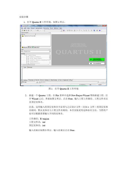
实验步骤1.打开Quartus II工作环境,如图1所示。
图1 打开Quartus II工作环境2.新建一个Quartus工程,在File菜单中选择New Project Wizard帮助新建工程。
打开Wizard之后,界面如图2所示。
点击Next,输入工程工作路径、工程文件名以及顶层实体名。
注意:这里输入的顶层实体名字必须与之后设计文件(比如.v文件)的顶层实体名相同,默认实体名与工程文件名相同,本次实验采用这种命名方法,当然用户也可以根据需要输入不同的实体名。
工作路径:E:\xinjian工程文件名:led顶层实体名:led输入结束后如图3所示。
输入结束后点击Next。
图2 New Project Wizard界面图3 输入设计工程信息3.添加设计文件,界面如图4所示。
如果用户之前已经有设计文件(比如.v文件),那么再次添加相应文件,如果没有完成的设计文件,点击Next,之后添加并且编辑设计文件。
图4 添加设计文件4.选择设计所用器件。
由于本次实验使用Altera公司提供的DE2开发板,用户必须选择与DE2开发板相对应的FPGA器件型号。
在Family菜单中选择CycloneII在Target device选项框中选择Specific device selected in ‘A vailable devices’ list 在A vailable device列表中选择EP2C35F672C6这个型号的器件。
完成后如图5所示,点击Next。
图5 选择相应器件5.设置EDA工具。
设计中可能会用到的EDA工具有综合工具、仿真工具以及时序分析工具。
在本次实验中不使用这些工具,因此点击Next直接跳过设置。
图6 设置EDA工具6.查看新建工程总结。
在基本设计完成后,Quartus II会自动生成一个总结让用户核对之前的设计(如图7所示),确认后点击Finish完成新建。
图7 新建工程总结在完成新建后,Quartus II界面中Project Navigator的Hierarchy标签栏中会出现用户正在设计的工程名以及所选用的器件型号,如图8所示。
Verilog HDL 实验报告

Verilog实验报告班级:学号:姓名:实验1 :用 Verilog HDL 程序实现直通线1 实验要求:(1) 编写一位直通线的 Veirlog HDL 程序.(2) 编写配套的测试基准.(3) 通过 QuartusII 编译下载到目标 FPGA器件中进行验证.(4) 建议用模式 52 试验程序:module wl(in,out);input in;output out;wire out;assign out=in;endmodule3 测试基准:`include “wl.v”module wl_tb;reg in_tb;wire out_tb;initialbeginin_tb =0;#100 in_tb =1;#130 in_tb =0;endendmodule4 仿真图形:实验2 :用 Verilog HDL 程序实现一位四选一多路选择器1实验要求:(1) 编写一位四选一多路选择器的 Veirlog HDL 程序.(2) 编写配套的测试基准.(3) 通过 QuartusII 编译下载到目标 FPGA器件中进行验证.(4)建议用模式 52 试验程序:module mux4_to_1 (out,i0,i1,i2,i3,s1,s0);output out;input i0,i1,i2,i3;input s1, s0;reg out;always @ (s1 or s0 or i0 or i1 or i2 or i3)begincase ({s1, s0})2'b00: out=i0;2'b01: out=i1;2'b10: out=i2;2'b11: out=i3;default: out=1'bx;endcaseendendmodule3 测试基准:`include "mux4_to_1.v"module mux4_to_1_tb1;reg ain,bin,cin,din;reg[1:0] select;reg clock;wire outw;initialbeginain=0;bin=0;cin=0;din=0;select=2'b00;clock=0;endalways #50 clock=~clock;always @(posedge clock)begin#1 ain={$random} %2;#3 bin={$random} %2;#5 cin={$random} %2;#7 din={$random} %2;endalways #1000 select[0]=!select[0];always #2000 select[1]=!select[1];mux4_to_1 m(.out(outw),.i0(ain),.i1(bin),.i2(cin),.i3(din),.s1(select[1]),.s0(select[0])); endmodule4 仿真图形:实验3:用 Verilog HDL 程序实现十进制计数器1实验要求:(1) 编写十进制计数器的 Veirlog HDL 程序. 有清零端与进位端, 进位端出在输出为 9 时为高电平.(2) 编写配套的测试基准.(3) 通过 QuartusII 编译下载到目标 FPGA器件中进行验证.(4) 自行选择合适的模式2 实验程序:module counter_10c (Q, clock, clear, ov);output [3:0] Q;output ov;input clock, clear;reg [3:0] Q;reg ov;initial Q=4'b0000;always @ (posedge clear or negedge clock)beginif (clear)Q<=4'b0;else if (Q==8)beginQ<=Q+1;ov<=1'b1;endelse if (Q==9)beginQ<=4'b0000;ov<=1'b0;endelsebeginQ<=Q+1;ov<=1'b0;endendendmodule3 测试基准:`include"./counter_10c.v"module counter_10c_tb;wire[3:0] D_out;reg clk,clr;wire c_out;reg[3:0] temp;initialbeginclk=0;clr=0;#100 clr=1;#20 clr=0;endalways #20 clk=~clk;counter_10c m_1(.Q(D_out),.clear(clr),.clock(clk),.ov(c_out)); endmodule4 仿真波形:实验4 :用 Verilog HDL 程序实现序列检测器1 实验要求:、(1) 编写序列检测器的 Veirlog HDL 程序. 检测串行输入的数据序列中是否有目标序列5'b10010, 检测到指定序列后, 用一个端口输出高电平表示.(2) 编写配套的测试基准.(3) 通过 QuartusII 编译下载到目标 FPGA器件中进行验证.(4) 自行选择合适的模式2试验程序:module e15d1_seqdet( x, z, clk, rst);input x,clk, rst;output z;reg [2:0] state;wire z;parameter IDLE = 3 'd0,A = 3'd1,B = 3'd2,C = 3'd3,D = 3'd4,E = 3'd5,F = 3'd6,G = 3'd7;assign z =(state==D && x==0)?1:0;always @(posedge clk or negedge rst)if(!rst)beginstate<=IDLE;endelsecasex(state)IDLE: if(x==1)state<=A;else state<=IDLE;A: if (x==0)state<=B;else state<=A;B: if (x==0)state<=C;else state<=F;C: if(x==1)state<=D;else state<=G;D: if(x==0)state<=E;else state<=A;E: if(x==0)state<=C;else state<=A;F: if(x==1)state<=A;else state<=B;G: if(x==1)state<=F;else state <=G;default: state<=IDLE;endcaseendmodule3测试基准:`include"e15d1_seqdet.v"`timescale 1ns/1ns`define halfperiod 20module e15d1_seqdet_tb;reg clk, rst;reg [23:0] data;wire z;reg x;initialbeginclk =0;rst =1;#2 rst =0;#30 rst =1;data= 20 'b1100_1001_0000_1001_0100;#(`halfperiod*1000) $stop;endalways #(`halfperiod) clk=~clk;always @ (posedge clk)begin#2 data={data[22:0],data[23]};x=data[23];ende15d1_seqdet m(.x(x),.z(z),.clk(clk),.rst(rst)); endmodule4仿真波形:。
verilog实验报告

verilog实验报告Verilog实验报告引言:Verilog是一种硬件描述语言(HDL),用于设计和模拟数字电路。
它是一种高级语言,能够描述电路的行为和结构,方便工程师进行数字电路设计和验证。
本实验报告将介绍我在学习Verilog过程中进行的实验内容和所获得的结果。
实验一:基本门电路设计在这个实验中,我使用Verilog设计了基本的逻辑门电路,包括与门、或门和非门。
通过使用Verilog的模块化设计,我能够轻松地创建和组合这些门电路,以实现更复杂的功能。
我首先创建了一个与门电路的模块,定义了输入和输出端口,并使用逻辑运算符和条件语句实现了与门的功能。
然后,我创建了一个测试模块,用于验证与门的正确性。
通过输入不同的组合,我能够验证与门的输出是否符合预期。
接下来,我按照同样的方法设计了或门和非门电路,并进行了相应的测试。
通过这个实验,我不仅学会了使用Verilog进行基本门电路的设计,还加深了对逻辑电路的理解。
实验二:时序电路设计在这个实验中,我学习了如何使用Verilog设计时序电路,例如寄存器和计数器。
时序电路是一种具有状态和时钟输入的电路,能够根据时钟信号的变化来改变其输出。
我首先设计了一个简单的寄存器模块,使用触发器和组合逻辑电路实现了数据的存储和传输功能。
然后,我创建了一个测试模块,用于验证寄存器的正确性。
通过输入不同的数据和时钟信号,我能够观察到寄存器的输出是否正确。
接下来,我设计了一个计数器模块,使用寄存器和加法电路实现了计数功能。
我还添加了一个复位输入,用于将计数器的值重置为初始状态。
通过测试模块,我能够验证计数器在不同的时钟周期内是否正确地进行计数。
通过这个实验,我不仅学会了使用Verilog设计时序电路,还加深了对触发器、寄存器和计数器的理解。
实验三:组合电路设计在这个实验中,我学习了如何使用Verilog设计组合电路,例如多路选择器和加法器。
组合电路是一种没有状态和时钟输入的电路,其输出只取决于当前的输入。
《FPGA设计与应用》实验指导书全(Verilog版)

《FPGA设计与应用》实验指导书熊利祥编武汉理工大学华夏学院2011年9月前言一、实验课目的数字电路与系统设计实验课是电子工程类专业教学中重要的实践环节,包括了ISE开发环境基本操作及FPGA的基本原理、基带传输系统的设计、Uart串口控制器电路的设计、PS/2接口的设计、VGA显示接口设计。
要求学生通过实验学会正确使用EDA技术,掌握FPGA器件的开发,熟练使用ISE开发环境,掌握Verilog语言的编程,掌握数字电路和系统的设计。
通过实验,使学生加深对课堂专业教学内容的理解,培养学生理论联系实际的能力,实事求是,严谨的科学作风,使学生通过实验结果,利用所学的理论去分析研究EDA技术。
培养学生使用Basys 2开发板的能力以及运用实验方法解决实际问题的能力。
二、实验要求:1.课前预习①认真阅读实验指导书,了解实验内容;②认真阅读有关实验的理论知识;③读懂程序代码。
2.实验过程①按时到达实验室;②认真听取老师对实验内容及实验要求的讲解;③认真进行实验的每一步,观察程序代码与仿真结果是否相符;④将实验过程中程序代码和仿真结果提交给老师审查;⑤做完实验后,整理实验设备,关闭实验开发板电源、电脑电源后方可离开。
3.实验报告①按要求认真填写实验报告书;②认真分析实验结果;③按时将实验报告交给老师批阅。
三、实验学生守则1.保持室内整洁,不准随地吐痰、不准乱丢杂物、不准大声喧哗、不准吸烟、不准吃东西;2.爱护公务,不得在实验桌及墙壁上书写刻画,不得擅自删除电脑里面的文件;3.安全用电,严禁触及任何带电体的裸露部分,严禁带电接线和拆线;4.任何规章或不按老师要求操作造成仪器设备损坏须论价赔偿。
目录实验一Uart通用串口接口的设计 (4)实验二PS/2接口的设计 (28)实验三VGA显示接口设计 (30)附录一 basys 2开发板资料 (36)实验一 Uart串口控制接口电路的设计一、实验目的1.掌握分频模块的设计方法。
天大Verilog实验说明书

试验一:开关、LED灯及多路复用器1.1将输入/输出器件连接到FPGA上实验原理:用18 个波段开关作为电路的输入,用18 个红色LED作为电路的输出,实现用波段开关控制红色LED,将开关拨到上方,相应的LED灯亮,否则LED灯灭实验步骤:实验步骤:(1)新建一个QuartusII工程(2)新建一个Verilog文件,将该Verilog文件添加到工程中并编译整个工程(3)分配引脚LEDR[0],PIN_AE23 SW[0],PIN_N25LEDR[1],PIN_AF23 SW[1],PIN_N26LEDR[2],PIN_AB21 SW[2],PIN_P25LEDR[3],PIN_AC22 SW[3],PIN_AE14LEDR[4],PIN_AD22 SW[4],PIN_AF14LEDR[5],PIN_AD23 SW[5],PIN_AD13LEDR[6],PIN_AD21 SW[6],PIN_AC13LEDR[7],PIN_AC21 SW[7],PIN_C13LEDR[8],PIN_AA14 SW[8],PIN_B13LEDR[9],PIN_Y13 SW[9],PIN_A13LEDR[10],PIN_AA13 SW[10],PIN_N1LEDR[11],PIN_AC14 SW[11],PIN_P1LEDR[12],PIN_AD15 SW[12],PIN_P2LEDR[13],PIN_AE15 SW[13],PIN_T7LEDR[14],PIN_AF13 SW[14],PIN_U3LEDR[15],PIN_AE13 SW[15],PIN_U4LEDR[16],PIN_AE12 SW[16],PIN_V1LEDR[17],PIN_AD12 SW[17],PIN_V2(4)编译该工程,完成后下载到FPGA中(5)通过拨动波段开关并观察红色LED的变化来验证所设计的功能是否正确参考代码:module led1(sw,d);input [17:0] sw;output [17:0] d;assign d=sw;endmodule1.2 3位宽5选1多路复用器实验原理:实现一个5选1的多路复用器,即从5个输入x,y,w,u,v中选取一个输出到m,输出选择用一个3位的输入s0s1s2实现实验步骤:(1)新建一个QuartusII工程(2)新建一个Verilog文件,用SW17~SW15作为选择端输入s0s1s2,用剩下的15个波段开关SW14~SW0作为u,v,w,x,y,用绿色LED即LEDG2~LEDG0作为输出M,将该Verilog 文件添加到工程中(3)分配连接波段开关、绿色LED的FPGA管脚LEDG[0],PIN_AE22LEDG[1],PIN_AF22LEDG[2],PIN_W19LEDG[3],PIN_V18LEDG[4],PIN_U18LEDG[5],PIN_U17LEDG[6],PIN_AA20LEDG[7],PIN_Y18(4)编译工程,完成后下载到FPGA中(5)拨动波段开关并观察绿色LED的变化,以验证3位5选1多路复用器的功能是否正确,确定从u到v的所有输入都能够被选择输出到M参考代码:module sel5to1(s,u,v,w,x,y,m);input[2:0] s,u,v,w,x,y;output[2:0] m;reg[2:0] m;always@(s)beginif(s=='b000)m=u;else if(s=='b001)m=v;else if(s=='b010)m=w;else if(s=='b011)m=x;else if(s=='b100)m=y;elsem=m;endendmodule1.3并行加法器实验原理:全加器的电路如图1(a)所示,输入为a,b和ci,输出为s和co,图1(b)是该电路的符号表示,表1为全加器的真值表,全加器实现了二进制加法,其输出为一个2位的二进制和co s=a+b+ci,用四个全加器模块的电路可以实现4位二进制数的加法,如图1(c)所示,这种加法器电路一般称为并行加法器(a ) (b )表1 实验步骤:(1)新建一个QuartusII 工程(2)建立一个Verilog 文件,然后用4个全加器电路来实现并行加法器电路(3)分别用SW7~SW4和SW3~SW0代表A 和B ,使用SW8代表加法器的进位输入cin ,而加法器的输出cout 和S 连接到LEDG4~LEDG0上,将代码添加到工程中 (4)进行引脚分配(5)改变输入A ,B 和cin 的值,观察计算结果是否正确 参考代码:module add(a,b,s,cout); input[3:0] a,b; output [3:0] s; output cout;wire c0,c1,c2;addone addone1(a[0],b[0],0,s[0],c0), addone2(a[1],b[1],c0,s[1],c1), addone3(a[2],b[2],c1,s[2],c2),addone4(a[3],b[3],c2,s[3],cout);endmoduleciabbcoF AFA FA FA FAs0s1s2s3c o c ic 1c 2c 3a1a2a3b1b2b3a0b0omodule addone(a,b,cin,s,cout);input a,b, cin;output s,cout;assign {cout,s}=a+b+cin;endmodule实验二:乘法器、锁存器及触发器2.1无符号乘法器实验原理:图1(a)位两位十进制数乘法的实现P=A*B,其它A=12,B=11,P=132,图1(b)是用4位二进制乘法实现的A和B的乘积,B的每一位要么是0,要么是1,因此算式中的加数要么是一位的A,要么是0000,图1(c)是用逻辑与实现的二进制乘法的过程12* 111212132(a)(b)图1(c)图2是实现4位二进制乘法P=A*B的电路,该电路中,用逻辑与实现每一行的乘法,用全加器实现每一列的加法,从而得到所需要的和。
EDA实验指导书Verilog版

实验一QUARTUSH的设计流程[输入方式:文本输入、图形输入、波形输入等]一、实验目的:1掌握QUARTU1S安装过程;2、熟悉QUARTU1S设计环境;3、掌握QUARTU1的设计过程。
二、实验内容:用文本输入法设计一个半加器。
三、实验步骤:一、安装QUARTUS II。
注:第一次安装QUARTU要安装license。
二、Q UARTU1设计开发步骤(一)、创建工作文件夹在windows中建立一个文件夹(又称工作库或WORK LIBRARY ),用于保存设计工程项目的有关文件。
注:设计工程项目的有关文件不能保存在根目录下,必须保存在一个文件夹之下。
例如建立的文件夹:E: \HADD(二)、启动Quartus II点击QUARTUS 9.0图标打开QUARTUS 9.0设计窗口。
(三)、设计文件输入1打开输入文件编辑器点击菜单File\new…新建立一个文本设计文件。
用文本输入法输入程序。
程序见附录。
2、保存文件,文件名名同实体名。
后缀.v(四)、全编译(逻辑综合)1创建工程点击菜单File'New Project Wizard ............... •进行工程设置。
完成工作文件夹的选定、工程名、顶层设计文件名、编程器件的确定等工程。
2、编译前的相关设置设置⑴选择PLD芯片:Assignmenmts'Settings'Device 弹出的窗口中选择选择芯片。
⑵选择配置芯片的工作方式:Assignmenmts'Settings\Device\Device&Pin Options 弹出的窗口中首选General 项,在Options 栏中选择Auto-restart-configuration after error.⑶选择配置芯片和编程方式:Assignmenmts\Settings\Device\Device&Pin Options弹出的窗口中选择Configuration 栏,在窗口中设置配置方式,配置芯片和是否生成压缩的配置文件。
Verilog实验指导书(2)
实验二:存储器的设计在计算机系统中,一般都提供一定数量的存储器。
在用FPGA实现的系统中,除可以使用FPGA本身提供的存储器资源外,还可以使用FPGA的外部扩充存储器。
本实验要求设计一个32×8 RAM,如下图所示,它包含5位地址、8位数据口和一个写控制端口。
实现这个存储器有两种方法:一种是采用FPGA上的存储器块实现。
EP2C35 FPGA片内共有105个M4K RAM块,每个M4K包含4096位,支持4K×1、2K×2、1K×4和512×8四种配置。
本实验选择512×8配置,而且只使用RAM中的32个字节。
另一种是采用外部存储器芯片实现。
每个M4K都有专用的寄存器用于所有输入、输出与时钟同步,因此在使用M4K时,要让输入、输出端口之一或全部与输入时钟同步。
改进之后的32×8 RAM 模块如下图所示。
1.用LPM实现32×8 RAM常用的逻辑电路如加法器、计数器、寄存器和存储器都可调用QuartusII提供的参数化功能模块LPM实现。
本实验采用LPM altsyncram实现存储器。
第1步:新建一个Quartus项目,并命名为lpm_sram。
第2步:新建一个图形文件,新建一个图形文件,并命名为lpm_sram.bdf。
打开符号(symbol)库,如下图所示。
从左边符号库中选中”altsyncram”,点击“ok”出现如下图所示的界面,第4步:点击Next按钮,在下一个对话框中选择“with one read/write port”模式,如下图所示。
第5步:点击Next按钮,在下一个对话框中选择存储器容量是32个字节,如下图所示。
第6步:其他对话框均采用默认值即可,最后按Finish按钮即完成RAM模块的设计。
第8步:添加相应的输入和输出端口,端口命名如下图所示。
第9步:进行语法检查,检查通过后,打开Pin Planner,用SW7~SW0作为数据输入、SW12~SW8作为地址的输入、SW13作为Write信号、结果显示在LEDG 上。
verilog hdl实验报告
verilog hdl实验报告《Verilog HDL实验报告》Verilog HDL(硬件描述语言)是一种用于描述电子系统的硬件的语言,它被广泛应用于数字电路设计和硬件描述。
本实验报告将介绍Verilog HDL的基本概念和使用方法,并通过实验展示其在数字电路设计中的应用。
实验目的:1. 了解Verilog HDL的基本语法和结构2. 掌握Verilog HDL的模块化设计方法3. 熟悉Verilog HDL的仿真和综合工具的使用实验内容:1. Verilog HDL的基本语法和结构Verilog HDL是一种硬件描述语言,其语法和结构类似于C语言。
它包括模块定义、端口声明、信号赋值等基本元素。
在本实验中,我们将学习如何定义Verilog模块,并使用端口声明和信号赋值描述数字电路的行为。
2. Verilog HDL的模块化设计方法Verilog HDL支持模块化设计,可以将复杂的电路分解为多个模块,每个模块描述一个子电路的行为。
在本实验中,我们将学习如何设计和实现Verilog模块,并将多个模块组合成一个完整的数字电路。
3. Verilog HDL的仿真和综合工具的使用Verilog HDL可以通过仿真工具进行功能验证,也可以通过综合工具生成实际的硬件电路。
在本实验中,我们将使用Verilog仿真工具对设计的数字电路进行功能验证,并使用综合工具生成对应的硬件电路。
实验步骤:1. 学习Verilog HDL的基本语法和结构2. 设计一个简单的数字电路,并实现Verilog模块描述其行为3. 使用仿真工具对设计的数字电路进行功能验证4. 使用综合工具生成对应的硬件电路实验结果:通过本实验,我们学习了Verilog HDL的基本概念和使用方法,并成功设计和实现了一个简单的数字电路。
我们使用仿真工具对设计的数字电路进行了功能验证,并使用综合工具生成了对应的硬件电路。
实验结果表明,Verilog HDL在数字电路设计中具有重要的应用价值。
Verilog HDL基础实验指南说明书
Using Fundamental Gates LabOverview:In this lab you will learn how to model simple gates using Verilog HDL and use them to create a more complex design. You will use fundamental gates using language supported primitive gates. After building the basic models you will create a hierarchical design. Outcome:You will understand how to use Verilog primitive gates. You will learn how to create a model using ISE Create Project wizard. You will instantiate lower-level models to create a bigger model. You will use ISE simulator to simulate the design. You will add user constraint file (ucf) to assign pins so the design can be targeted to National Instruments (NI) Digital Electronics FPGA Board. You will implement the design and create a bitstream file using ISE’s implementation tools. Once bitstream is created, you will download using ISE’s iMPACT program and verify the design functionality. Background:Verilog HDL is a hardware description language that can be used to model a digital system at many levels of abstraction ranging from algorithmic- to the gate- to the switch-level. The complexity of the digital system being modeled could vary from a simple gate to a complete system. Various levels of abstractions can be used in modeling the digital system based on its functionality and complexity. The language supports constructs and means to model the digital system in a hierarchical fashion. It also allows designer to describe timing explicitly. The richness of the language constructs is exploited by using same language constructs to test the system.A system- from a simple gate to a complex circuit- typically will have some input signals and some output signals to interact with either other digital devices or external board, and will have some functionality for which it has been designed. The basic unit of description in Verilog is the module. A module describes the functionality of a design and also describes the ports through which it communicates. The basic syntax of the module is:module module_name (port_list);DeclarationsStatementsendmoduleThe Verilog language is case sensitive. In the above example module and endmodule are keywords describing beginning of a module definition and ending of the module definition. You can not have nested module definitions, i.e. you can not have another module keyword within a module-endmodule pair. In the language, a statement is delimited by a semicolon. You can have multiple statements on a given line. The declarations in the above example can be definition of data types such as wire and reg, can be parameter definition, ports direction, functions, and tasks to name few. The Statements can be initial, always, and continuous assignment statements as well as module, gate, UDP (User Defined Primitives) instantiations. The Statements describe theactual functionality of the module. The identifiers must be defined using Declarations before they ca be used.The language defines three fundamental modeling styles. In a given module all or subset of these styles can be used. The three modeling styles are: Structural, Dataflow, and Behavioral. This lab exercise uses Structural style modeling. Structure can be described in Verilog using Built-in gate primitives, Switch-level primitives, User-Defined Primitives (UDP), and module instances. The Switch-level primitives are used to model fundamental gate functionality or a system built with switches or transistors. The UDP are used to define a unit as a black-box with providing functionality in truth-table form and explicit timing relationships between input and output ports. In this lab exercise you will use gate primitives and module instantiations. The language defines the following gates:[Verilog Quick Reference]Here is an example of instantiating a nor gate:nor X1 (S1, A, B);where X1 is the instance name. It is optional for the gate- or switch-level instantiation. The instance name is required for a module instantiation. S1 is output, and A and B are input.References:1. National Instruments’ Digital Electronics FPGA Board user manual2. Verilog HDL booksStephen Brown, Zvonko G. Vranesic, “Fundamentals of Digital Logic with Verilog Design”, 2002 Zainalabedin Navabi, “Verilog Digital Systems Design: RT Level Synthesis, Testbench, andVerification”, 2005Samir Paltinkar, “Verilog HDL: A Guide to Digital Design and Synthesis”, 2003Joseph Cavanagh, “Verilog HDL: Digital Design and Modeling”, 2007Michael D. Ciletti, “Modeling, Synthesis, and Rapid Prototyping with Verilog HDL”, 2003Douglas J. Smith, “HDL Chip Design: A Practical Guide for Designing, Synthesizing and Simulating ASICs and FPGAs using VHDL or Verilog”, 19963. On-line references:Verilog HDL Reference Card: /class/ee183/handouts_win2003/VerilogQuickRef.pdfVerilog Quick Reference: /~howard/pulsenet/docs/verilog_quikref.pdfTutorial on Verilog: .sa/COE/abouh/COE%20202%20Verilog%20Guidelines.pdfProblem Statement:Design a minority gate that has three inputs and one output. The output is logic 1 whenever the numbers of inputs which are logic 1 are zero or less than half of the input (i.e. 1 in this case).Implementation:The circuit to be designed consists of three inputs and one output. Typically such circuit can be implemented using a combinational network. A truth table is created and then some Boolean minimization technique (e.g. K-Map) may be used to reduce the number of logic gates used. The truth table for the design at hand is shown next along with K-Map and minimized Boolean expression.Inputs A B C OutputF0 0 0 1 0 0 1 1 0 1 0 10 1 1 01 0 0 1 1 0 1 0 1 1 0 0 1 1 1 01 1 0 11 0 0 000 01 11 1001AB C F = A C + B C + A B F = (A+C) * (B+C) * (A+B)The two expressions are equivalent. We will use the 2nd expression in this design.Procedure:1. Create a ISE project• Launch ISE: Select Start → Programs → Xilinx ISE Design Suite 10.1 →ISE → Project Navigator• In the Project Navigator, select File → New Project. The New Project Wizard opens• For Project Location, use the “…” button to browse to C:\NI\Verilog_labs, and then click OK• For Project Name, type minoritygate_lab • Click Next • Select the following options and click Next Device Family: Spartan3E Device: xc3s500E Package: ft256 Speed Grade: –5 Synthesis Tool: XST (VHDL/Verilog) Simulator: ISE Simulator (VHDL/Verilog)Preferred Language: Verilog•The Create New Source dialog will appear. You can use this dialog to createa new HDL source file by defining the module name and ports. You will dothis once to get experience. Subsequent files creation will be done using a text file rather than using the dialog. Click New Source button• A new source wizard will appear. Select Verilog Module as a source type andenter my_2or in the File name field and click Next• A Define Module form will appear. Enter in1, in2 as the input in Port Nam e field and out1 as the output. Change the input Direction to output by clicking and drop-down button and selection output as the direction. Click Next and then OK to create the file•Click Next and Add Existing Sources form will be displayed. Click Finish as we do not have anything to add•Click Finish. A project will be created and my_or2.v file be created and added to the project. The file will be opened and displayed in the editorwindow. You can enter related information regarding project name, target devices, etc. You will also see a module and endmodule statements arecreated. The only thing that is needed is to add the functionalityYou will notice that the project hierarchy view window showing the part information as well as my_2or as the top-level model•Enter a gate-level instantiation statement that uses primitive gate to perform or function on the two inputs and output the result with 2 ns delay•Save and close the file•Click New button () and select text file and click OK•Enter the module, endmodule, and gate-level instantiation statement to model 2-input and function using the port names as in1, in2, and out1•Save and close the file, giving my_2and.v as the filename•Similarly, create a new model for the minority gate functionality (3 inputs [in1, in2, and in3] and one output [out1]), instantiating my_2or and my_2and models, and using necessary number of fundamental gates instantiations and having 2 ns as the delay. Use named-mapped port convention. The named-port convention requires a port name of the parent module be listed firstpreceded with “.” followed by a net name that is connecting that port in the current module. In the below figure, .in1 is the port name of my_or2 mdoule (parent module) where as in1_n is the net name connecting to that port. In named-port mapping convention, one need not mention all the ports of the parent module. The unlisted parent module ports are drive logic 0 if theyinput and left unconnected if they are output.•Right-click on my_2or entry in the Sources window and select Add Source …•Select minoritygate.v and my_2and.v files and click Open•Click OK to finish the addition2. Simulate the design using ISIM•Right-click on the minoritygate entry in Sources window and select New Source•Select Test Bench Waveform as the source type and enter minoritygate_tb in the File name field. Click Next•Select minoritygate as the UUT to associate the testbench to the source model and click Next followed by clicking Finish button•Select combinatorial (internal clock) and click Finish to display the input and output signals. Click appropriately in the waveform window to generate input stimulus as shown below•Save the file•Select Sources tab and then click minoritygate in Sources window, and click on the drop-down button of the Sources for window and select Behavioral Simulation•Select minoritygate_tb in Sources tab, expand its entry to see UUT. Select Processes tab, expand Xilinx USE Simulator, and double-click on Simulate Behavioral Model entry to run the simulator•The source files will be compiled and the executable file(minoritygate_tb_ism_beh.exe) be generated which is then run, displaying the result in a waveform window•You can view lower-level signals by selecting Sim Insulator tab in Sources window, expanding hierarchy, selecting a particular instance, then clicking Sim Objects in tab in Processes window, and then selecting and dragging a desired signal(s) in the waveform window•You can zoom-in or zoom-out the waveform window by clicking on appropriate buttons ()•You can restart by clicking on () button and re-run by clicking on run for the specified time()button•You can change the run-time by typing in the new time field(), clicking restart button, and then clicking on run for the specified time button•Close the simulator by closing the waveform window and click OK to close the active simulator3. Implement the design•Select implementation in Sources for window•Select minoritygate module in Sources window•Expand User Constraints processes in Processes window•Double-click on Floorplan IO Pre-Synthesis to open PACE program•Click OK and then Yes to add ucf file•In PACE window assign pin locations and I/O Std as shown below•Click Save button• A dialog box will appear. Choose XST Default: <> option and click OK as we are using XST synthesis tools•Close the PACE program using File→Close• A minoritygate.ucf file will be added to the project. Open that file and see how the constraints are written•Close the file•Select minoritygate in Sources window and double-click on Implement Design process in Processes window. This will go through Synthesis, and Implementation stages•Expand Synthesis processes and double click on View RTL Schematic and View Technology Schematic processes to get different views•You can push-in to a lower-level schematic by double-clicking on the top-level•When the implementation is completed, expand Implement Design process to view the Place & Route report•Double-click on the Place & Route Report to view the report. Look at the resource utilization and note that 1 slice is being used•You can see similar information by clicking on Design Summary tab and looking at the various information4. Verify the design in hardware•Select minoritygate in Sources window and double-click on GenerateProgramming File process to generate the bit file for the designConfiguration Project (iMPACT) process•Connect the board with the USB-JTAG cable•Power ON the board•Click Finish to use the JTAG chain•Select minoritygate.bit file to be assigned to xc3s500e device and click Open•Click Bypass button for xcf04s and then OK to use FPGA device programming•Right-click on the FPGA and select Program•This will program the FPGA and DONE light will lit on the board•Once programmed successfully, verify the functionality by using SW0 thru SW2 and monitoring LD0 output. Verify that when more than one switch isturned ON, LD0 turns OFF•Once confirmed the functionality, power down the board and close ISE saving project changesConclusion:In this lab exercise you learned how to design a hierarchical system. You also learned how to model a circuit using gate-level as well as module-instantiations. You were able to simulate the design at each level and then verify the complete design in hardware board.。
Verilog_实验指导书
目录实验一简单组合逻辑电路的设计 0实验二简单时序逻辑电路的设计 (1)modelsim6.0使用教程 (2)实验一简单组合逻辑电路的设计一实验要求1.用verilog HDL语言描写出简单的一位数据比较器及其测试程序;2.用测试程序对比较器进行波形仿真测试;画出仿真波形;3. 总结实验步骤和实验结果。
二实验原理与内容这是一个可综合的数据比较器,很容易看出它的功能是比较数据a与数据b,如果两个数据相同,则给出结果1,否则给出结果0。
在Verilog HDL中,描述组合逻辑时常使用assign结构。
注意equal=(a==b)?1:0,这是一种在组合逻辑实现分支判断时常使用的格式。
模块源代码://--------------- compare.v -----------------module compare(equal,a,b);input a,b;output equal;assign equal=(a==b)?1:0; //a等于b时,equal输出为1;a不等于b时,//equal输出为0。
endmodule测试模块用于检测模块设计得正确与否,它给出模块的输入信号,观察模块的内部信号和输出信号,如果发现结果与预期的有所偏差,则要对设计模块进行修改。
测试模块源代码:`timescale 1ns/1ns //定义时间单位。
module comparetest;reg a,b;wire equal;initial //initial常用于仿真时信号的给出。
begina=0;b=0;#100 a=0; b=1;#100 a=1; b=1;#100 a=1; b=0;#100 $stop; //系统任务,暂停仿真以便观察仿真波形。
endcompare compare1(.equal(equal),.a(a),.b(b)); //调用模块。
endmodule实验二简单时序逻辑电路的设计一实验要求1.用verilog HDL语言描写出简单的二分之一分频器及其测试程序;2.用测试程序对分频器进行波形仿真测试;画出仿真波形;3.总结实验步骤和实验结果。
- 1、下载文档前请自行甄别文档内容的完整性,平台不提供额外的编辑、内容补充、找答案等附加服务。
- 2、"仅部分预览"的文档,不可在线预览部分如存在完整性等问题,可反馈申请退款(可完整预览的文档不适用该条件!)。
- 3、如文档侵犯您的权益,请联系客服反馈,我们会尽快为您处理(人工客服工作时间:9:00-18:30)。
一、ISE软件的基本介绍1、ISE用户界面ISE的界面如图1-1所示,由上到下主要分为标题栏、菜单栏、工具栏、工程管理区、源文件编辑区、过程管理区、信息显示区、状态栏等8部分。
标题栏:主要显示当前工程的名称和当前打开的文件名称。
菜单栏:主要包括文件(File)、编辑(Edit)、视图(View)、工程(Project)、源文件(Source)、操作(Process)、窗口(Window)和帮助(Help)等8个下拉菜单。
其使用方法和常用的Windows软件类似。
工具栏:主要包含了常用命令的快捷按钮。
灵活运用工具栏可以极大地方便用户在ISE中的操作。
在工程管理中,此工具栏的运用极为频繁。
工程管理区:提供了工程以及其相关文件的显示和管理功能,主要包括源文件视图(Source View),快照视图(Snapshot View)和库视图(Library View)。
其中源文件视图比较常用,显示了源文件的层次关系。
快照是当前工程的备份,设计人员可以随时备份,也可以将当前工程随时恢复到某个备份状态。
快照视图用于查看当前工程的快照。
执行快照功能的方法是选择菜单项Project | Take Snapshot。
库视图则显示了工程中用户产生的库的内容。
源文件编辑区:源文件编辑区提供了源代码的编辑功能。
过程管理区:本窗口显示的内容取决于工程管理区中所选定的文件。
相关操作和FPGA设计流程紧密相关,包括设计输入、综合、仿真、实现和生成配置文件等。
对某个文件进行了相应的处理后,在处理步骤的前面会出现一个图标来表示该步骤的状态。
信息显示区:显示ISE中的处理信息,如操作步骤信息、警告信息和错误信息等。
信息显示区的下脚有两个标签,分别对应控制台信息区(Console)和文件查找区(Find in Files)。
如果设计出现了警告和错误,双击信息显示区的警告和错误标志,就能自动切换到源代码出错的地方。
状态栏:显示相关命令和操作的信息。
2.ISE菜单的基本操作ISE所有的操作都可通过菜单完成,下面简要介绍ISE的菜单命令以及功能。
(1)File菜单File菜单的命令包括:New Project、Open Project、Open Examples、Close Project、Save Project As、New、Open、Save、Save As、Save All、Print Preview、Print、Recent Files、Recent Projects以及Exit等。
New Project命令:用于新建工程,是开始设计的第一步。
ISE会为新建的工程创建一个和工程同名的文件夹,专门用于存放工程的所有文件。
Open Project命令:用于打开已有的ISE工程。
高版本的ISE可以打开低版本的工程,但需要版本转换,该转换是单向的、不可逆的,因此需要做好版本备份。
低版本的ISE不能打开高版本的ISE工程。
Open Examples命令:用于打开ISE提供的各种类型的示例。
Close Project命令:关闭当前工程。
如果关闭前未保存文件,ISE会提示用户保存后再退出。
Save Project As命令:可将整个工程另存为其他名字的工程,在大型开发中,常使用该命令来完成版本备份。
New命令:用于新建源文件,可生成原理图、符号以及文本文件。
文本文件另存为时可修改其后缀名,以生成.v或.vhd的源文件。
Open命令:用于打开所有Xilinx所支持的文件格式,便于用户查看各类文件资源。
Save、Save As以及Save All命令:分别用于保存当前源文件、另存为当前源文件以及保存所有源文件。
用户要在开发当中养成及时保存文件的习惯,避免代码丢失。
Print Preview命令:用于打印预览当前文件,Print用于打印当前文件。
Recent Files命令:用于查看最近打开的文件。
Recent Projects命令:用于查看最近打开的工程。
Exit命令:用于退出ISE软件。
(2)Edit菜单Edit菜单的命令包括:Undo、Redo、Cut、Copy、Paste、Delete、Find、Find Next、Find in Files、Language Templates、Select All、Unselect All、Message Filters、Object Properties以及Preference等,大多数命令用于源代码开发中。
Undo命令:用于撤销当前操作,返回到前一状态。
Redo命令:是Undo命令的逆操作,用于恢复被撤销的操作。
Cut命令:剪贴选中的代码, 快捷键为“CRTL+X”。
Copy命令:复制选中的代码, 快捷键为“CRTL+C”。
Paste命令:粘贴剪贴和复制的代码, 快捷键为“CRTL+V”。
Delete命令:删除选中的代码。
Find命令:查找选中的文字,或寻找在其输入框中输入的内容,快捷键为“CRTL+F”。
Find Next命令:寻找下一个要查找的内容,并跳至相应的位置,快捷键为“F3 ”。
Language Templates命令:可打开语言模版,里面有丰富的学习资料,是非常完整的HDL语言帮助手册,其地位类似于VisualC++的MSDN。
Select All命令:选中所有的代码,其快捷键为“CRTL+A”。
Unselect All命令:撤销已选中的全部代码,是Select All的逆操作。
Message Filter命令:过滤消息,只显示用户期望的消息。
Preference命令:用于设定ISE的启动参数以及运行参数,有着众多的设置项,最常用的就是第三方EDA软件的关联设置,将在第4.5节详细介绍。
(2)View菜单View菜单主要管理ISE软件的视图,不涉及FPGA开发中的任何环节,其中常用的命令有Layout Horizontally、Layout Vertically以及Restore Default Layout。
Layout Horizontally命令:将水平地排列ISE主界面中过程管理区、过程管理区以及代码编辑区等主要栏目。
Layout Vertically命令:将垂直地排列ISE主界面中过程管理区、过程管理区以及代码编辑区等主要栏目。
Restore Default Layout命令:将恢复ISE默认的主界面布局。
(3)Project菜单Project菜单包含了对工程的各个操作,是设计中最常用的菜单之一,包括New Source、Add Source、Add Copy of source、Cleanup Project Files、Toggle Paths、Archive、Take Snapshot、Make Snapshot Current、Apply Project Properties以及Source Control命令。
New Source命令:用于向工程中添加源代码,可以添加HDL源文件、IP Core以及管脚和时序约束文件。
Add Source命令:将已有的各类源代码文件加入到工程中,Verilog模块的后缀为.v,VHDL模块的后缀为.vhd,IP core源文件为.xco文件或.xaw文件,约束文件的后缀为.ucf。
Add Copy of source命令,将目标文件拷贝一份添加到工程中。
Cleanup Project Files命令:用于清空综合和实现过程所产生的文件和目录。
如果在EDIF设计模式中,只清空实现过程所产生的文件。
Toggle Paths命令:用于显示或隐藏非工程文件夹中的远端源文件的路径;Archive命令:用于压缩当前工程,包括所有的文件,默认压缩类型为.zip格式。
Take Snapshot命令:用于产生一个工程快照,即当前目录和远程资源的一个只读记录,常用于版本控制。
Make Snapshot Current命令:用户恢复快照覆盖当前工程。
由于该命令会将当前工程删除,所以使用前一定要做好数据备份工作。
Apply Project Properties命令:应用工程属性,会提示用于选择相应工程。
Source Control常用于代码的导入和导出,有Export和Import两个子命令。
(4)Source菜单Source菜单主要面向工程管理区,包含了对资源文件的各个操作,每个命令的操作也都可以在工程管理区单击右键弹出的对话框中点击实现,包括:Open、Set as Top Module、Use SmartGuide、New Partition、Delete Partition、Partition properties、Partition Force、Remove、Move to library以及Properties等命令。
Open命令:可打开所有类型的源文件,包括.v、.vhd、.xco、.xaw以及.ucf等格式。
Set as Top Module命令:用于将选中的文件设置成顶层模块。
只有设置成顶层模块,才能对其综合、实现以及生成相应的二进制比特流文件。
Use SmartGuide命令:允许用户在本次实现时利用上一次实现的结果,包括时序约束以及布局布线结果,可节省实现的时间,但前提是工程改动不大。
New Partition命令:新建分区,常用于区域约束。
Delete Partition命令:删除区域约束的分区Partition properties命令:可设置分区属性,详细说明刻参考4.4.4节内容。
Partition Force命令:包含“Force Synthesis Out-of-data”和“Force Implement Design Out-of-data”两个指令,分别用于分区综合和增量设计。
Remove命令:把选中的文件从工程中删除,但仍保留在计算机硬盘上。
Move to library命令:将选中的源文件移动到相应的库中,以便建立用户文件库。
Properties命令:查看源文件属性,有Synthesis/Implementation Only、Simulation Only以及Synthesis/Imp+ Simulation三种类型,其中Simulation Only类文件只能仿真,不能被综合。
(5)Process菜单Process菜单包含了工程管理区的所有操作,每个命令的操作也都可以在过程管理区点击相应的图标实现,包括:Inmolement Top Module、Run、Rerun、Rerun All、Stop、Open Without Updating 以及Properties等命令。
Inmolement Top Module命令:完成顶层模块的实现过程。
Run命令:在工程过程栏,选中不同的操作,点击改命令,可分别启动综合、转换、映射、布局布线等过程。