Thin Film Process Introduction
薄膜技术英文课件:1introduction

Thin film
ρb≤ρtf(有问题)
Mb≤Mtf
small(um )
Large(mm)
17
2. Thin film vs. block material-1
Density Melting point Crystalline size
Bolck
Thin film
ρb≤ρtf(有问题)
Mb≤Mtf
39
Chemical vapor deposition(CVD)
• Thermal decomposition • Reaction on surface of substrate
The process of chemically reacting a volatile compound of a material to be deposited, with other gases, to produce a nonvolatile solid that deposits atomistically on a suitably placed substrate.
• GaN 、GaAs/GaAlAs、a-Si/a-SiC
– Thin film resistor(电阻), thin film capacitor(电容)
electroluminescence
• Ni-Cr low resistance thin film resistor
– Thin-film solar cell
– Piezoelectric(1.压电的) thin film for wave filtering
• ZnO 、AlN
– Sensitive thin fi2
• Optical thin film薄膜
FLX-2320 S Thin Film Stress Measurement Operation
FLX-2320 S Thin Film Stress MeasurementOperation ManualFor issues related to this instrument, please contact Ling Xie by phone 6-9069 (office) and 617-780-1821 (cell) or email ************1IntroductionThe FLX-2320-S determines stress by measuring the curvature change of pre- andpost- film deposition. The stress calculation is based on Stoney’s equation, whichrelates the biaxial modulus of the substrate, thickness of the film and the substrate,and the curvature change. The stress measurements can be made from -65ºC to 500ºC at a heating rate up to 30ºC/min. Stress variation with temperature can be used tocharacterize film properties such as moisture concentration, phase changes, thermalexpansion, volume changes, and plastic deformations.Other characteristics of the instrument include:•Dual wavelengths•Calculation of biaxial modules of elasticity, linear expansioncoefficient, stress uniformity and file subtraction•Calculation of water diffusion coefficient•2-D and 3-D view of wafer topography•Wafer size: 75 - 200 mm•Measurement temperature: from -65ºC to 500ºC•PC based controller•Speed: 5 seconds for 150 mm wafer•Minimum scan step: 0.02 mm•Maximum points per scan: 12502.Operating Safety•Laser: The FLX-2320 contains two 4 mW solid-state lasers with wavelengths of 670 nm and 780 nm. There is a shutter that will automatically block the laser beamwhen the chamber door is opened for loading and unloading a wafer. Therefore,there will be no reflected laser from sample.•High and Low Temperatures: Do not open the instrument door or touch any inside components, or the sample, until the temperature reading on the front panelreaches room temperature.3.Starting-Up Instrument3.1.Fill in log book first3.2.Turn on the Main Power switch3.3.Turn on the Laser3.4.If using Stress-Temperature mode, turn on the Heater and the Fan3.5.If using Stress-Temperature mode, open the inert and N2 gas valves on the gasmanifold.3.6.If using Stress-Temperature mode and the designed temperature is lower thanroom temperature, open the LN2 tank and the LN2 valve.ing Wafer Locator Rings4.1. A wafer locator ring is used to position the wafer at the center of the samplestage.4.2.Available ring sizes: 3”, 4”, 5”, and 6”; 8” wafers fit directly into the plate.4.3.The locator ring is marked at 30º intervals and has a notch at each 15 º interval.4.4.By rotating the ring and wafer, stress mapping across a whole wafer can beperformed.5.Performing Measurements5.1.Setting up a Process Program5.1.1.From Edit menu, choose Process Program5.1.2.In the Process Program dialog box, select the desired parameters(referencing followings)Field DescriptionMaximum Scan Points a maximum of 1250 points per scan can be usedbut 50 points are sufficient for an accuratemeasurement. Also only 50 data points are savedwith each scan to save space on the hard disk.Low Intensity Alarm Specify an intensity limit below whichmeasurement points will be ignored; 0.2 isrecommended.Elastic Modulus The biaxial elastic modulus of the substrateHole Diameter The diameter of the center region of the substrateto be skipped.Laser Selection Use the drop-down list to select Automatic, 670nm or 780 nm.5.2.First Stress Measurement – measure the stress before film deposition5.3. Single Stress Measurement5.3.1.Enter the same filename as in the First Stress Measurement5.3.2.Enter the same ID as entered in the First Measurement5.4. Stress-Time Measurement5.4.1. A total number of records in a data file are limited to 1000.5.4.2.Enter the same filename as in the First Measurement.5.4.3.Enter the same ID as entered in the First Measurement5.4.4.Enter the Time Interval the wafer will be measured.5.4.5.Enter the total time the wafer will be measured.5.5. Stress-Temperature Measurement5.5.1.Be sure the Heater and Fan on5.5.2.Be sure the inert and N2 gas lines are opened5.5.3.For low temperature measurement, open the LN2 tank and the valve onthe cooling line.5.5.4.For the Temperature Measurement, the glass piece and the hot plate covermust be put on the wafer stage to create a controlled measurementenvironment.5.5.5.Create a recipe5.5.5.1. Enter desired target temperature5.5.5.2. Enter a total time to reach the target temperature or enter a ramp speed.5.5.5.3.Enter a number of scans to be taken.5.5.5.4.Select the next recipe line and enter values. You can enter a maximumof 150 recipe lines and the total number of readings should not exceed1000.5.5.6. After finish the measurement, unload the wafer until room temperature.6.Creating and Displaying Graphs6.1.Creating Graphs6.1.1.Display a data file in the Data Editor window6.1.2.Choose Create from the Graph menu6.1.3.Enter desired parameters6.1.4. Choose the Create Graph button, the graph for the selected file isdisplayed.6.1.5.To display a graph of only some records, select the block of records, thenchoose Create Graph.6.2.Creating a Trend Plot6.2.1.Display a data file in the Data Editor window6.2.2.Choose Trend Plot from the Graph menu in the Data Editor window6.2.3.Enter desired parameters using following references:Field DescriptionUpper SL The Upper Specification Limit in stressLower SL The Lower Specification Limit in stressCalculate STD Y calculates the standarddeviation; the specification limits will not bedisplayed.6.2.4. Choose Trend Plot from the Trend Plot dialog.7.Data Analysis7.1.Diffusion CoefficientNote: The diffusion coefficient graphs only can be calculated from Stress-Timegraphs.7.1.1.To calculate the diffusion coefficient and plot it in a Graph window,choose Diffusion Coefficient from the Analysis menu7.1.2.Select the desired filename7.1.3.Select two points on the graph by double-clicking on the points.7.1.4. A plot of Diffusion Coefficient vs. Time will be displayed.7.2.Materials DatabaseUse the Materials Database option in the Edit menu to display a list ofavailable elastic & expansion coefficients.7.3.Elastic and Expansion Coefficient CalculationNote: Elastic and Expansion Coefficient only can be calculated from Stress-Temperature graphs.e the Stress-Temperature mode to run two temperature cycles on twodifferent substrates with the same film. For best results, use slow heating orcooling (<5ºC/min) to minimize the lag of wafer temperature behind theheating stage.7.3.2.Choose Elastic & Expansion from the Analysis menu7.3.3.Enter the film names7.3.4.Click on two points to plot and display the expansion coefficient.7.3.5.The average values of the expansion coefficient and the biaxial modulusdisplay in a dialog box.7.4.Thermal StressNote: Use the Thermal Stress option to display the thermal stresssuperimposed on the stress-temperature measurement data.7.4.1.Choose Thermal Stress from the Analysis menu7.4.2.Enter the file name7.4.3.Enter the temperature range7.5.Displaying Deflection MapsNote: Use the Deflection Maps to display 3-D view of the deflection. By takingseveral measurements at different angles you can display a complete 3-D mapof deflection over the wafer surface. The deflection can be plotted as thedifference of two groups of measurements (before- and after- a film deposition)or as an absolute deflection of a single measurement.7.5.1.Measure the wafer at different angles using a wafer locator ring.7.5.2.The IDs for each measurement in a group should be identical and in theformat xxxx-###, where XXX is any character (including spaces) and ###is the angular orientation. For example, the IDs for wafer T12 measuredevery 15º would be as follows:T12 - 0 T12 – 60 T12 –120T12 – 15 T12 – 75 T12 -135T12 – 30 T12 – 90 T12 -150T12 – 45 T12 -105 T12 -1657.5.3.When comparing two scans (before and after deposition), the first four IDcharacters must be identical for both scans and the orientation steps usedmust also be the same. Also, the dash must be in the fifth column and the### portion must be right justified.7.5.4.Choose 3DPlotting from the Analysis menu.7.5.5.To change the viewing angle, use the following key combinations:Key Combination DescriptionincrementF7 30ºCTRL + F7 Face on viewincrement10ºALT+F7incrementF8 30ºCTRL + F8 Face on viewincrementALT+F810ºincrementF9 45ºCTRL + F9 90º incrementincrement15ºALT+F9incrementF10 45ºCTRL + F10 90º incrementincrementALT+F10 15ºF11 Compress the view vertically by 50%F12 Stretch the view vertically by 50%8.Shutting-Down the Instrument8.1.Wait for the sample stage to reach room temperature.8.2.Close all open windows and choose Exit from the Measure menu.8.3.Exit from the Program Manager File menu.8.4.Turn off: Laser, Heater, Fan, and Main Power.8.5.Close the inert and N2 gas valves.8.6.Close the LN2 tank and the valve.plete log book.9.Revision HistoryRevision # Date Authors Changes/AdditionsissueXie InitialL.1.0 12/04/2007RevisedMartinE.2.0 4/28/2008RevisedMartinE.2.1 6/16/2008End of Document。
先进陶瓷材料 英语
Advanced Ceramic Materials: Innovations and Applications**Introduction:**Advanced ceramic materials represent a fascinating frontier in materials science and engineering. These materials, known for their exceptional properties, have found applications in a wide range of industries, from electronics and energy to aerospace and healthcare. This article explores the unique characteristics of advanced ceramics, their manufacturing processes, and their diverse applications across various sectors.**I. Characteristics of Advanced Ceramic Materials:**1. **High Hardness and Strength:**Advanced ceramics exhibit remarkable hardness and strength properties, making them suitable for applications where traditional materials may fail. Materials like silicon carbide and boron nitride are known for their exceptional hardness.2. **Low Thermal Conductivity:**Many advanced ceramics possess low thermal conductivity, making them useful for applications requiring thermal insulation. This property is vital in fields such as aerospace, where ceramic tiles are used to protect spacecraft from the intense heat during re-entry.3. **Electrical Insulation:**Ceramics are excellent electrical insulators, making them essential in electronics and telecommunications. Components like ceramic capacitors and insulating substrates play a crucial role in modern electronic devices.4. **Chemical Inertness:**Advanced ceramics often demonstrate high chemical inertness, resisting corrosion and degradation in harsh environments. This property makes them ideal for applications in chemical processing and biomedical devices.5. **Biocompatibility:**Some ceramics, such as alumina and zirconia, exhibit biocompatibility, making them suitable for use in medical implants. Their inert nature reduces the risk of adverse reactions within the human body.**II. Manufacturing Processes for Advanced Ceramics:**1. **Powder Processing:**The majority of advanced ceramics are produced through powder processing techniques. This involves the synthesis of ceramic powders, followed by shaping and sintering to achieve the desired final product.2. **Chemical Vapor Deposition (CVD):**CVD is a technique where ceramic materials are deposited onto a substrate from gaseous precursors. This process allows for the precise control of thin-film coatings and the production of intricate shapes.3. **Additive Manufacturing:**Recent advancements in additive manufacturing, or 3D printing, have extended to ceramics. This method enables the fabrication of complex ceramic structures with enhanced design flexibility.4. **Hot Isostatic Pressing (HIP):**HIP is a technique used to improve the density and mechanical properties of ceramics by subjecting them to high pressures and temperatures. This process reduces porosity and enhances material performance.**III. Applications of Advanced Ceramic Materials:**1. **Electronics and Semiconductors:**Ceramics such as alumina and silicon nitride are widely used in electronic components, including insulating substrates, capacitors, and semiconductor packages.2. **Aerospace Industry:**The aerospace sector utilizes ceramics for applications such as thermal protection systems on spacecraft, turbine blades in jet engines, and lightweight structural components.3. **Medical Implants:**Biocompatible ceramics like zirconia and alumina are employed in medical implants such as dental prosthetics and artificial joints, owing to their durability and compatibility with the human body.4. **Energy Sector:**Ceramics play a critical role in the energy industry, particularly in high-temperature environments. They are used in components for gas turbines, nuclear reactors, and solid oxide fuel cells.5. **Automotive Applications:**Advanced ceramics find use in the automotive sector for components that require high wear resistance and thermal stability, including brake components and engine components.**IV. Challenges and Future Prospects:**1. **Brittleness:**Despite their exceptional properties, ceramics are inherently brittle, limiting their use in certain applications. Ongoing research focuses on developing strategies to enhance the toughness of ceramics.2. **Cost and Manufacturing Complexity:**The production of advanced ceramics can be cost-intensive, and certain manufacturing processes involve complex procedures. Advancements in cost-effective manufacturing techniques are essential for widespread adoption.3. **Innovations in Composite Materials:**Researchers are exploring the incorporation of ceramics into composite materials to harness their unique properties while addressing limitations such as brittleness.4. **Nanotechnology Integration:**The integration of nanotechnology into ceramic materials is an area of active research. Nanoceramics exhibit enhanced properties, and their precise control at the nanoscale opens new possibilities for applications.**Conclusion:**Advanced ceramic materials stand at the forefront of materials innovation, offering a diverse range of properties that make them indispensable across various industries. As research continues to push the boundaries of ceramic science, addressing challenges and unlocking new potentials, these materials will likely play an increasingly pivotal role in shaping the technologies of the future. The versatility, durability, and unique characteristics of advanced ceramics position them as key contributors to advancements in electronics, healthcare, aerospace, and beyond.。
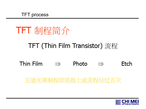
TFT制程简介
Resist stripping
Etching Process 1.AEI 2.CD measurement 3.Etch rate monitor 4.AOI
DRYP : PSC Dry etch (干式蚀刻)
STRP : Stripper (光阻去除)
何谓 TFT
TFT (thin film transistor)
薄膜晶体管 作为光线的开关 (控制液 晶分子的转动) Unit-Pixel 电路模型
T TF
各 Layer Total厚度约14500Å (1.45x10⁻⁵ mm): GLASS 厚度 0.7mm ≈ 1:5000
47“ TOP MON:450A A1:2500A BOTTOM MON:250A TOP MON:450A A1:2000A BOTTOM MON:250A
M2沉积
A1
BOTTOM MON
A
B
A
B
3375
TOP MON
47“ TOP MON:450A A1:2500A BOTTOM MON:250A TOP MON:450A A1:2000A 光阻厚度:15800A 上光阻 BOTTOM MON:250A 光阻
A
B
A
B
2875
G(SiNx):1800A G(SiNx):1800A I (a-Si):1100A N (n+Si):250A N (n+Si) I (a-Si) G(SiNx) G(SiNx) 去光阻
半导体制程用化学品应用

電子產品 系統產品
資訊產品 消費性產品 通訊產品
其他
Basic Structure of a Production Process
Deposition (Oxidation, CVD,
PVD)
Photolithograpy
Doping (Implantation, Diffusion)
5/8/2020
5/8/2020
微影技術用化學品
光刻膠稀釋液
光刻膠乃是經由旋轉塗佈程序而在晶片上形成薄膜,然若其黏度溫過高經常會在晶片邊緣形成珠 狀殘餘物(Edge Bead).若加入光刻膠稀釋液則可有效控制此現象之發生.
目前工業上較常使用之光刻膠稀釋液包括乙醇鹽類如Propylene Glycol Monomethyl Ether (PGME)及Propylene Glycol Monomethyl Ether Acetate (PGMEA)混合物;乳酸鹽類如Ethyl Lactate及 酮類如Methyl Ethyl Ketone等.
5/8/2020
晶背蝕刻
隨著半導體元件走向更高精密度及「輕薄短小」之趨勢,晶背 蝕刻(Backside Etching)已逐漸取代傳統機械式晶背研磨 (Grinding)製程,除了能降低矽晶片應力(Stress)減少缺陷 (Defect)外,並能有效清除晶背不純物,避免污染到正面之 製程。
由於晶背表層常包含了各類材料如二氧化矽、多晶矽、有機物、 金屬、氮化矽、多晶矽等,因此濕式晶背蝕刻液也含蓋了多種 無機酸類之組成,包括H3PO4、HNO3、H2SO4及HF等,如此 才能有效去除複雜之晶背表層結構。
Si + 4HNO3 SiO2 + 6HF
SiO2 + 2H2O + 4NO2 H2SiF6 + 2H2O
半导体制程用化学品应用
濕式蝕刻技術與化學品
濕式蝕刻技術是屬於化學品(液相)與薄膜(固相)之表面反應,此技術之優點在於其 製程簡且產量速度快,而由於化學反應並無方向性乃是屬於一種等方向性蝕刻.一般而 言,濕式蝕刻在半導體製程可用於下列幾個方面:
二氧化矽層之圖案蝕刻(Pattern)或去除 氮化矽(Nitride)層之圖案蝕刻或去除 金屬層(如Al)之圖案蝕刻或去除 多晶矽(Polycrystalline Si)層之圖案蝕刻或去除 非等向性矽層蝕刻 減低矽晶圓蝕刻 矽晶圖表層拋光 矽晶圖表層粗糙化 矽晶圓回收(Wafer Reclaim)
主要應用在微粒子之清除。利用NH4OH之弱鹼性來活化Si晶圓表層,將附著於表面之微粒子去除, 此外NH4OH具強化合力,也可同時去除部份金屬離子。一般是以NH4OH:H2O2:H2O = 1:1:5之體積 比例混合液在70oC溫度下進行5-10分鐘之浸泡清洗。
RCA Standard Clean 2 (SC-2,又稱HPM) HCl/H2O2/H2O
Post Plasma Etch Polymer removers Passivation of metal layers Pad passivation Hydroxyamine Ethanoldiamine Alkyl diol
Cleaning
Post CMP cleaning Particle removal
5/8/2020
微影技術用化學品
光刻膠稀釋液
光刻膠乃是經由旋轉塗佈程序而在晶片上形成薄膜,然若其黏度溫過高經常會在晶片邊緣形成珠 狀殘餘物(Edge Bead).若加入光刻膠稀釋液則可有效控制此現象之發生.
目前工業上較常使用之光刻膠稀釋液包括乙醇鹽類如Propylene Glycol Monomethyl Ether (PGME)及Propylene Glycol Monomethyl Ether Acetate (PGMEA)混合物;乳酸鹽類如Ethyl Lactate及 酮類如Methyl Ethyl Ketone等.
ThinFilm 资料(新人版)
Ti CH-A
TiN CH-B
AlCu (50C) CH-2
TiN (常溫) CH-3
ETCH CH-C
Cool CH-A
Transfer
Cool CH-B
Re-flow (440C) CH-4
Buffer
Degas CH-F
TiN (常溫) CH-C
Buffer
LLA LLB
LL A
Degas CH-F
Side
TF Training Report
機台名稱:ASM Eagle 10 機台編碼:DR, DG, DC 製程名稱:Plasma ARC, P-SiO2 depo, P-SiN depo
Machine Side
Pump & generator
Page : 32
TF Training Report
Machine: MH Machine Name: Sputter (TiN) Vendor/Model: AMAT_Centura PVDMachine Code: MH001/002/003
2ch
Machine: MG Machine Name: AlCu Sputter & TiN reactive sputter Vendor/Model: AMAT_Endura 5500H- 4ch Machine Code: MG201/202/203
台灣代理商 新武 台灣應材 ASM ASM ASM 台灣應材 展研 台灣應材
Machine Q'ty 8 2 6 4 3 1 2 6 32
DT SACVD BPSG DG DC DR PECVD TEOS base SiO2 film PECVD SiH4 base Si3N4 film PECVD SiH4 base SiON film PECVD SiH4 base SiON film PQ DS SOG for SiO2 sandwich process HDPCVD SiH4 base SiO2 film
经典:Semiconductor-physics-and-devices-B1
• lattice 晶格 • basic vector 基矢 • unit cell 元胞 • 3 basic cubic structure (simple cubic, body-centered cubic, face-
centered cubic) 3种基本立方结构 • primitive cell 原胞——固体物理学元胞
ห้องสมุดไป่ตู้的生物芯片)
5
Contents of this course
• Semiconductor physics
– Semiconductor of equilibrium – Semiconductor of non-equilibrium – Conducting ability of semiconductor
College Physics, fundamentals of electronic circuit
7
Function and objectives:
• Function
– core course for advanced courses of various specialties of information, such as electronic Science and Technology, Telecommunication and automation
– have a good knowledge of actual structure of semiconductor device, their mechanism of operation, their properties and applications.
薄膜技术英文PPT课件-05Thin-Film CVD
e.g. CdTe thin film
(g)
Two common features of CVD
• All of the chemical reactions can be written in the simplified generalized form
• Do not require vacuum or unusual levels of electric power, CVDs were practiced commercially prior to PVD.
• the fabrication of solid-state electronic devices, the manufacture of ball bearings and cutting tools, and the production of rocket engine and nuclear reactor components
• The ability to controllably create films of widely varying stoichiometry
• Affordable cost of the equipment and operating expenses, the suitability for both batch and semicontinuous operation, and the compatibility with other processing steps.
5. Heterogeneous reactions catalyzed by the surface leading to film formation
CdS多晶薄膜的制备及其性能
CdS多晶薄膜的制备及其性能陈晓东;武卫兵;陈宝龙;张楠楠【摘要】采用化学水浴法(CBD)及85~65℃的高低温工艺模式,在醋酸镉体系中制备大面积硫化镉CdS多晶薄膜,经X射线衍射仪(XRD)、场发射扫描电子显微镜(FESEM)和紫外-可见分光光度计(UV-VIS)等测试表征CdS多晶薄膜结构、形貌及光学性质.结果表明:CdS在85℃条件下快速成核,再逐渐降温至65℃慢速生长,可使大面积CdS多晶薄膜的粒径较大(约60 nm)、均匀性较好、致密度较高.通过优化85℃到65℃的高低温生长工艺,降温速率为2℃/min的条件下制备出厚度约50 nm的超薄CdS多晶薄膜,经氮气气氛400℃退火处理后,CdS晶粒长大,透过率降低,禁带宽度变窄.【期刊名称】《济南大学学报(自然科学版)》【年(卷),期】2014(028)005【总页数】4页(P382-385)【关键词】化学水浴法;高低温模式;CdS薄膜;CdTe太阳能电池【作者】陈晓东;武卫兵;陈宝龙;张楠楠【作者单位】济南大学材料科学与工程学院,山东济南250022;济南大学材料科学与工程学院,山东济南250022;济南大学材料科学与工程学院,山东济南250022;济南大学材料科学与工程学院,山东济南250022【正文语种】中文【中图分类】O782+.1碲化镉(CdTe)太阳能电池是当前发展最快的薄膜太阳能电池之一。
目前,CdTe薄膜太阳能电池的最高光电转化效率已经达到19.6%[1]。
较高的光电转化效率,较低的制造成本及较长的使用寿命,使得CdTe薄膜太阳能电池成为最具有市场前景的薄膜太阳能电池之一。
硫化镉(CdS)为Ⅱ—Ⅵ型化合物,直接带隙半导体(带宽2.42 eV)[2]。
CdS是公认的 CdTe薄膜太阳能电池结构中窗口层材料的最佳选择。
目前,CdS半导体薄膜可采用多种方法制备,如化学水浴沉积法(CBD)[3-5]、近空间升华法[6]、电化学沉积法[7]、溅射和脉冲激光沉积法[8-9]等。
- 1、下载文档前请自行甄别文档内容的完整性,平台不提供额外的编辑、内容补充、找答案等附加服务。
- 2、"仅部分预览"的文档,不可在线预览部分如存在完整性等问题,可反馈申请退款(可完整预览的文档不适用该条件!)。
- 3、如文档侵犯您的权益,请联系客服反馈,我们会尽快为您处理(人工客服工作时间:9:00-18:30)。
2014年8月2日
Outline
薄膜工艺概括
PVD工艺原理与应用 CVD工艺原理与应用 热氧化工艺原理与应用
2
Thin Film Process Overview
薄膜在集成电路中的应用
W
W
Thin Film Process Overview
物理气相沉积(Physical Vapor Deposition, PVD)是指利用物理过程实现 物质转移,将原子或分子由源转移到 衬底表面上的过程。
该过程的实现一般是在真空状态下实现
PVD 沉积的特点
源物质经过物理过程进入气相; 需要相对较低的气体压力环境;
要使用固态的或者融化态的物质作为沉积过程的源物质;
1 mmHg
≈ ≈ 1 133.322 6894.76 Pa Pa ≈ ≈ = = = 1.3332× 68.948× 0.00001b 1 0.980665 1.01325 10^ − 3 10^ − 3 ar bar bar bar bar ≈ ≈ ≈ ≈ ≈ 10.197× 1.0197 1 1.0332 1.3595× 70.307× 10^ − 6 at at at 10^ − 3 at 10^ − 3 at ≈ ≈ ≈ ≈ ≈ 9.8692× 0.98692 0.96784 1.3158× 68.046× 1 10^ − 6 10^ − 3 10^ − 3 atm atm atm atm atm ≈ ≈ ≈ ≈ = 760 7.5006× 750.06 735.56 1 51.715 Torr 10^ − 3 Torr Torr Torr Torr ≈ ≈ ≈ ≈ ≈ 145.04× 14.504 14.223 14.696 19.337× 1 10^ − 6 10^ − 3 psi psi psi psi psi = 100 = 98 = 101 000 Pa 066.5 Pa 325 Pa
+
e
e
+
-
等离子体又称电浆,是物质第四态,占了整个宇宙的99%;
19
Physical Vapor Deposition(PVD) Sputtering Basics
Neutral Ar Ar ion (Ar+) Sputtered Metal 5. Released Metal atom deposits onto wafer and forms a thin film 1. Neutral Ar gas enters into PVD chamber
加热源材料,通常至熔点 气化原子或分子从蒸发源向衬底输运 飞到衬底上的原子或分子在表面凝结(成核)
核再捕获到飞抵的原子分子或表面扩散原子分子(晶核长大)
核与核合成而形成网络结构(晶粒合并) 网络被填实即生成连续的薄膜(连续成膜)
Physical Vapor Deposition(PVD)
11
Physical Vapor Deposition(PVD) Physical Vapor Deposition(PVD)
PVD 沉积的定义
PVD 沉积的特点
PVD 沉积的分类
PVD 沉积工艺的原理 PVD沉积工艺的应用
Physical Vapor Deposition(PVD) PVD 沉积的定义
半导体薄膜:
功能: 有源层,电极,互连; 种类: 单晶硅,Poly-Si,a-Si, SiGe;
绝缘体薄膜:
功能:介质层,隔离层,钝化层; 种类: SiO2,Si3N4,SiON,BPSG, HighK,LowK;
5
Thin Film Process Overview 薄膜的制作方法?
沉积法:外来物质淀积于基底表面形成薄膜
应用:
金属薄膜的沉积(主要) 介质薄膜的沉积
Physical Vapor Deposition(PVD) PVD 的分类
真空蒸发沉积( Evaporation) 电阻式加热(热蒸发)
电子束蒸发
溅射沉积(Sputtering)
直流溅射 (DC-Sputter)
射频溅射 (RF-Sputter) 磁控溅射 (Reactive-Sputter) 反应溅射 (Magnetron –Sputter)
晶圆
20
Physical Vapor Deposition(PVD)
溅射成膜
工艺基本原理
溅射沉积薄膜主要由高能量粒子(通常为由电场加速的正电荷离子)对固 态靶材表面进行撞击,使靶材表面的原子或分子(团)被撞击出来,进而结合 或凝聚在基材上形成薄膜。
溅射三要素:
Target, Gas, Plasma;
Physical Vapor Deposition(PVD)
真空蒸发沉积( Evaporation)
原理:在真空状态下,加热源材料,使原子或分子从源材料表面逸 出从而在衬底上生长薄膜的方法。 优点: 设备简单、操作容易、成膜速率快 缺点: 薄膜与衬底附着力小、重复性不好,台阶覆盖差
蒸发成膜过程(岛状生长)
热氧化(Furnace, ISSG)
Thin Film Process Overview 薄膜的一般特性与评估方法
薄膜颗粒 薄膜厚度均匀性 薄膜的纯度
薄膜的密度,致密性
薄膜台阶覆盖/高深宽比孔隙能力(SEM,TEM) 薄膜成分配比,结构(FTIR,XRF,XRD)
应力控制
电学性质 (电阻,介电常数,击穿电压) 衬底材料和薄膜粘附性
10
Thin Film Process Overview
Vacuum Pumps and Gauges
压力(Torr) 1个大气压 1Torr 1mTorr 1E-8(Torr)
λ(cm)
66.7nm
4.72E-03
4.72
4.72E+05
PVD制程对腔体真空度要求非常高,它对薄膜的性能有很大的影响。
1. CVD Chemical Vapor Deposition 化学气相沉积 ( PECVD, HDPCVD, LPCVD, APCVD, SAPCVD, MOCVD, EPI, ALD) 可以沉积金属,非金属,半导体各种类型的薄膜.. 2. PVD Physical Vapor Deposition 物理气相沉积
靶材
腔体
2. Ar becomes energized ion Ar+ by free electrons created by plasma
3. Energized Ar+ ions bombard the target surface
4. Atomic Bonds are broken by Ar+ sputter and metal atom is released
轰击target气体,通 常用Ar. (价廉,分 子量较大。)
21
Physical Vapor Deposition(PVD)
工艺基本原理
22
Physical Vapor Deposition(PVD)
Sputter 腔体结构
23
Physical Vapor Deposition(PVD) 工艺原理---- RF PVD
累积的正电荷,并在靶表面迅速累积大量电子,使靶材表面呈
负电位,吸引正离子继续轰击靶表面产生溅射)
RF PVD 特点:1.高频电场可以耦合进入沉积室,而不再要
求电极一定要是导体,适用于金属和非金属材料溅射沉积; 2. 射频溅射损伤相比直流溅射小; 3.辐射大;
24
Physical Vapor Deposition(PVD) 工艺原理----磁控溅射
P+
P+
N+
N+
N-Well
P-Well
Gate Oxide
Lining Oxide Dry oxidation 1000C/200A
Thin Film Process Overview 薄膜制程?
通过物理或化学的方法在衬底上淀积一层单原子到几微米厚的固体物质的过程.
金属薄膜:
功能: 电极,互连,功函数层; 种类: Al,Ti,TiN,W,WN, Cu,Ta, TaN,Silicide
薄膜厚度和质量的影响因素
真空度:
减少气体分子间碰撞,抑制蒸发分子与残余气体之间的反应;
蒸发速率:单位时间内从蒸发源单位面积离开的分子/原子数; 沉积速率:淀积速率正比于蒸发速率,快膜层结构松散,慢结构较紧密,但缺陷增加; 衬底位置:薄膜的沉积速率与衬底和蒸发源距离平方成反比; 衬底温度:高的衬底温度,易于排除衬底表面吸附的气体分子,使膜层在衬底上附着更
光学性质(反射率,折射率)
薄膜表面粗糙度(AFM)
7
Thin Film Process Overview
薄膜的生长模型
8
Thin Film Process Overview
薄膜台阶覆盖/高深宽比孔隙能力
由于线宽尺寸的缩小,对薄膜的台阶覆盖能力和空隙填充能力越来越高。
Thin Film Process Overview 真空系统
牢,减少膜层的内应力,但容易被再次蒸发和形成大的晶粒。
Physical Vapor Deposition(PVD)
电阻加热蒸发装置
原理:利用电流通过加热源时所产生的焦耳 热来加热蒸发材料。 优点:结构简单、装置便宜、操作方便、蒸 发速率快、广泛用于Au、Ag、Cu、Ni等导 体材料。
缺点:坩埚或其它加热体以及支撑部件可能
原理:
在溅射装置中的靶材附近加入磁场,受洛伦磁力的影 响, 垂直方向分布的磁力线将电子约束在靶材表面附近, 延长其在等离子体中的运动轨迹,增加电子运动的路径, 提高电子与气体分子的碰撞几率和电离过程。;