Sigrity BroadbandSPICE 100621
Broadband-spice speedxp sigrity
Boardband SPICE可以导入Touchstone格式或Sigrity BNP格式的网络参数,如散射参数(S,Scattering)、阻抗参数(Z, Impedance)以及导纳参数(Y,Admittance)。
这些网络参数可以由测量得到或由全波场求解器如PowerSI得到。
Boardband SPICE的输出是智能综合的SPICE等效电路模型,可以在H S p i c e 、P S p i c e 或者其他SPICE兼容的仿真器如Sigrity Speed2000中做直流、交流和瞬态分析。
使用 Broadband SPICE:将网络参数转换成SPICE等效电路在SPEED2000,HSPICE或其他时域仿真工具中使用PowerSI的结果提供紧凑的宏模型简化S参数仿真结果和测量结果的使用改善SPICE仿真的收敛性模型转换时具有宽带的准确性利用black-box电路模型增加仿真数量在频域和时域中均支持SSO的分析roadband SPICE是快速准确的实现频域模型到时域模型转换的最有效的桥B 梁。
Broadband SPICE可用于建模、仿真和描述RF器件、IC封装、PCB、电缆和接插件等对象。
Broadband SPICE可以把一个复杂的网络参数转换为一个紧凑的SPICE等效电路模型,只需要一个按钮就可以完成此操作。
得到的电路模型可用于SPEED2000,HSPICE或其他SPICE兼容的仿真工具中。
Boardband SPICE的智能综合算法和先进的曲线拟合算法使它能够完成非常复杂的频域S参数的转换。
用户可以快速的比较该等效电路模型与初始的S参数模型的响应以评估模型的精度。
局部优化功能可以用于进一步的模型调整。
子电路的内部结构和阶数是软件根据网络参数的复杂度自动调节的。
Boardband SPICE还内置了严格的无源校验功能,这样时域仿真的收敛性就能得到保证。
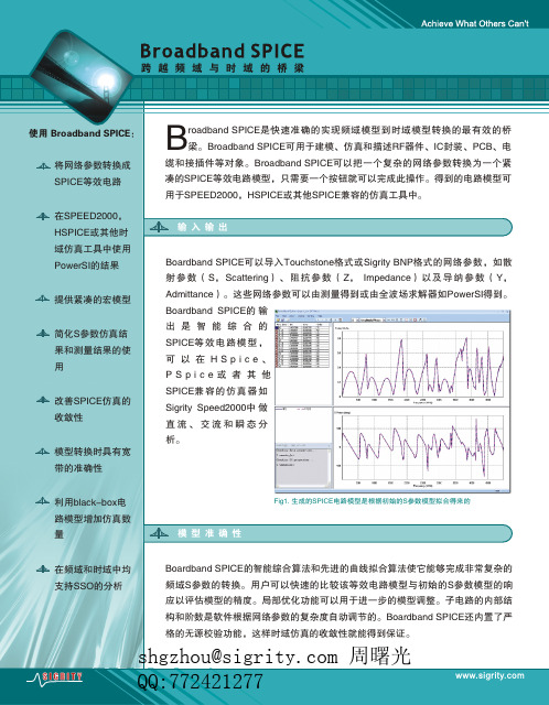
输入输出模型准确性Fig1. 生成的SPICE电路模型是根据初始的S参数模型拟合得来的shgzhou@ 周曙光QQ:772421277首先用PowerSI导入IC封装和PCB的设计文件,这些文件可以来自Sigrity、Cadence、Mentor Graphics、Altium和Zuken等任何一款布线产品。
Broadband-spice speedxp sigrity
Boardband SPICE可以导入Touchstone格式或Sigrity BNP格式的网络参数,如散射参数(S,Scattering)、阻抗参数(Z, Impedance)以及导纳参数(Y,Admittance)。
这些网络参数可以由测量得到或由全波场求解器如PowerSI得到。
Boardband SPICE的输出是智能综合的SPICE等效电路模型,可以在H S p i c e 、P S p i c e 或者其他SPICE兼容的仿真器如Sigrity Speed2000中做直流、交流和瞬态分析。
使用 Broadband SPICE:将网络参数转换成SPICE等效电路在SPEED2000,HSPICE或其他时域仿真工具中使用PowerSI的结果提供紧凑的宏模型简化S参数仿真结果和测量结果的使用改善SPICE仿真的收敛性模型转换时具有宽带的准确性利用black-box电路模型增加仿真数量在频域和时域中均支持SSO的分析roadband SPICE是快速准确的实现频域模型到时域模型转换的最有效的桥B 梁。
Broadband SPICE可用于建模、仿真和描述RF器件、IC封装、PCB、电缆和接插件等对象。
Broadband SPICE可以把一个复杂的网络参数转换为一个紧凑的SPICE等效电路模型,只需要一个按钮就可以完成此操作。
得到的电路模型可用于SPEED2000,HSPICE或其他SPICE兼容的仿真工具中。
Boardband SPICE的智能综合算法和先进的曲线拟合算法使它能够完成非常复杂的频域S参数的转换。
用户可以快速的比较该等效电路模型与初始的S参数模型的响应以评估模型的精度。
局部优化功能可以用于进一步的模型调整。
子电路的内部结构和阶数是软件根据网络参数的复杂度自动调节的。
Boardband SPICE还内置了严格的无源校验功能,这样时域仿真的收敛性就能得到保证。
输入输出模型准确性Fig1. 生成的SPICE电路模型是根据初始的S参数模型拟合得来的shgzhou@ 周曙光QQ:772421277首先用PowerSI导入IC封装和PCB的设计文件,这些文件可以来自Sigrity、Cadence、Mentor Graphics、Altium和Zuken等任何一款布线产品。
Si1153 光线传感器与接近传感器 IC说明书

Si1153 Data ShortProximity/Ambient Light Sensor IC with I 2C InterfaceThe Si1153-AA00/AA09/AA9x is an ambient light sensor, proximity, and gesture detec-tor with I 2C digital interface and programmable-event interrupt output.This touchless sensor IC includes dual 23-bit analog-to-digital converters, an integrated high-sensitivity array of visible and infrared photodiodes, a digital signal processor, and three integrated LED drivers with programmable drive levels. The Si1153 offers excel-lent performance under a wide dynamic range and a variety of light sources, including direct sunlight. The Si1153 can also work under dark glass covers. The photodiode re-sponse and associated digital conversion circuitry provide excellent immunity to artificial light flicker noise and natural light flutter noise. With two or more LEDs, the Si1153 is capable of supporting multiple-axis proximity motion detection. The Si1153 is provided in a 10-lead 2x2 mm DFN package or in a 10-lead 2.9x4.9 mm LGA module with integra-ted LED, and is capable of operation from 1.62 to 3.6 V over the –40 to +85 °C tempera-ture range.Applications:•Wearables •Handsets•Display backlighting control •Consumer electronicsLED1LED2 *LED3 **LIGHT** Pull up to VDD with 47 kOhm resistor* Pull up to VDD with 47 kOhm resistor to select primary I2C address (0x53), or down to GND for alt I2C address 0x52. Rev. 0.9Si1153 LGA Module Basic ApplicationPin Description 2.85x4.9 mm LGA ModuleSi1153 DFN Basic Application Pin Description 2x2 mm DFNTable 1.1. Recommended Operating ConditionsTable 1.2. Ordering GuideSi1153 Data Short | Smart. Connected. Energy-friendly.Rev. 0.9 | 1DisclaimerSilicon Laboratories intends to provide customers with the latest, accurate, and in-depth documentation of all peripherals and modules available for system and software implementers using or intending to use the Silicon Laboratories products. Characterization data, available modules and peripherals, memory sizes and memory addresses refer to each specific device, and "Typical" parameters provided can and do vary in different applications. Application examples described herein are for illustrative purposes only. Silicon Laboratories reserves the right to make changes without further notice and limitation to product information, specifications, and descriptions herein, and does not give warranties as to the accuracy or completeness of the included information. Silicon Laboratories shall have no liability for the consequences of use of the information supplied herein. This document does not imply or express copyright licenses granted hereunder to design or fabricate any integrated circuits. The products must not be used within any Life Support System without the specific written consent of Silicon Laboratories. A "Life Support System" is any product or system intended to support or sustain life and/or health, which, if it fails, can be reasonably expected to result in significant personal injury or death. Silicon Laboratories products are generally not intended for military applications. Silicon Laboratories products shall under no circumstances be used in weapons of mass destruction including (but not limited to) nuclear, biological or chemical weapons, or missiles capable of delivering such weapons.Trademark InformationSilicon Laboratories Inc., Silicon Laboratories, Silicon Labs, SiLabs and the Silicon Labs logo, CMEMS®, EFM, EFM32, EFR, Energy Micro, Energy Micro logo and combinations thereof, "the world’s most energy friendly microcontrollers", Ember®, EZLink®, EZMac®, EZRadio®, EZRadioPRO®, DSPLL®, ISOmodem ®, Precision32®, ProSLIC®, SiPHY®, USBXpress® and others are trademarks or registered trademarks of Silicon Laboratories Inc. ARM, CORTEX, Cortex-M3 and THUMB are trademarks or registered trademarks of ARM Holdings. Keil is a registered trademark of ARM Limited. All other products or brand names mentioned herein are trademarks of their respective holders.Silicon Laboratories Inc.400 West Cesar Chavez Austin, TX 78701USASmart.Connected.Energy-FriendlyProducts/productsQuality/qualitySupport and Community。
小信号放大电路图详解

小信号放大电路图详解小 信号放大一直是电子设计竞赛经久不衰的题目,也是工程师们设计电路时经常遇到的问题。
作者历经小信号放大的血泪史,介绍了小信号放大中的集成芯片放大电 路、滤波器电路和分立元件放大器,有详细的电路图讲解哦!其中LC无源滤波器的软件设计、仿真以及硬件制作流程也合适很多其他电路设计。
第一部分:集成芯片放大器电路图讲解不知有多少童鞋知道TI公司的LHM6624。
这个芯片对于作者来说那是福星一枚。
其主要技术指标如下:Single/Dual Ultra Low Noise Wideband Operational Amplifier(单/双电源低噪声宽带小信号放大器);其增益带宽积在单电源供电时可达1.5GHz,双电源供电时可达1.3GHz;供电电压双电源 (± 2.5V to ± 6V)单电源(+5V to +12V);摆率(Slew rate) 350V/μs增益为10dB(AV = 10)时摆率400V/μs;输入噪声0.92nV/;输入失调电压典型值700uV 。
应用电路图如下:其中双电源供电±5V,C12,C13作用是电源滤波,即稳压;输入阻抗为50W;输出信号峰峰值可至8V(最好不要超过3V,因为大信号会出现非线性放 大)。
这是一个典型的同相放大器,放大倍数计算公式为AV=R14/R12,图中参数放大倍数20倍,即26dB。
值得注意的一点是电阻R16的作用:调 节零漂~如果对低频放大没什么特别需要的话,此处电阻R13,R16以及C11都可省略,但是如果想要放大直流信号的话,此处调节电路就十分有必要了。
模拟放大电路的电源滤波处理是十分有必要的,目的是防止高频模拟信号影响污染整个电源系统。
图中C12,C13在pcb中的位置要尽量靠近IC的电源入 口。
另外也可选择把磁珠(要求严格时可用电感,要求不高时可用100W电阻)和两个电容组成p形滤波电路, 这样可以把电源中的噪音滤得干干净净~2:滤波器滤波器分为有源滤波器和无源滤波器两种,区别在于有没有外接电源。
恒星芯片B4161A 2.4GHz 19dBm无线芯片板文档说明书

EFR32MG12 2.4 GHz 19 dBm Radio Board BRD4161A Reference ManualRADIO BOARD FEATURES•Wireless SoC:EFR32MG12P432F1024GL125•CPU core: ARM Cortex ®-M4 with FPU •Flash memory: 1024 kB •RAM: 256 kB•Operation frequency: 2.4 GHz •Transmit power: 19 dBm•Integrated PCB antenna, UFL connector (optional).•Touch Slider•Crystals for LFXO and HFXO: 32.768 kHz and 38.4 MHz.The BRD4161A Mighty Gecko Radio Board enables developers to develop Zigbee ®, Thread,Bluetooth ® low energy and proprietary wireless applications. The board con-tains a Mighty Gecko Wireless System on Chip 2.4 GHz and optimized for operation with 19 dBm output power. With the on-board printed antenna and RF connector radi-ated and conducted testing is supported.The BRD4161A Mighty Gecko Radio Board plugs into the Wireless Starter Kit Main-board provided with the Mighty Gecko Starter Kit to get access to display, buttons and additional features from Expansion Boards. With the supporting Simplicity Studio suite of tools, developers can take advantage of graphical wireless application development; mesh networking debug and packet trace; and visual energy profiling and optimization. The board also serves as an RF reference design for applications targeting 2.4 GHz wireless operation with 19 dBm output power.This document contains brief introduction and description of the BRD4161A Radio Board features focusing on the RF sections and performance.| Smart. Connected. Energy-friendly.Rev. 1.00Introduction 1. IntroductionThe EFR32 Mighty Gecko Radio Boards provide a development platform (together with the Wireless Starter Kit Mainboard) for the Silicon Labs EFR32 Mighty Gecko Wireless System on Chips and serve as reference designs for the matching network of the RF inter-face.The BRD4161A Radio Board is designed to operate in the 2400-2483.5 MHz band with the RF matching network optimized to operate with 19 dBm output power.To develop and/or evaluate the EFR32 Mighty Gecko, the BRD4161A Radio Board can be connected to the Wireless Starter Kit Main-board to get access to display, buttons and additional features from Expansion Boards and also to evaluate the performance of the RF interface.2. Radio Board Connector2.1 IntroductionThe board-to-board connector scheme allows access to all EFR32MG12 GPIO pins as well as the RESETn signal. For more informa-tion on the functions of the available pin functions, see the EFR32MG12 data sheet.2.2 Radio Board Connector Pin AssociationsThe figure below shows the pin mapping on the connector to the radio pins and their function on the Wireless Starter Kit Mainboard.GNDF9 / PA3 / VCOM_RTS 3v3VCOM_RTS / PA3 / P36P200Upper RowNC / P38NC / P40PF9 / P42PF11 / P44DEBUG.TMS_SWDIO / PF1 / F0DISP_ENABLE / PD15 / F14UIF_BUTTON0 / PF6 / F12UIF_LED1 / PF4 / F10VCOM_CTS / PA2 / F8DEBUG.RESET / RADIO_#RESET / F4DEBUG.TDO_SWO / PF2 / F2DISP_SI / PC6 / F16VCOM_TXD / PA0 / F6PTI_DATA / PB12 / F20DISP_EXTCOMIN / PD13 / F18USB_VBUS5VBoard ID SCLGNDBoard ID SDAUSB_VREG F7 / PA1 / VCOM_RXD F5 / PA5 / VCOM_ENABLE F3 / PF3 / DEBUG.TDIF1 / PF0 / DEBUG.TCK_SWCLK P45 / PF12P43 / PF10P41 / PF8P39 / NC P37/ PB10 / SENSOR_ENABLE F11 / PF5 / UIF_LED1F13 / PF7 / UIF_BUTTON1F15 / PC8 / DISP_SCLK F17 / PD14 / DISP_SCS F19 / PB13 / PTI_FRAME F21 / PB11 / PTI_CLK GND VMCU_IN PD8 / P0P201Lower RowPD9 / P2PD10 / P4PD11 / P6GNDNCP35 / PA2 / VCOM_CTS P7 / PA9P5 / PA8P3 / PA7P1 / PA6P33 / PA0 / VCOM_TXD P31 / PK2P29 / PK0P27 / PJ14P25 / PI2P23 / PI0P21 / PF14P19 / NC P17 / PC5P15 / PB9P13 / PC11P11 / PB7P9 / PB6VCOM_RXD / P34 / P34BODEN / P32PK1/ P30PJ15 / P28PI3 / P26PI1 / P24PF15 / P22PF13 / P20NC / P18PC4 / P16PB8 / P14PC10 / P12PC9 / P10PD12 / P8Figure 2.1. BRD4161A Radio Board Connector Pin MappingRadio Board Connector3. Radio Board Block Summary3.1 IntroductionThis section gives a short introduction to the blocks of the BRD4161A Radio Board.3.2 Radio Board Block DiagramThe block diagram of the EFR32MG Radio Board is shown in the figure below.Figure 3.1. BRD4161A Block Diagram3.3 Radio Board Block Description3.3.1 Wireless MCUThe BRD4161A Mighty Gecko Radio Board incorporates an EFR32MG12P432F1024GL125 Wireless System on Chip featuring 32-bit Cortex®-M4 with FPU core, 1024 kB of flash memory and 256 kB of RAM and a 2.4 GHz band transceiver with output power up to 19 dBm. For additional information on the EFR32MG12P432F1024GL125, refer to the EFR32MG12 Data Sheet.3.3.2 LF Crystal Oscillator (LFXO)The BRD4161A Radio Board has a 32.768 kHz crystal mounted.3.3.3 HF Crystal Oscillator (HFXO)The BRD4161A Radio Board has a 38.4 MHz crystal mounted.| Smart. Connected. Energy-friendly.Rev. 1.00 | 33.3.4 Matching Network for 2.4 GHzThe BRD4161A Radio Board incorporates a 2.4 GHz matching network which connects the 2.4 GHz TRX pin of the EFR32MG12 to the one on-board printed Inverted-F antenna. The component values were optimized for the 2.4 GHz band RF performace and current con-sumption with 19 dBm output power.For detailed description of the matching network, see Chapter 4.2.1 Description of the 2.4 GHz RF Matching.3.3.5 Inverted-F AntennaThe BRD4161A Radio Board includes a printed Inverted-F antenna (IFA) tuned to have close to 50 Ohm impedance at the 2.4 GHz band.For detailed description of the antenna see Chapter 4.5 Inverted-F Antenna.3.3.6 UFL ConnectorTo be able to perform conducted measurements, Silicon Labs added an UFL connector to the Radio Board. The connector allows an external 50 Ohm cable or antenna to be connected during design verification or testing.Note: By default the output of the matching network is connected to the printed Inverted-F antenna by a series component. It can be connected to the UFL connector as well through a series 0 Ohm resistor which is not mounted by default. For conducted measurements through the UFL connector the series component to the antenna should be removed and the 0 Ohm resistor should be mounted (see Chapter 4.2 Schematic of the RF Matching Network for further details).3.3.7 Radio Board ConnectorsTwo dual-row, 0.05” pitch polarized connectors make up the EFR32MG Radio Board interface to the Wireless Starter Kit Mainboard. For more information on the pin mapping between the EFR32MG12P432F1024GL125 and the Radio Board Connector, refer to Chapter 2.2 Radio Board Connector Pin Associations.3.3.8 Capacitive Touch SliderThe touch slider (T2) utilizes the capacitive touch capability of the Capacitance Sense Module of the EFR32MG12. The slider interpo-lates 4 separate pads to find the exact position of a finger.The figure below shows the pin mapping of the touch slider to the Wireless SoC.Wireless SoCFigure 3.2. Touch Slider Pin MappingRev. 1.00 | 44. RF Section4.1 IntroductionThis section gives a short introduction to the RF section of the BRD4161A.4.2 Schematic of the RF Matching NetworkThe schematic of the RF section of the BRD4161A Radio Board is shown in the following figure.2.4 GHz Matching 2.4 GHz RF OutputSelection & Inverted-F AntennaFigure 4.1. Schematic of the RF Section of the BRD4161A4.2.1 Description of the 2.4 GHz RF MatchingThe 2.4 GHz matching connects the 2G4RF_IOP pin to the on-board printed Inverted-F Antenna. The 2G4RF_ION pin is connected to ground. For higher output powers (13 dBm and above), besides the impedance matching circuitry, it is recommended to use additional harmonic filtering as well at the RF output. The targeted output power of the BRD4161A board is 19 dBm. Therefore, the RF output of the IC is connected to the antenna through a four-element impedance matching and harmonic filter circuitry.For conducted measurements the output of the matching network can also be connected to the UFL connector by removing the series R1 component between the antenna and the output of the matching and adding a 0 Ohm resistor to the R2 resistor position between the output of the matching and the UFL connector.4.3 RF Section Power SupplyOn the BRD4161A Radio Board the power supply pins of the RF section (RFVDD, PAVDD) are directly connected to the output of the on-chip DC-DC converter. This way, by default, the DC-DC converter provides 1.8 V for the entire RF section (for details, see the sche-matic of the BRD4161A).4.4 Bill of Materials for the 2.4 GHz MatchingThe Bill of Materials of the 2.4 GHz matching network of the BRD4161A Radio Board is shown in the following table.| Smart. Connected. Energy-friendly.Rev. 1.00 | 5Table 4.1. Bill of Materials for the BRD4161A 2.4GHz RF Matching Network4.5 Inverted-F AntennaThe BRD4161A Radio Board includes an on-board printed Inverted-F Antenna tuned for the 2.4 GHz band. Due to the design restric-tions of the Radio Board, the input of the antenna and the output of the matching network can't be placed directly next to each other. As a result, a 50 Ohm transmission line was necessary to connect them. With the actual line length the impedance of the antenna at the double-harmonic frequency is transformed closer to a "critical load impedance range" resulting in the radiated level of the harmonic increases.To reduce the harmonic radiation a tuning component was used between the matching network output and the antenna input. For the actual Radio Board design (with the actual transmission line length) a small value inductor was used (instead of the R1 resistor with value of 1.8 nH) to transform the impedance at the double-frequency harmonic away from the critical region while keeping the impe-dance at the funamental close to 50 Ohm. With this the suppression of the radiated double-frequency harmonic increases by approxi-mately 3-4 dB. The resulting impedance and reflection measured at the output of the matcing network are shown in the following figure. As it can be observed the impedance is close to 50 Ohm (the reflection is better than -10 dB) for the entire 2.4 GHz band.Figure 4.2. Impedance and Reflection of the Inverted-F Antenna of the BRD4161A Board Measured from the Matching Output Note: The same value and type of 1.8 nH inductor was used as the one in the matching network (L1). | Smart. Connected. Energy-friendly.Rev. 1.00 | 65. Mechanical DetailsThe BRD4161A Mighty Gecko Radio Board is illustrated in the figures below.Figure 5.1. BRD4161A Top View24 mmConnectorConnector Figure 5.2. BRD4161A Bottom ViewMechanical DetailsRev. 1.00 | 7EMC Compliance 6. EMC Compliance6.1 IntroductionCompliance of the fundamental and harmonic levels is tested against the following standards:• 2.4 GHz:•ETSI EN 300-328•FCC 15.2476.2 EMC Regulations for 2.4 GHz6.2.1 ETSI EN 300-328 Emission Limits for the 2400-2483.5 MHz BandBased on ETSI EN 300-328 the allowed maximum fundamental power for the 2400-2483.5 MHz band is 20 dBm EIRP. For the unwan-ted emissions in the 1 GHz to 12.75 GHz domain the specified limit is -30 dBm EIRP.6.2.2 FCC15.247 Emission Limits for the 2400-2483.5 MHz BandFCC 15.247 allows conducted output power up to 1 Watt (30 dBm) in the 2400-2483.5 MHz band. For spurious emmissions the limit is -20 dBc based on either conducted or radiated measurement, if the emission is not in a restricted band. The restricted bands are speci-fied in FCC 15.205. In these bands the spurious emission levels must meet the levels set out in FCC 15.209. In the range from 960 MHz to the frequency of the 5th harmonic it is defined as 0.5 mV/m at 3 m distance (equals to -41.2 dBm in EIRP).Additionally, for spurious frequencies above 1 GHz, FCC 15.35 allows duty-cycle relaxation to the regulatory limits. For the EmberZNet PRO the relaxation is 3.6 dB. Therefore, the -41.2 dBm limit can be modified to -37.6 dBm.If operating in the 2400-2483.5 MHz band the 2nd, 3rd and 5th harmonics can fall into restricted bands. As a result, for those the -37.6 dBm limit should be applied. For the 4th harmonic the -20 dBc limit should be applied.6.2.3 Applied Emission Limits for the 2.4 GHz BandThe above ETSI limits are applied both for conducted and radiated measurements.The FCC restricted band limits are radiated limits only. Besides that, Silicon Labs applies those to the conducted spectrum i.e., it is assumed that, in case of a custom board, an antenna is used which has 0 dB gain at the fundamental and the harmonic frequencies. In that theoretical case, based on the conducted measurement, the compliance with the radiated limits can be estimated.The overall applied limits are shown in the table below.Table 6.1. Applied Limits for Spurious Emissions for the 2.4 GHz Band | Smart. Connected. Energy-friendly.Rev. 1.00 | 87. RF Performance7.1 Conducted Power MeasurementsDuring measurements, the EFR32MG Radio Board was attached to a Wireless Starter Kit Mainboard which was supplied by USB. The voltage supply for the Radio Board was 3.3 V.7.1.1 Conducted Measurements in the 2.4 GHz bandThe BRD4161A board was connected directly to a Spectrum Analyzer through its UFL connector (the R1 component was removed and a 0 Ohm resistor was soldered to the R2 resistor position). During measurements, the voltage supply for the board was 3.3 V provided by the mainboard. The supply for the radio (RFVDD) was 1.8 V provided by the on-chip DC-DC converter, the supply for the power amplifier (PAVDD) was 3.3 V (for details, see the schematic of the BRD4161A). The transceiver was operated in continuous carrier transmission mode. The output power of the radio was set to 19 dBm.The typical output spectrum is shown in the following figure.Figure 7.1. Typical Output Spectrum of the BRD4161AAs it can be observed, the fundamental is slightly lower than 19 dBm limit and the strongest unwanted emission is the double-frequency harmonic and it is under the -37.6 dBm applied limit.Note: The conducted measurement is performed by connecting the on-board UFL connector to a Spectrum Analyzer through an SMA Conversion Adapter (P/N: HRMJ-U.FLP(40)). This connection itself introduces approximately 0.3 dB insertion loss.RF PerformanceRev. 1.00 | 97.2 Radiated Power MeasurementsDuring measurements, the EFR32MG Radio Board was attached to a Wireless Starter Kit Mainboard which was supplied by USB. The voltage supply for the Radio Board was 3.3 V. The radiated power was measured in an antenna chamber by rotating the DUT 360degrees with horizontal and vertical reference antenna polarizations in the XY , XZ and YZ cuts. The measurement axes are shown inthe figure below.Figure 7.2. DUT: Radio Board with the Wireless Starter Kit Mainboard (Illustration)Note: The radiated measurement results presented in this document were recorded in an unlicensed antenna chamber. Also the radi-ated power levels may change depending on the actual application (PCB size, used antenna, and so on). Therefore, the absolute levels and margins of the final application are recommended to be verified in a licensed EMC testhouse.7.2.1 Radiated Measurements in the 2.4 GHz bandFor the transmitter antenna the on-board printed Inverted-F antenna of the BRD4161A board was used (the R1 component was moun-ted). During measurements, the board was attached to a Wireless Starter Kit Mainboard (BRD4001 (Rev. A02) ) which was supplied through USB. During the measurements the voltage supply for the board was 3.3 V provided by the mainboard. The supply for the radio (RFVDD) was 1.8 V provided by the on-chip DC-DC converter, the supply for the power amplifier (PAVDD) was 3.3 V (for details, see the schematic of the BRD4161A). The transceiver was operated in continuous carrier transmission mode. The output power of the radio was set to 19 dBm based on the conducted measurement.The results are shown in the table below.Table 7.1. Maximums of the measured radiated powers in EIRP [dBm]As it can be observed, thanks to the high gain of the Inverted-F antenna, the level of the fundamental is higher than 19 dBm. The stron-gest harmonic is the double-frequency one and thanks to the additional suppression provided by the instead of the R1 resistor its level is under -50 dBm.RF PerformanceEMC Compliance Recommendations 8. EMC Compliance Recommendations8.1 Recommendations for 2.4 GHz ETSI EN 300-328 complianceAs it was shown in the previous chapter, the radiated power of the fundamental of the BRD4161A Mighty Gecko Radio Board complies with the 20 dBm limit of the ETSI EN 300-328 in case of the conducted measurement but due to the high antenna gain the radiated power is higher than the limit by 2 dB. In order to comply, the output power should be reduced (with different antennas, depending on the gain of the used antenna, the necessary reduction can be different). The harmonic emissions are under the -30 dBm limit. Although the BRD4161A Radio Board has an option for mounting a shielding can, that is not required for the compliance.8.2 Recommendations for 2.4 GHz FCC 15.247 complianceAs it was shown in the previous chapter, the radiated power of the fundamental of the BRD4161A Mighty Gecko Radio Board complies with the 30 dBm limit of the FCC 15.247. The harmonic emissions are under the -37.6 dBm applied limit both in case of the conducted and the radiated measurements. Although the BRD4161A Radio Board has an option for mounting a shielding can, that is not required for the compliance.Document Revision History 9. Document Revision HistoryTable 9.1. Document Revision HistoryBoard Revision History 10. Board Revision HistoryTable 10.1. BRD4161A Radio Board RevisionsErrata 11. ErrataThere are no known errata at present.Table of Contents1. Introduction (1)2. Radio Board Connector (2)2.1 Introduction (2)2.2 Radio Board Connector Pin Associations (2)3. Radio Board Block Summary (3)3.1 Introduction (3)3.2 Radio Board Block Diagram (3)3.3 Radio Board Block Description (3)3.3.1 Wireless MCU (3)3.3.2 LF Crystal Oscillator (LFXO) (3)3.3.3 HF Crystal Oscillator (HFXO) (3)3.3.4 Matching Network for 2.4 GHz (4)3.3.5 Inverted-F Antenna (4)3.3.6 UFL Connector (4)3.3.7 Radio Board Connectors (4)3.3.8 Capacitive Touch Slider (4)4. RF Section (5)4.1 Introduction (5)4.2 Schematic of the RF Matching Network (5)4.2.1 Description of the 2.4 GHz RF Matching (5)4.3 RF Section Power Supply (5)4.4 Bill of Materials for the 2.4 GHz Matching (5)4.5 Inverted-F Antenna (6)5. Mechanical Details (7)6. EMC Compliance (8)6.1 Introduction (8)6.2 EMC Regulations for 2.4 GHz (8)6.2.1 ETSI EN 300-328 Emission Limits for the 2400-2483.5 MHz Band (8)6.2.2 FCC15.247 Emission Limits for the 2400-2483.5 MHz Band (8)6.2.3 Applied Emission Limits for the 2.4 GHz Band (8)7. RF Performance (9)7.1 Conducted Power Measurements (9)7.1.1 Conducted Measurements in the 2.4 GHz band (9)7.2 Radiated Power Measurements (10)7.2.1 Radiated Measurements in the 2.4 GHz band (10)8. EMC Compliance Recommendations (11)8.1 Recommendations for 2.4 GHz ETSI EN 300-328 compliance (11)8.2 Recommendations for 2.4 GHz FCC 15.247 compliance (11)9. Document Revision History (12)10. Board Revision History (13)11. Errata (14)Table of Contents (15)Silicon Laboratories Inc.400 West Cesar Chavez Austin, TX 78701USASimplicity StudioOne-click access to MCU and wireless tools, documentation, software, source code libraries & more. Available for Windows, Mac and Linux!IoT Portfolio /IoTSW/HW/simplicityQuality/qualitySupport and CommunityDisclaimerSilicon Labs intends to provide customers with the latest, accurate, and in-depth documentation of all peripherals and modules available for system and software implementers using or intending to use the Silicon Labs products. Characterization data, available modules and peripherals, memory sizes and memory addresses refer to each specific device, and "Typical" parameters provided can and do vary in different applications. Application examples described herein are for illustrative purposes only. Silicon Labs reserves the right to make changes without further notice and limitation to product information, specifications, and descriptions herein, and does not give warranties as to the accuracy or completeness of the included information. Silicon Labs shall have no liability for the consequences of use of the information supplied herein. This document does not imply or express copyright licenses granted hereunder to design or fabricate any integrated circuits. The products are not designed or authorized to be used within any Life Support System without the specific written consent of Silicon Labs. A "Life Support System" is any product or system intended to support or sustain life and/or health, which, if it fails, can be reasonably expected to result in significant personal injury or death. Silicon Labs products are not designed or authorized for military applications. Silicon Labs products shall under no circumstances be used in weapons of mass destruction including (but not limited to) nuclear, biological or chemical weapons, or missiles capable of delivering such weapons.Trademark InformationSilicon Laboratories Inc.® , Silicon Laboratories®, Silicon Labs®, SiLabs® and the Silicon Labs logo®, Bluegiga®, Bluegiga Logo®, Clockbuilder®, CMEMS®, DSPLL®, EFM®, EFM32®, EFR, Ember®, Energy Micro, Energy Micro logo and combinations thereof, "the world’s most energy friendly microcontrollers", Ember®, EZLink®, EZRadio®, EZRadioPRO®, Gecko®, ISOmodem®, Precision32®, ProSLIC®, Simplicity Studio®, SiPHY®, Telegesis, the Telegesis Logo®, USBXpress® and others are trademarks or registered trademarks of Silicon Labs. ARM, CORTEX, Cortex-M3 and THUMB are trademarks or registered trademarks of ARM Holdings. Keil is a registered trademark of ARM Limited. All other products or brand names mentioned herein are trademarks of their respective holders.。
PowerDC分析基础_100621

用what-if分析来改善设计
Original VRM pins After turn the VRM 180 degree around (Done inside PowerDC GUI)
34
5. Package中的直流分析
35
GND平面上的IR Drop分布
Hotspots
36
发现大的过孔电流
R=V/I。
σ为材料的电导率,铜的电导率为 5.8 x 10⁷ S/m
12
电流密度
自由电荷在导体中流动形成传导电流,其密度为 导电媒质中的恒流电场的基本方程为
电源/地平面上的电流密度是矢量分布,而平面上的标 量电流是没有物理意义的
13
PowerDC的主要功能
9
PowerDC的算法及理论基础
PowerDC基于电磁场理论求出电源/地平面上的电压
分布、电流密度的矢量分布,过孔电流和电阻。
全新的FEM仿真引擎在仿真精度和效率上有了很大的
提升。其精细的三角形网格剖分比其他工具采用的矩 形网格在计算结果和显示精度上要先进很多,另外特 有的快速算法使工具即使在仿真大型PCB时也仅需数 分钟的时间。
27
电源走线宽度计算器
28
4. PCB中的直流分析
29
电源平面
30
结果
9
31
过孔电流
Hotspot identifier
大量电流通过黄色过孔,贯穿2个 电源平面的重叠部分。
32
发现第11层上的高电流密度
高电流密度
显示电流密度在 5mA/mil^2 及以上的部分;小于该指标的以灰色来显示。
Canddence Sigrity中用Power SI进行DDR3走线阻抗与耦合检查分析

Canddence Sigrity中用Power SI进行走线阻抗与耦合检查分析(组件ERC->Trace Imp/cpl/ref check)基于信号完整性考虑,检查PCB阻抗和其耦合串扰是否满足要求,是硬件工程师的必要工作。
对于有较多高速或信号线的PCB来说,手动检查费时费力效果也不好,非常容易漏掉一些关键点,有必要寻找一种自动检查的方法。
如下介绍基于仿真软件Sigrity的自动检查,其快速、准确,不仅降低了工程师的工作量,且改善了检查的结果,有利于PCB的优化。
Sigrity软件Power SI进行走线阻抗与耦合检查分析有两点需要注意:第一个是这个功能计算出来的阻抗和SI9000会有一点偏差。
第二个是其耦合度检查只能检查同层之间的耦合,对于不同层之间的耦合还无法进行检查。
不过在绝大多数的设计中,现有的这个功能已经够用了,通过这个方式可以非常快速的对整版或是重点关注的信号进行阻抗及耦合的检查,找到设计的薄弱环节进行整改。
3.2.1 阻抗和耦合阻抗:在具有电阻、电感和电容的电路里,对交流电所起的阻碍作用叫做阻抗。
阻抗常用Z 表示;的复杂性、调用模块的方式以及通过界面传送数据的多少?2片32位DDR3阻抗和耦合分析为例3.3 以仿XC7Z010CLG400与修改成实际的板厚、基材等信息。
要根据厂家的信息来填写。
材料参数:可以通过view Material按钮查看。
焊盘的设置:环氧树脂是BT;Er为材料的介电常数;Loss tangent损耗因数;Detect and model the coplanar traces共面轨迹的检测与建模>Setup 选取器件:器件选择把要仿真的网络对应的器件(这里面我们选端要赋予正极的标注。
选择发送端芯片或内存控制器或者直接找,输入U1;网络我们之前已经选择过,该步骤直接跳过,点击下一步。
串阻之间的value值需要补上,根据实际情况,比如22欧姆或33欧姆。
半导体组件工业公司

CS8221Micropower 5.0 V, 100 mA Low Dropout Linear RegulatorThe CS8221 is a precision 5.0 V, 100 mA micropower voltage regulator with very low quiescent current (60 m A typical at 100 m A load). The 5.0 V output is accurate within ±2.0% and supplies 100 mA of load current with a maximum dropout voltage of only 600 mV. The regulator is protected against reverse battery, short circuit, overvoltage, and over temperature conditions. The device can withstand 74 V peak transients making it suitable for use in automotive environments. The CS8221 is pin for pin compatible with the LM2931. Features•Low Quiescent Current (60 m A @ 100 m A Load)•5.0 V ±2.0% Output•100 mA Output Current Capability •Internally Fused Leads in SO−8 Package •Fault Protection−+74 V Peak Transient V oltage−−15 V Reverse V oltage−Short Circuit−Thermal Shutdown•These are Pb−Free DevicesPIN CONNECTIONS ANDMARKING INDIAGRAMDevice Package Shipping†ORDERING INFORMATION*D2PAK−3(Pb−Free)CS8221YDP3G50 Units/RailCS8221= Specific Device CodeA= Assembly LocationWL, L= Wafer LotY= YearWW, W= Work WeekG or G= Pb−Free PackageSO−8DF SUFFIXCASE 751INVCS8221AWLYWWG1Tab = GNDPin 1. V IN2. GND3. V OUTD2PAK−3CS8221YDPR3G D2PAK−3(Pb−Free)750/T ape & Reel*Contact your local sales representative for TO−92 package option.†For information on tape and reel specifications, including part orientation and tape sizes, please refer to our Tape and Reel Packaging Specification Brochure, BRD8011/D.D2PAK−3DP SUFFIXCASE 418ABCS8221YDFR8G2500/T ape & ReelSO−8(Pb−Free)Figure 1. Block DiagramGNDV OUTV INABSOLUTE MAXIMUM RATINGS*RatingValue Unit Junction Temperature Range, T J−40 to +150°C Storage Temperature Range, T STORAGE −55 to +150°C Power DissipationInternally Limited−Peak Transient Voltage (60 V Load Dump @ V IN = 14 V)−15, 74V Input Operating Range −0.5 to 26V Output CurrentInternally Limited−Electrostatic Discharge (Human Body Model) 2.0kV Lead Temperature Soldering:Reflow (Note 1)230 peak°CStresses exceeding Maximum Ratings may damage the device. Maximum Ratings are stress ratings only. Functional operation above the Recommended Operating Conditions is not implied. Extended exposure to stresses above the Recommended Operating Conditions may affect device reliability.1.60 seconds maximum above 183°.*The maximum package power dissipation must be observed.ELECTRICAL CHARACTERISTICS (6.0 ≤ V IN ≤26 V , I OUT = 1.0 mA, −40°C ≤ T J ≤125°C unless otherwise noted.)CharacteristicTest ConditionsMinTypMaxUnitOutput Stage Output Voltage, V OUT9.0 V < V IN < 26 V, 100 m A ≤I OUT ≤ 100 mA 6.0 V ≤ V IN ≤ 26 V, 100 m A ≤I OUT ≤ 100 mA 4.94.85 5.05.0 5.15.15V V Dropout Voltage (V IN − V OUT )I OUT = 100 mA I OUT = 100 m A−−400100600150mV mV Load Regulation V IN = 14 V , 100 m A ≤I OUT ≤100 mA,− 5.050mV Line Regulation 6.0 V < V < 26 V, I OUT = 1.0 mA − 5.050mV Quiescent Current, (I Q )I OUT = 100 m A, V IN = 6.0 V I OUT = 50 mA I OUT = 100 mA−−−604.0121206.020m A mA mA Ripple Rejection 7.0 ≤ V IN ≤ 17 V , I OUT = 100 mA, f = 120 Hz6075−dB Current Limit−125200−mAShort Circuit Output Current V OUT = 0 V40125−m A Thermal Shutdown (Note 2)−150180−°C Overvoltage ShutdownV OUT ≤ 1.0 V303438V2.This parameter is guaranteed by design, but not parametrically tested in production.PACKAGE LEAD DESCRIPTIONPACKAGE LEAD #LEAD SYMBOLFUNCTIONSO −8D 2PAK −313V OUT 5.0 V, ±2.0%, 100 mA Output.2, 3, 6, 72GND Ground.4−NC No Connection.5−NC No Connection.81V INInput Voltage.TYPICAL PERFORMANCE CHARACTERISTICSFigure 2. CS8221 Output StabilityE S R (W )I OUT OUTPUT CURRENTCIRCUIT DESCRIPTIONVOLTAGE REFERENCE AND OUTPUT CIRCUITRY Output Stage ProtectionThe output stage is protected against overvoltage, short circuit and thermal runaway conditions (Figure 3).Figure 3. Typical Circuit Waveforms for OutputStage ProtectionILoad DumpV VThermal ShutdownShort CircuitIf the input voltage rises above 30 V , the output shuts down. This response protects the internal circuitry and enables the IC to survive unexpected voltage transients.Should the junction temperature of the power device exceed 180°C (typ) the power transistor is turned off.Thermal shutdown is an effective means to prevent die overheating since the power transistor is the principle heat source in the IC.Figure 4. Application and Test Diagram*C 1 is required if regulator is far from the power source filter .**C 2 is required for stability.APPLICATION NOTESSTABILITY CONSIDERATIONSThe output or compensation capacitor helps determine three main characteristics of a linear regulator: start −up delay, load transient response and loop stability.The capacitor value and type should be based on cost,availability, size and temperature constraints. A tantalum or aluminum electrolytic capacitor is best, since a film or ceramic capacitor with almost zero ESR can cause instability. The aluminum electrolytic capacitor is the least expensive solution, but, if the circuit operates at low temperatures (−25°C to −40°C), both the value and ESR of the capacitor will vary considerably. The capacitor manufacturers data sheet usually provides this information.The value for the output capacitor C OUT shown in Figure 4 should work for most applications, however it is not necessarily the optimized solution.To determine an acceptable value for C OUT for a particular application, start with a tantalum capacitor of the recommended value and work towards a less expensive alternative part.Step 1: Place the completed circuit with a tantalum capacitor of the recommended value in an environmental chamber at the lowest specified operating temperature and monitor the outputs with an oscilloscope. A decade box connected in series with the capacitor will simulate the higher ESR of an aluminum capacitor. Leave the decade box outside the chamber, the small resistance added by the longer leads is negligible.Step 2: With the input voltage at its maximum value,increase the load current slowly from zero to full load while observing the output for any oscillations. If no oscillations are observed, the capacitor is large enough to ensure a stable design under steady state conditions.Step 3: Increase the ESR of the capacitor from zero using the decade box and vary the load current until oscillations appear. Record the values of load current and ESR that cause the greatest oscillation. This represents the worst case load conditions for the regulator at low temperature.Step 4: Maintain the worst case load conditions set in step 3 and vary the input voltage until the oscillations increase. This point represents the worst case input voltage conditions.Step 5: If the capacitor is adequate, repeat steps 3 and 4with the next smaller valued capacitor. A smaller capacitor will usually cost less and occupy less board space. If the output oscillates within the range of expected operating conditions, repeat steps 3 and 4 with the next larger standard capacitor value.Step 6: Test the load transient response by switching in various loads at several frequencies to simulate its real working environment. Vary the ESR to reduce ringing.Step 7: Increase the temperature to your highest operating temperature. V ary the load current as instructed in step 5 to test for any oscillations.Once the minimum capacitor value with the maximum ESR is found, a safety factor should be added to allow for the tolerance of the capacitor and any variations in regulator performance. Most good quality aluminum electrolytic capacitors have a tolerance of ± 20% so the minimum value found should be increased by at least 50% to allow for this tolerance plus the variation which will occur at low temperatures. The ESR of the capacitor should be less than 50% of the maximum allowable ESR found in step 3 above.CALCULATING POWER DISSIPATION IN A SINGLEOUTPUT LINEAR REGULATORThe maximum power dissipation for a single output regulator (Figure 5) is:P D(max)+NJV IN(max)*V OUT(min)NjI OUT(max))V IN(max)I Q(1)where:V IN(max) is the maximum input voltage,V OUT(min) is the minimum output voltage,I OUT(max) is the maximum output current for the application, andI Q is the quiescent current the regulator consumes at I OUT(max).Once the value of P D(max) is known, the maximum permissible value of R ΘJA can be calculated:R Q JA +(2)The value of R ΘJA can then be compared with those in the package section of the data sheet. Those packages with R ΘJA ’s less than the calculated value in equation 2 will keep the die temperature below 150°C.In some cases, none of the packages will be sufficient to dissipate the heat generated by the IC, and an external heatsink will be required.Figure 5. Single Output Regulator With KeyPerformance Parameters LabeledV INV OUTHEAT SINKSA heat sink effectively increases the surface area of the package to improve the flow of heat away from the IC and into the surrounding air.Each material in the heat flow path between the IC and the outside environment will have a thermal resistance. Like series electrical resistances, these resistances are summed to determine the value of R ΘJA .R Q JA +R Q JC )R Q CS )R Q SA(3)where:R ΘJC = the junction −to −case thermal resistance,R ΘCS = the case −to −heatsink thermal resistance, and R ΘSA = the heatsink −to −ambient thermal resistance.R ΘJC appears in the package section of the data sheet. Like R ΘJA , it too is a function of package type. R ΘCS and R ΘSA are functions of the package type, heatsink and the interface between them. These values appear in heat sink data sheets of heat sink manufacturers.SMART REGULATOR is a registered trademark of Semiconductor Components Industries, LLC (SCILLC).MECHANICAL CASE OUTLINE PACKAGE DIMENSIONSON Semiconductor and are registered trademarks of Semiconductor Components Industries, LLC (SCILLC). SCILLC reserves the right to make changes without further notice to any products herein. SCILLC makes no warranty, representation or guarantee regarding the suitability of its products for any particular purpose, nor does SCILLC assume any liability arising out of the application or use of any product or circuit, and specifically disclaims any and all liability, including without limitation special, consequential or incidental damages.“Typical” parameters which may be provided in SCILLC data sheets and/or specifications can and do vary in different applications and actual performance may vary over time. All operating parameters, including “Typicals” must be validated for each customer application by customer’s technical experts. SCILLC does not convey any license under its patent rights nor the rights of others. SCILLC products are not designed, intended, or authorized for use as components in systems intended for surgical implant into the body, or other applications intended to support or sustain life, or for any other application in which the failure of the SCILLC product could create a situation where personal injury or death may occur. Should Buyer purchase or use SCILLC products for any such unintended or unauthorized application, Buyer shall indemnify and hold SCILLC and its officers, employees, subsidiaries, affiliates,and distributors harmless against all claims, costs, damages, and expenses, and reasonable attorney fees arising out of, directly or indirectly, any claim of personal injury or deathSOIC −8 NB CASE 751−07ISSUE AKDATE 16 FEB 2011NOTES:1.DIMENSIONING AND TOLERANCING PER ANSI Y14.5M, 1982.2.CONTROLLING DIMENSION: MILLIMETER.3.DIMENSION A AND B DO NOT INCLUDE MOLD PROTRUSION.4.MAXIMUM MOLD PROTRUSION 0.15 (0.006)PER SIDE.5.DIMENSION D DOES NOT INCLUDE DAMBAR PROTRUSION. ALLOWABLE DAMBARPROTRUSION SHALL BE 0.127 (0.005) TOTAL IN EXCESS OF THE D DIMENSION AT MAXIMUM MATERIAL CONDITION.6.751−01 THRU 751−06 ARE OBSOLETE. NEW STANDARD IS 751−07.SCALE 1:1STYLES ON PAGE 2DIM A MIN MAX MIN MAX INCHES4.805.000.1890.197MILLIMETERSB 3.80 4.000.1500.157C 1.35 1.750.0530.069D 0.330.510.0130.020G 1.27 BSC 0.050 BSC H 0.100.250.0040.010J 0.190.250.0070.010K 0.40 1.270.0160.050M 0 8 0 8 N 0.250.500.0100.020S5.806.200.2280.244MYM0.25 (0.010)YM0.25 (0.010)Z SXS____XXXXX = Specific Device Code A = Assembly Location L = Wafer Lot Y = YearW = Work WeekG = Pb −Free PackageGENERICMARKING DIAGRAM*8ICDiscrete 0.60.024ǒmm inchesǓSCALE 6:1*For additional information on our Pb −Free strategy and soldering details, please download the ON Semiconductor Soldering and Mounting Techniques Reference Manual, SOLDERRM/D.SOLDERING FOOTPRINT*Discrete(Pb −Free)IC (Pb −Free)XXXXXX = Specific Device Code A = Assembly Location Y = Year WW = Work Week G = Pb −Free Package*This information is generic. Please refer todevice data sheet for actual part marking.Pb −Free indicator, “G” or microdot “G ”, may or may not be present. Some products may not follow the Generic Marking.MECHANICAL CASE OUTLINEPACKAGE DIMENSIONSSOIC −8 NB CASE 751−07ISSUE AKDATE 16 FEB 2011STYLE 4:PIN 1.ANODE2.ANODE3.ANODE4.ANODE5.ANODE6.ANODE7.ANODEMON CATHODE STYLE 1:PIN 1.EMITTER2.COLLECTOR3.COLLECTOR4.EMITTER5.EMITTER6.BASE7.BASE8.EMITTER STYLE 2:PIN 1.COLLECTOR, DIE, #12.COLLECTOR, #13.COLLECTOR, #24.COLLECTOR, #25.BASE, #26.EMITTER, #27.BASE, #18.EMITTER, #1STYLE 3:PIN 1.DRAIN, DIE #12.DRAIN, #13.DRAIN, #24.DRAIN, #25.GATE, #26.SOURCE, #27.GATE, #18.SOURCE, #1STYLE 6:PIN 1.SOURCE2.DRAIN3.DRAIN4.SOURCE5.SOURCE6.GATE7.GATE8.SOURCE STYLE 5:PIN 1.DRAIN2.DRAIN3.DRAIN4.DRAIN5.GATE6.GATE7.SOURCE8.SOURCESTYLE 7:PIN 1.INPUT2.EXTERNAL BYPASS3.THIRD STAGE SOURCE4.GROUND5.DRAIN6.GATE 37.SECOND STAGE Vd 8.FIRST STAGE Vd STYLE 8:PIN 1.COLLECTOR, DIE #12.BASE, #13.BASE, #24.COLLECTOR, #25.COLLECTOR, #26.EMITTER, #27.EMITTER, #18.COLLECTOR, #1STYLE 9:PIN 1.EMITTER, COMMON2.COLLECTOR, DIE #13.COLLECTOR, DIE #24.EMITTER, COMMON5.EMITTER, COMMON6.BASE, DIE #27.BASE, DIE #18.EMITTER, COMMON STYLE 10:PIN 1.GROUND2.BIAS 13.OUTPUT4.GROUND5.GROUND6.BIAS 27.INPUT8.GROUND STYLE 11:PIN 1.SOURCE 12.GATE 13.SOURCE 24.GATE 25.DRAIN 26.DRAIN 27.DRAIN 18.DRAIN 1STYLE 12:PIN 1.SOURCE2.SOURCE3.SOURCE4.GATE5.DRAIN6.DRAIN7.DRAIN8.DRAINSTYLE 14:PIN 1.N −SOURCE2.N −GATE3.P −SOURCE4.P −GATE5.P −DRAIN6.P −DRAIN7.N −DRAIN8.N −DRAIN STYLE 13:PIN 1.N.C.2.SOURCE3.SOURCE4.GATE5.DRAIN6.DRAIN7.DRAIN8.DRAIN STYLE 15:PIN 1.ANODE 12.ANODE 13.ANODE 14.ANODE 15.CATHODE, COMMON6.CATHODE, COMMON7.CATHODE, COMMON8.CATHODE, COMMON STYLE 16:PIN 1.EMITTER, DIE #12.BASE, DIE #13.EMITTER, DIE #24.BASE, DIE #25.COLLECTOR, DIE #26.COLLECTOR, DIE #27.COLLECTOR, DIE #18.COLLECTOR, DIE #1STYLE 17:PIN 1.VCC2.V2OUT3.V1OUT4.TXE5.RXE6.VEE7.GND8.ACCSTYLE 18:PIN 1.ANODE2.ANODE3.SOURCE4.GATE5.DRAIN6.DRAIN7.CATHODE8.CATHODESTYLE 19:PIN 1.SOURCE 12.GATE 13.SOURCE 24.GATE 25.DRAIN 26.MIRROR 27.DRAIN 18.MIRROR 1STYLE 20:PIN 1.SOURCE (N)2.GATE (N)3.SOURCE (P)4.GATE (P)5.DRAIN6.DRAIN7.DRAIN8.DRAIN STYLE 21:PIN 1.CATHODE 12.CATHODE 23.CATHODE 34.CATHODE 45.CATHODE 5MON ANODEMON ANODE8.CATHODE 6STYLE 22:PIN 1.I/O LINE 1MON CATHODE/VCCMON CATHODE/VCC4.I/O LINE 3MON ANODE/GND6.I/O LINE 47.I/O LINE 5MON ANODE/GND STYLE 23:PIN 1.LINE 1 INMON ANODE/GNDMON ANODE/GND4.LINE 2 IN5.LINE 2 OUTMON ANODE/GNDMON ANODE/GND8.LINE 1 OUT STYLE 24:PIN 1.BASE2.EMITTER3.COLLECTOR/ANODE4.COLLECTOR/ANODE5.CATHODE6.CATHODE7.COLLECTOR/ANODE 8.COLLECTOR/ANODE STYLE 25:PIN 1.VIN2.N/C3.REXT4.GND5.IOUT6.IOUT7.IOUT8.IOUTSTYLE 26:PIN 1.GND2.dv/dt3.ENABLE4.ILIMIT5.SOURCE6.SOURCE7.SOURCE8.VCCSTYLE 27:PIN 1.ILIMIT2.OVLO3.UVLO4.INPUT+5.SOURCE6.SOURCE7.SOURCE8.DRAINSTYLE 28:PIN 1.SW_TO_GND2.DASIC_OFF3.DASIC_SW_DET4.GND5.V_MON6.VBULK7.VBULK8.VINSTYLE 29:PIN 1.BASE, DIE #12.EMITTER, #13.BASE, #24.EMITTER, #25.COLLECTOR, #26.COLLECTOR, #27.COLLECTOR, #18.COLLECTOR, #1STYLE 30:PIN 1.DRAIN 12.DRAIN 13.GATE 24.SOURCE 25.SOURCE 1/DRAIN 26.SOURCE 1/DRAIN 27.SOURCE 1/DRAIN 28.GATE 1PUBLICATION ORDERING INFORMATIONTECHNICAL SUPPORTLITERATURE FULFILLMENT:。
- 1、下载文档前请自行甄别文档内容的完整性,平台不提供额外的编辑、内容补充、找答案等附加服务。
- 2、"仅部分预览"的文档,不可在线预览部分如存在完整性等问题,可反馈申请退款(可完整预览的文档不适用该条件!)。
- 3、如文档侵犯您的权益,请联系客服反馈,我们会尽快为您处理(人工客服工作时间:9:00-18:30)。
Step1:导入S参数
1. 名称
2. 幅度
3. 相位
Step2:Action > Check Passivity选项
Warning (s) – mixed_extraction.s18p Checking the passivity of the input data... For a passive system, the eigenvalues of Un - S * S ' must be non-negative. The eigenvalues are computed at the sampling frequencies in the input data. Un is the identity matrix. S is the scattering parameter. S' is the conjugate transpose of S. Warning: Input data does not pass passivity checking at 0.000100MHz. The minimum eigenvalue is -1.196412e-011. 1 warning(s) Note: 1)该S参数在100Hz有一个Passivity的问题; 2)如果有Passivity问题,那么一般推荐用Passivity Mode进行转换。
产生SPD文件:使用SIGRITY的
translator工具产生一个.SPD文件 以便进行PCB的分析
Translators: Brd2Spd, Dsn2Spd, Ndd2Spd, Pad2Spd, etc.
1
2.
提取S参数:使用SIGRITY的频域
软件PowerSI来计算感兴趣网络的 S参数,并考虑了PCB上电源/地的 影响
操作流程
[ Step
Y Click the EXTRACT button ] X
[ Step
Z Get Automatic results ]
Step Load the S matrix
SPICE subcircuit is automatically generated
操作练习:S参数转换
(8 Sig 1 PDS)
4
模型转换示意图
将网络参数转成宽带等效模型
(1) 在Broadband Spice 中导入S参数 (2) 要获得更高的精确 性,选择 Precision mode 进行模 型转换 (3) 要保证时域仿真的 收敛性,选择 Passivity mode 进行模 型转换
SPICE子电路是自动产生 的
9 主要好处:1)拓展模型带宽;2)提高时域仿真效率;3)确保收敛性
Precision模式 VS Passivity模式
Precision Mode 不执行Passivity检查 模型收敛性不保证 速度快 精度高 支持的Port数目多(>100) Passivity Mode 执行Passivity检查 收敛性高 速度较慢 精度稍低 支持的Port数目少(<100)
Sigrity 模型转化 (Broadband SPICE)培训教程
2010-06-21
Agenda
Part 1: 主要用途 Part 2: 必要性 Part 3: 主要优势 Part 4: 应用背景 Part 5: 转换示意图 Part 6: 操作流程 Part 7: 操作练习 Part 8: 客户应用案例
客户应用案例
1)时域仿真采用的 Connector连接器模型,一个使用了原始的 S 参 数模型,另一个则使用了BBS转化得到的SPICE等效电路模型; 2)仿真速度提高了52倍,保持了相同的精度。
谢谢 !
Key to the Power and Signal Integrity Solution for IC Packages and PCBs
Step3:Tools > Options选项
X Y
默认选项 默认格式
[
Z
推荐
Step4:Passivity转换后的检查
Y X Z
Note: 1)窗口1表示用Passivity Mode转换后的模型没有Passivity问题了; 2)窗口2和3表示BBS拟合出的模型无论幅度和相位都拟合的很好。
Step5:得到SPICE等效模型
主要优势
业界唯一的频域转时域的模型转换工具; 拓展模型带宽,同时提高模型在低频段和高频段的精度; 大大提高时域仿真效率; 确保时域收敛性; 一键操作即可完成转化,使用方便; 业界80多家知名公司都在日常工作中经常使用此工具进行模型转换 。
1. 2. 3. 4. 5. 6.
常见应用背景
1.
Layout文件: (BRD, MCM, DSN, NDD, ASC 等格式)
Precision Mode:结果不收敛
仿真工具:Sigrity SPEED2000时域仿真工具
Passivity Mode:结果收敛
仿真工具:Sigrity SPEED2000时域仿真工具
直接在HSPICE中调用S参数模型
• HSPICE中可以直接使用S参数,时域仿真时它采用卷积的方式来调用频域S参数模型; • 通常会碰到上述问题:仿真时间太长, 时间步长太小“time step too small”等错误; • 如果换用Broadband SPICE转换得到的SPICE等效模型,则可以大大避免这样的问题。
PCB的SPD模型
Powቤተ መጻሕፍቲ ባይዱrSI
2
PCB的S参数
BroadBand SPICE
3.
生成等效电路模型:使用SIGRITY
的Broadband SPICE从S参数中生 成一个等效电路模型
3
PCB的等效电路模型
4.
后续使用:使用PCB的等效电路模
型在SPICE中进行信号完整性和电 源完整性的仿真
在SPICE中进行 SI/PI的仿真
主要用途
¾ 将频域模型(即S参数模型)转换为SPICE等效电路模型,使系统 级时域仿真和频域仿真精度更高,效率更高,收敛性更好。
必要性
1. 克服单纯的频域模型不容易收敛的问题; 2. 克服单纯的频域模型直流偏置容易出错的问题; 3. 消除单纯的频域模型容易发生的有源性问题,即确保S参数的模值 不大于1; 4. 转换后的SPICE模型能大大节省时域仿真分析的时间(可以将仿真 时间提高几十倍); 5. 转换后的SPICE模型大多数仿真工具都能支持,而频域模型则支持 的工具少; 6. 转换后的SPICE模型无端口阻抗的设置问题,使用起来非常方便; 7. 转换后的SPICE模型外部管脚简洁,模型非常小(比频域模型小几 十倍); 8. 配合频域仿真工具和频域测量工具一同使用,是建立公司统一模型 库的必要工具。
X Y
Note: 1)打开Lab文件夹中的mixed_extraction.txt,这就是采用Passivity Mode转化得到的 SPICE等效模型; 2)窗口1是转换过程中的一些基本信息; 3)窗口2是转换得到的SPICE等效模型的主体,以.subckt打头。
Step6:Precision转换
¾ 把一个S参数文件mixed_extraction.s18p 载入到Broadband SPICE中; ¾ 该S参数含8个Signal Nets和1个PDS Nets,其中PDS的谐振发生在3.6GHz; ¾ 分别用Broadband SPICE的Passivity Mode和Precision Mode对其进行转换。
X Y
Note: 1)在Tools > Options中将转换模式转化为Precision模式; 2)将文件名改为mixed_extraction_precision.txt,转换后的SPICE模 型默认路径为当前S参数所在的文件夹; 3)由于无需进行Passivity相关的检查和拟合,因而转化速度较快。