快捷键AD10
Altium-Designer-10(AD10)的使用要点总结

Altium-Designer-10(AD10)的使⽤要点总结AD10使⽤要点1.板框画在机械层(放置-⾛线),先设置原点(编辑-原点-设置)。
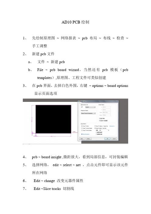
但是⾏业内很多是放置在Keep Out Layer,多数板⼚也是把Keep Out Layer作为边框直接裁掉。
2.布线外围框画在Keep Out Layer(放置-⾛线)。
画完板把它删掉,以免做板被裁掉。
3.固定孔画在机械层(放置-圆环)。
但是和板框⼀样,⾏业内很多是放置在Keep Out Layer。
但⽤3D看时看不到孔,做出板时是有孔的。
----软件缺陷如需3D效果下看到孔,直接放置⼀个焊盘,层为Multi,如外形尺⼨为1.0mm,把通孔尺⼨改成更⼤如1.2mm。
4.固定孔也可以在顶层放置⼀个过孔,将孔尺⼨和孔直径都改成⼀样⼤⼩,改属性始层为Top Layer,改属性末层为Bottom Layer。
这样3D下可以看见孔,但是孔为⾦属过孔。
5.在PCB编辑模式下,按3键转换为3D预览模式,按2键转换为2D预览模式。
3D预览模式下按住Ctrl然后滚动滚轮可以缩放;3D预览模式下按住Shift然后按住右键拖动⿏标可以旋转。
6.画PCB封装,先放置⼀个焊盘,然后编辑-设置参考-定位,可以将焊盘的坐标都归零,然后再放第⼆个焊盘并调整其坐标值,就可以准确定位焊盘距离。
7.画PCB封装,放置焊盘—双击焊盘,可设置焊盘形状(外形),孔⼤⼩(贴⽚就将通孔尺⼨改为0),标识,层(贴⽚就设置层为Top Layer,插件就设置层为Multi Layer,单层板插件也设置层为Multi Layer)。
顶层圆底层⽅的焊盘,将尺⼨和外形由选项(简单)改为(顶层-中间层-底层),并修改顶层或底层的外形。
按3键进⾏3D预览。
8.PCB板⼦按1:1⽐例打出来。
⽂件-页⾯设计9.放置⽹络标号必须要有电⽓连接,也就是放置时必须要出现红叉。
10. 覆铜需要与焊盘完全融合的设置⽅法,将覆铜时候焊盘设置成全部连接,⽽⾮热焊盘连接,规则设置如下所⽰:设计---规则---plane---polygon connect style---polygonconnect 关联类型选择下图11.对于⼀些可以忽略的错误,可以点击⼯具--复位错误标志,就可以消除了,但是当你再动这两个元件时⼜会显⽰绿⾊,所以最好等元件布局OK了再进⾏此操作。
marvelousdesigner10使用教程及快捷键

marvelousdesigner10使用教程及快捷键1、下载并进行解压即可得到Marvelous Designer 10安装包和crack补丁;2、双击“MarvelousDesigner10_Personal_6_0_351_Installer_x64.exe”依提示进行安装;3、选择软件安装路径,默认即可;4、等待软件安装完成,点击finish退出引导,先不要启动软件;5、将crack补丁复制到软件安装路径下替换;【默认路径C:\Program Files\Marvelous Designer 10 Personal】6、双击运行软件,这里需要登录Marvelous Designer账号,没有的用户可以点击sign up注册一个;7、登录完成后,设置语言为简体中文,然后点击ok;8、至此,Marvelous Designer 10中文破解版软件成功破解,到期时间为无限制。
H 连点成面Z 编辑点线N 缝合ctrl + K 冻结/解冻ctrl + B reverse sewspace 模拟shift 得到约束条件ctrl+G 翻转面片Ctrl+H 硬化一、基础设置1、语言设置2、操作习惯设置3、单位 /字体设置4、三角 /四边面设置5、坐标设置二、编辑1、反转缝合线:Ctrl+B2、充气:流程1)框选要充气得板片2)在属性面板压力选项输入数值3)选择3D视图后按空格键模拟运算。
3、反转面片:Ctrl+G(选择模型右键选择“表面反转”)4、硬化:Ctrl+H(有点像把布料硬转化成柔软橡胶,利于拉扯调形,再次使用取消硬化)5、冻结板片:Ctrl+K(选择板片右键选择【冷冻】)被冻结的板片不会参与模拟运算。
6、约束收缩:7、模型面数细分:选择板片,在其属性面板中调节【粒子间距】的数值(数值越大,面数越少)。
三、常见问题1、硬化的那个用来拉扯的抓手怎么调出来?按A键,切换到调整板片工具就有了2、怎么旋转视图?把操作习惯设为Maya之后,按住Alt不放+按鼠标左键不放,并移动鼠标。
AD10 快捷键

Environment ShortcutsModified by Phil Loughhead on 19-Mar-2014Parent article:Shortcut KeysF1Access Documentation Library (in context with object under cursor) CTRL + O Access Choose Document to Open dialogCTRL + F4Close active documentCTRL + S Save current documentCTRL + P Print current documentALT + F4Close Altium DesignerCTRL + TAB Cycle through open documents (to the right). Alternatively, enable the Ctrl+Tab switches to the last active document option on the System -View page of the Preferences dialog.SHIFT + CTRL + TAB Cycle through open documents (to the left). Alternatively, enablethe Ctrl+Tab switches to the last active document option on the System -View page of the Preferences dialog.Drag & drop fromWindows Explorer intoAltium DesignerOpen document as a free documentF4Hide/display all floating panelsSHIFT + F4Tile open documentsSHIFT + F5Toggle between active panel and workspace ALT + F5Toggle full screen mode on/offHold CTRL while movinga panelPrevent automatic docking, grouping or snapping Source URL: /display/ADRR/Environment+ShortcutsProject ShortcutsModified by Phil Loughhead on 19-Mar-2014Parent article:Shortcut KeysC, C Compile the current design projectC, D Compile DocumentC, O Open the Options for Project dialog for the current projectCTRL + ALT + O Access the Open Project Documents dialog for the current project C, L Close all documents belonging to active projectC, T, M Access Storage Manager panelC, T, L Access Local History for the current projectC, P Access the Project Packager wizardSource URL: /display/ADRR/Project+ShortcutsPanel ShortcutsModified by Phil Loughhead on 19-Mar-2014Parent article:Shortcut KeysCommon Panel ShortcutsHOME Jump to first entry in panelEND Jump to last entry in panel↑Move to previous entry in the panel↓Move to next entry in the panel←Collapse expanded top-level entry or sub-folder→Expand collapsed top-level entry or sub-folderLeft-click Select entry under cursorRight-click Display context sensitive pop-up menuLeft-click on a columnheaderSort data by that columnLeft-click & drag columnheaderMove data columnLeft-click and type Direct filtering based on typed character(s)ESC Clear current filtering when using direct filter featureBACKSPACE Clear previously entered filter characters when using direct filter featureProjects Panel ShortcutsDouble Left-click Edit document under cursorDrag & drop from one project to another Move selected documentCTRL + Drag & drop from one project to another Link selected document into second project CAM Panel ShortcutsSelect layer, ←Turn all layers OFF except selected oneSelect layer, →Turn all layers ONDouble Left-click on a layer Make that layer the current layerSelect two layers, C Access Compare Layers dialogSelect layer, DELETE Delete layerList Panel Shortcuts↑ ↓ ← →SHIFT focus to next cell in direction of arrow keyLeft-click & drag Multi-select in direction of mouse movementCTRL + Click Multi-select (non-sequential)SHIFT + Click Multi-select (sequential)SPACEBAR (Schematic)Edit selected cellSPACEBAR (PCB)Flush current entry for cell currently being editedF2Edit selected cellENTER (Schematic)Finish editing current cellENTER (PCB)Finish editing current cell and enter edit mode for cell beneath CTRL + C (or CTRL + INSERT)CopyCTRL + V (or SHIFT + INSERT)PastePAGE UP Jump selection to top of visible list areaPAGE DOWN Jump selection to bottom of visible list areaMouse-wheel Pan up or downSource URL: /display/ADRR/Panel+ShortcutsCommon Schematic & PCB Editor ShortcutsModified by Phil Loughhead on 19-Mar-2014Parent article:Shortcut KeysCommon Schematic and PCB Editor ShortcutsSHIFT While autopanning to pan at higher speedY While placing an object to flip it along the Y-axisX While placing an object to flip it along the X-axis↑ ↓ ← →Move cursor one grid increment in direction of arrow key SHIFT + ↑ ↓ ← →Move cursor ten grid increments in direction of arrow key CTRL + ↑ ↓ ← →Move selection one grid increment in direction of arrow key CTRL + SHIFT + ↑ ↓ ← →Move selection ten grid increments in direction of arrow key ESC Escape from current processEND Redraw the screenHOME Redraw screen with center at the cursor pointCTRL + HOME Jump to absolute origin (lower left corner of workspace) CTRL + Mouse-wheel down (orPAGE DOWN)Zoom outCTRL + Mouse-wheel up (or PAGE UP)Zoom in around cursor (zooms around cursor, position the cursor first)Mouse-wheel Pan up/downSHIFT + Mouse-wheel Pan left/rightA Display Align sub-menuB Display Toolbars sub-menuJ Display Jump sub-menuK Display Workspace Panels sub-menu M Display Move sub-menuO Pop-up right-click Options menuS Display Select sub-menuX Display DeSelect sub-menuZ Pop-up menu with zoom commands CTRL + Z UndoCTRL + Y RedoCTRL + A Select all CTRL + C (or CTRL + INSERT)Copy CTRL + X (or SHIFT + DELETE)Cut CTRL + V (or SHIFT + INSERT)PasteCTRL + R Copy to clipboard and repeat paste selected objects (Rubber Stamp)CTRL + R then ESC Re-enters Rubber Stamp mode using the current clipboard contentCTRL + Q Access the Selection Memory dialogALT Constrain object movement horizontally or vertically DELETE Delete selectionV, D View documentV, F View fit placed objectsX, A De-select allRight-click & hold Display slider hand & slide viewCTRL + Right-click & hold +Move mouse up/downDisplay zoom cursor and zoom in/outLeft-click Select/deselect object under cursorRight-click Pop-up floating menu, or escape from current operation Right-click on object, select FindSimilarLoad object under cursor into Find Similar Objects dialogLeft-click, hold & drag (in freespace)Select inside areaLeft-click & hold Move object/selection under cursorLeft Double-click Edit objectSHIFT + Left-click Add/remove object from selection setTAB Edit attributes while placing (cursor must be placing or moving an object)SHIFT + C Clear current FilterSHIFT + F Click on object to display Find Similar Objects dialog Y Pop-up Quick Queries menuF11Toggle Inspector panel on/offF12Toggle Filter panel on/offSHIFT + F12Toggle List panel on/offALT + F5Toggle full screen mode, Left-click Cross probe to matching object on target document, stay remaining in source document, CTRL + Left-click Cross probe and jump to matching object on target, jumping to target documentSHIFT + CTRL + T Align selected objects by top edgesSHIFT + CTRL + L Align selected objects by left edgesSHIFT + CTRL + R Align selected objects by right edgesSHIFT + CTRL + B Align selected objects by bottom edgesSHIFT + CTRL + H Distribute selected objects equally in horizontal plane SHIFT + CTRL + V Distribute selected objects equally in vertical plane SHIFT + CTRL + D Align selected objects to gridCTRL + n (n=1 to 8)Store current selection in memory location nALT + n (n=1 to 8)Recall selection from memory location nSHIFT + n (n=1 to 8)Add current selection to selection already stored in memory location nSHIFT + ALT + n (n=1 to 8)Recall selection from memory location n and add it to current selection in workspaceSHIFT + CTRL + n (n=1 to 8)Apply filtering based on selection set in memory location n. Source URL: /display/ADRR/Common+Schematic+&+PCB+Editor+ShortcutsSchematic Editor ShortcutsModified by Phil Loughhead on 19-Mar-2014Parent article:Shortcut KeysSchematic Editor ShortcutsG Cycle through snap grid settingsF2Edit in-placeCTRL + PAGE DOWN Fit all objects into viewSPACEBAR Rotate counterclockwise by 90 degrees while moving an objectSPACEBAR Toggle start/end mode while placing a wire/bus/line , SPACEBAR Toggle pen color while using highlighting pensSHIFT + SPACEBAR Rotate clockwise by 90 degrees while moving an objectSHIFT + SPACEBAR Cycle Step through placement modes while placing a wire/bus/lineCTRL + SPACEBAR Rotate counterclockwise by 90 degrees while dragging an objectSHIFT + CTRL + SPACEBAR Rotate clockwise by 90 degrees while dragging an object, CTRL + Left-click onHighlight connection/net on target sheet while using highlighting pens port or sheet entrySHIFT + CTRL + C Clear all highlighting applied by highlighting pensBACKSPACE Remove the last vertex when placing a wire/bus/line/polygonLeft-click, hold + DELETE When a wire is selected to delete a vertexLeft-click, hold + INSERT When a wire is selected to add a vertexCTRL + Left-click & drag Drag objectLeft-click in Navigator panel Cross probe to object on schematic documentALT + Left-click in NavigatorCross probe to object on both schematic document and PCBpanelALT + Left-click on netHighlight all elements in net on sheetobjectCTRL + Double Left-click On sheet symbol to descend hierarchyCTRL + Double Left-click On port to ascend hierarchy+ (numeric keypad)Enlarge IEEE symbol size during placement or movement- (numeric keypad)Reduce IEEE symbol size during placement or movementCTRL + F Find textCTRL + H Find and replace textF3Find next occurrence of searched textINSERT Copy attributes of object under the cursor while placing an object of the same typeS Swap sheet entry side while moving one or more selected sheet entriesV Reverse sheet entry order while moving two or more selected sheet entriesT Toggle sheet entry IO type while moving one or more selected sheet entriesT Toggle all sheet entry IO types while resizing selected sheet symbol T, P Access Schematic - General page of Preferences dialogSource URL: /display/ADRR/Schematic+Editor+ShortcutsPCB Editor ShortcutsModified by Phil Loughhead on 19-Mar-2014Parent article:Shortcut KeysPCB Editor ShortcutsSHIFT + R Cycle through three routing modes (ignore, avoid or push obstacle) SHIFT + E Toggle electrical grid on/offSHIFT + B Build QuerySHIFT + PAGE UP Zoom-in in small incrementsSHIFT + PAGE DOWN Zoom-out in small incrementsCTRL + PAGE UP Zoom-in to 400%CTRL + PAGE DOWN Fit document into viewCTRL + END Jump to defined relative origin for the workspaceALT + END Redraw current layer onlyALT + INSERT Paste on current layerCTRL + G Pop up Snap Grid dialogG Pop up Snap Grid menuN Hide the ratsnest while moving a componentL Flip component being moved to other side of boardSHIFT + F1Pressed while routing, displays the appropriate interactive routing shortcut keysTAB Pressed while routing, length tuning, component or string placement displays appropriate interactive editing dialogF2Display Board Insight and Heads Up display optionsCTRL + Left-click Highlight routed net under cursor (repeat in free space to clear) CTRL + SPACEBAR Cycle through connection lines modes during interactive routing BACKSPACE Remove last track corner during interactive routingSHIFT + S Toggle single layer mode on/off (or cycle through Single Layer Modes set in PCB Preferences: Board Insight Display)O, D, D, O, ENTER Set all primitives to display in draft modeO, D, F, O, ENTER Set all primitives to display in final modeO, D (or CTRL + D)Access Show/Hide page of View Configurations dialogL Access Board Layers And Colors page of View Configurations dialogCTRL + H Select connected copperCTRL + SHIFT + Left-click &holdBreak trackSHIFT + CTRL + Left-click Highlight additional routed net under cursor + (numeric keypad)Next layer- (numeric keypad)Previous layerCTRL + Click Highlights layer content on layer tabs CTRL + SHIFT + Click Increments highlighting on layer tabs CTRL + ALT + Mouse Hovers highlight layer on layer tabs* (numeric keypad)Next routing layerM Display Move sub-menuALT Hold to temporarily switch from avoid-obstacle to ignore-obstacle modeCTRL Hold to temporarily disable electrical grid while routing CTRL + M Measure distanceSPACEBAR (in interactive process)Rotate object anti-clockwise (define rotation step on PCB Editor -General page of Preferences dialog)SPACEBAR (duringinteractive routing)Toggle start/end modeSHIFT + SPACEBAR (ininteractive process)Rotate object being moved clockwiseSHIFT + SPACEBAR (duringinteractive routing)Step through corner modes during interactive routing [Decrease mask level for permanent filter]Increase mask level for permanent filterALT ←View previous component for active library documentALT →View next component for active library documentQ Toggle units (metric/imperial)Ctrl + Q Toggle units (metric/imperial) within an open PCB Editor dialog T, B Access 3D Body Manager dialogT, P Access Preferences dialogBACKSPACE Remove last interactive length tuning segmentSPACEBAR Next interactive length tuning wave patternSHIFT + SPACEBAR Previous interactive length tuning tuning patternSHIFT + R Toggle Routing Mode, (comma)Decrease interactive length tuning pattern amplitude by one increment. (full stop / period)Increase interactive length tuning pattern amplitude by one increment1Decrease interactive length tuning miter or radius2Increase interactive length tuning miter or radius3Decrease interactive length tuning pattern gap by increment 4Increase interactive length tuning pattern gap by increment Y Toggle interactive length tuning amplitude direction Interactive Routing ShortcutsShift+F1 (or ~ (tilde))Display list of shortcutsCTRLAuto-complete segments to target+ ClickBACKSPACE Remove last segmentESC Terminate current traceSHIFTAdd accordion sections (interactive length tuning)+ ASHIFTToggle auto-complete+ CSHIFTToggle length tuning gauge+ GSHIFTToggle visible routing area+ OSHIFTToggle Push mode+ PSHIFTToggle glossing+ QSHIFTToggle routing mode+ RSHIFTSwitch layer for current trace+ SSHIFTSelect favorite via size+ VSHIFTOpen Choose Favorite Width dialog.+ W, (comma)Decrease arc setbackSHIFTDecrease arc setback 10x+ . (comma). (full stop / period)Increase arc setbackSHIFTIncrease arc setback 10x+ . (full stop / period)ENTER Place Segment+ (plus)Next Layer (numeric keypad)- (minus)Previous Layer (numeric keypad)* (multiply)Next Signal Layer (numeric keypad)SPACEBAR Cycle corner directionSHIFT+ SPACEBARCycle corner styles (if restrict to 90/45° is not enabled) TAB Edit trace properties1Toggle Look-ahead Mode – Switches between 1 and 2 segment placement mode2Add via, no layer changeSHIFT + 2Add fanout via, tool immediately waits for next fanout to route and via to place3Cycle track width source4Cycle via size source6Force walk-around (with key pressed)7Switch leader trace or switch routing target in single trace mode 8Toggle dynamic routing mode9Switches to opposite routing pointInteractive Differential Pair Routing ShortcutsShift+F1 (or ~ (tilde))Display list of shortcutsCTRL+ ClickCommit auto complete segments (if applicable) BACKSPACE Remove last segmentSHIFT+ BACKSPACERemove last cluster of segmentsESC Terminate current traceSHIFT+ RToggle routing modeSHIFT+ WOpen Choose Favorite Width dialog.ENTER Place segment+ (plus)Next layer- (minus)Previous layer* (multiply)Next signal layerSPACEBAR Toggle corner directionSHIFT+ SPACEBARCycle corner styles (if restrict to 90/45° is not enabled)TAB Edit trace properties3Cycle track width source4Cycle via size source5Toggle Auto-complete6Change via modeInteractive Length Tuning ShortcutsShift+F1 (or ~ (tilde))Display list of shortcutsTAB Edit tuning pattern settingsBACKSPACE Remove last segmentSPACEBAR Next tuning patternSHIFTPrevious tuning pattern+ SPACEBARSHIFTToggle Routing Mode+ R, (comma)Decrease pattern amplitude by one increment . (full stop / period)Increase pattern amplitude by one increment 1Decrease miter or radius2Increase miter or radius3Decrease pattern gap by increment4Increase pattern gap by incrementY Toggle amplitude directionSource URL: /display/ADRR/PCB+Editor+Shortcuts3D Layout Mode Shortcuts Modified by Phil Loughhead on 19-Mar-2014 Parent article:Shortcut Keys3D Visualization Shortcuts0Rotates the 3D view so that the camera perspective is perpendicular to the board and will rotate the board so that the horizontal plane (X-axis) runs along the bottom of the editing window (at 0° rotation)9Rotates the 3D view so that the camera perspective is perpendicular to the board and will rotate the board so that the horizontal plane (X-axis) runs along the right side of the editing window (at 90° rotation)2From 3D switches to 2D using last used 2D view configuration 3From 2D switches to 3D using last used 3D view configurationSHIFT Turns on 3D rotational movement sphere (left-click and drag from sphere evblements to rotate model)V, F Fit boardV, B Flip board horizontally about cursor positionMouse-wheel Pan up/downSHIFT + Mouse-wheel Pan left/rightCTRL + Mouse-wheel Zoom in/out incrementallyCTRL + Right drag Zoom in/out smoothlyCTRL + C Create clipboard bitmap (.bmp) image of current 3D viewPAGE UP / PAGEDOWNZoom in/out incrementallyT, P Access PCB Editor - Display page of Preferences dialogL Access Physical Materials (3D) page of View Configurations dialog 3D Body Placement Shortcuts+ (plus)Next layer- (minus)previous layerL Flip 3D body to paired mechanical layerX Flip 3D body around X-axisY Flip 3D body around Y-axisSPACEBAR Rotate 3D body counter-clockwiseSHIFT + SPACEBAR Rotate 3D body clockwise2Rotate 3D body counter-clockwise around it's X-axis3Decrease 3D body standoff height (Z-axis) by one Snap Grid increment 4Rotate 3D body counter-clockwise around it's Y-axis6Rotate 3D body clockwise around it's Y-axis8Rotate 3D body clockwise around it's X-axis9Decrease 3D body standoff height (Z-axis) by one Snap Grid increment ¬ (left arrow)Move 3D body left along X-axis by one Snap Grid incrementSHIFT + ¬ (left arrow)Move 3D body left along X-axis by 10x Snap Grid increment® (right arrow)Move 3D body right along X-axis by one Snap Grid incrementSHIFT + ® (right arrow)Move 3D body right along X-axis by 10x Snap Grid increment(up arrow)Move 3D body backward along Y-axis by one Snap Grid increment SHIFT + (up arrow)Move 3D body forward along Y-axis by 10x Snap Grid increment¯ (down arrow)Move 3D body forward along Y-axis by one Snap Grid increment SHIFT + ¯ (down arrow)Move 3D body forward along Y-axis by 10x Snap Grid incrementSource URL: /display/ADRR/3D+Layout+Mode+ShortcutsOutput Job Editor ShortcutsModified by Phil Loughhead on 19-Mar-2014Parent article:Shortcut KeysOutput Job Editor ShortcutsCTRL + X (or SHIFT + DELETE)CutCTRL + C (or CTRL + INSERT)CopyCTRL + V (or SHIFT + INSERT)PasteCTRL + D DuplicateDELETE ClearALT + ENTER ConfigureCTRL + F9Run Focused Output GeneratorSHIFT + CTRL + F9Run Selected Output GeneratorsF9Run all Batch-enabled Output Generators SHIFT + CTRL + O Access Output Job Options dialogSource URL: /display/ADRR/Output+Job+Editor+ShortcutsCAM Editor ShortcutsModified by Phil Loughhead on 19-Mar-2014Parent article:Shortcut KeysCAM Editor (CAMtastic®) ShortcutsCTRL + Z (or ALT + BACKSPACE)UndoCTRL + Y (or CTRL + BACKSPACE)RedoCTRL + X CutCTRL + C (or CTRL + INSERT)CopyCTRL + V (or SHIFT + INSERT)PasteCTRL + E ClearCTRL + M MirrorCTRL + R RotateCTRL + L Align SelectiveL Merge LayersALT + C Select using crossing windowALT + P Select previous selectionCTRL + F Toggle Flash selection mode On/Off CTRL + T Toggle Trace selection mode On/Off CTRL + A Array objectsCTRL + D Modify/change objectsCTRL + I Set originCTRL + U Scale objectsHOME View allSHIFT + P View around specified pointCTRL + Mouse-wheel up (or PAGE UP)Zoom inCTRL + Mouse-wheel down (or PAGE DOWN)Zoom outMouse-wheel up Pan upMouse-wheel down Pan downSHIFT + Mouse-wheel up Pan leftSHIFT + Mouse-wheel down Pan rightSHIFT + V Zoom lastEND RefreshD Dynamic panning modeSHIFT + B View Film BoxCTRL + HOME Zoom Film BoxALT + HOME Zoom current DCodeSHIFT + E Toggle view of Extents Box On/Off SHIFT + F Toggle Fill Mode On/OffSHIFT + H Toggle highlight of current objects using current D codeN Toggle negative view SHIFT + T Toggle translucent viewSHIFT + G Access CAM Editor - Drawing Modes page of Preferences dialogQ Query objectSHIFT + N Query netSHIFT + M Measure point-to-pointSHIFT + A Access apertures tableK Access Set Layers Off dialogALT + K Access Set Layers On dialog SHIFT + S Toggle Object Snap modeESC Cancel actionSHIFT + CTRL + R Repeat last action+ (numeric keypad)Display next layer only- (numeric keypad)Display previous layer only* (numeric keypad)Display next signal/plane layer only Source URL: /display/ADRR/CAM+Editor+ShortcutsDevices View ShortcutsModified by Phil Loughhead on 19-Mar-2014Parent article:Shortcut KeysDevices View ShortcutsF5Refresh allESC HALT Process FlowCTRL + F9Compile Bit FileCTRL + F10Rebuild Bit FileF12Reset Hard DeviceF9Compile Bit File and DownloadF10Rebuild Bit File and DownloadF11Download Bit FileSHIFT + CTRL + F9Compile All Bit FilesSHIFT + CTRL + F10Rebuild All Bit FilesSHIFT + F12Reset All DevicesSHIFT + F9Compile All Bit Files and DownloadSHIFT + F10Rebuild All Bit Files and DownloadSHIFT + F11Download All Bit FilesALT + T, P Access FPGA - Devices View page of Preferences dialog Source URL: /display/ADRR/Devices+View+ShortcutsWaveform Editor ShortcutsModified by Phil Loughhead on 19-Mar-2014Parent article:Shortcut KeysDigital Waveform Editor ShortcutsPAGE UP Zoom in around active time cursorPAGE DOWN Zoom out around active time cursorCTRL + PAGE DOWN Fit documentCTRL + A Select all waveformsCTRL + C (or CTRL + INSERT)Copy waveformCTRL + X (or SHIFT + DELETE)Cut waveformCTRL + V (or SHIFT + INSERT)Paste waveformLeft-click & drag Relocate focused waveformJ Display Jump sub-menuSHIFT + CTRL + F Jump to first transition for focused waveform SHIFT + CTRL + N Jump to next transition for focused waveform SHIFT + CTRL + P Jump to previous transition for focused waveform SHIFT + CTRL + L Jump to last transition for focused waveformT, P Access Preferences dialogSimData Editor ShortcutsCTRL + X (or SHIFT + DELETE)CutCTRL + C CopyCTRL + V (or SHIFT + INSERT)PasteDELETE Clear+ (numeric keypad)Next chart- (numeric keypad)Previous chartPAGE UP Zoom inPAGE DOWN Zoom outCTRL + PAGE DOWN Fit documentEND RefreshESC (or SHIFT + C)Clear filter↑ ↓Scroll through chart, one wave plot at a time in direction of arrow SHIFT + ↑Scroll upwards through chart, one page at a timeCTRL + ↑ (or CTRL + HOME)Jump to top of chartSHIFT + ↓Scroll downwards through chart, one page at a timeCTRL + ↓ (or CTRL + END)Jump to bottom of chart← →Scroll through chart, one major division on X-axis at a time in direction of arrowSHIFT + ←Scroll left through chart, one page at a time CTRL + ←Jump to start of X-axisSHIFT + →Scroll right through chart, one page at a time CTRL + →Jump to end of X-axisSource URL: /display/ADRR/Waveform+Editor+Shortcuts。
altium designer常用快捷键总结

altium designer常用快捷键总结Altium Designer是一款功能强大的电子设计自动化(EDA)软件,它在电路设计、PCB布局和制造准备方面提供了全面的解决方案。
这款软件的高效与便利离不开一系列的快捷键操作,今天我们就来总结一下Altium Designer中常用的快捷键。
在本篇文章中,我们将按照主题一步一步解答,帮助读者更好地理解和掌握这些快捷键。
一、必备的基本操作快捷键(500字)开始之前,让我们先了解几个非常基本且常用的快捷键,这些快捷键可以帮助你更快捷地进行常规操作。
1. 新建文件:Ctrl + N2. 打开文件:Ctrl + O3. 保存文件:Ctrl + S4. 撤销操作:Ctrl + Z5. 重做操作:Ctrl + Y6. 复制选择:Ctrl + C7. 剪切选择:Ctrl + X8. 粘贴选择:Ctrl + V9. 删除选择:Delete10. 全选:Ctrl + A11. 退出软件:Alt + F4这些快捷键可以帮助你更高效地进行文件管理和常规操作,熟练掌握它们将极大地提高你的工作效率。
二、器件选择与放置快捷键(500字)在电路设计中,选择和放置器件是最基本的操作之一。
Altium Designer 提供了一系列的快捷键来帮助你更迅速地完成这些操作。
1. 选择下一个器件:Tab2. 选择上一个器件:Shift + Tab3. 向上移动器件:Up Arrow4. 向下移动器件:Down Arrow5. 向左移动器件:Left Arrow6. 向右移动器件:Right Arrow7. 放置器件:Space8. 放置器件并旋转:Ctrl + Space9. 删除选择的器件:Delete10. 复制选择的器件:Ctrl + Shift + C11. 移动器件:M这些快捷键可以大大简化器件的选择、放置、移动和复制过程,使你能够更高效地进行电路设计。
三、布线和连接快捷键(500字)在完成电路的布线和连接之后,我们需要进行一系列的调整和优化。
AD10快捷键.

Altium designer快捷键发表于:2014年12月9日星期二雪域天狼L打开层S打开选择J 跳转Q 英寸和毫米选择空格翻转选择某物体(导线,过孔等),同时按下Tab键可改变其属性(导线长度,过孔大小等)选择目标,按住shift拖动在PCB电气层之间切换(小键盘上的*)。
在交互布线的过程中,按此键则换层并自动添加过孔。
这很常用。
DXP->preferences 系统设置其中General--Use localized resources 中文其中Backup --设置备份时间树形图标--home快捷键--右下角help-shortcuts默认布局--View-Desktop layouts--Default窗口缩回的速度--DXP->preferences->system->view--Hide delay打开不同面板--右下角System等等切换不同窗口--ctrl+tab放大和缩小---ctrl+鼠标中键滚轴选取工具栏上的图标,下面状态栏有它对应的一些快捷方式用途DeSign-Template-Set Template File Name...A4 修改右下方的边框(title,日期)格式拖动移动时连线跟着自动延长 Drag---ctrl+鼠标拖动复制目标---选择目标,按住shift拖动自动添加元件编号---Tools->Annotate SchematicsPreferences-->Schematic-->Graphical Editing Convert Special Strings 转换特殊字符串原理图出现红色波浪形表示有违法规则的地方(例如两个同名R1)编译完原理图,查看Message窗口(注意元件库导出隐藏的VCC,GND引脚)原理图连接处,或添加NEt,会有四个白色方形小点总线连接总net 例如:RB[0..7] 每一导线net分别为:RB0,RB1....如何全局修改例如:单击电容C1选中,鼠标右键选择Find Similar Objects (Select Matching 选中,二步骤可以跳过(1) Part Comment ---same Current Footprint ---same ,点击OK按钮(2) Select ALL(3) SCH Inspector 窗口修改 FootprintTools-->FootPrint Manager分层设计(1)一种水平设置,N个分图,net设置全局(project-->projectoptions--> Identifier Scope..Gloal) 不推荐(2)一种垂直设置,一个总图(Sheet Entry),N个分图(PORT) 连接只能Sheet Entry到PORT第二种方法:(1)Place sheet Symbol(方框) 和 sheet Entry(放在方框边界内侧)(2)选择sheet Symbol,右键选择"Sheet symbol actions"--creat sheet from symbol原理图库(1) File-->New-->Library-->sch..(2) 右边下方SCH打开SCH Library 窗口(3) Place->RecTangle,注意放在原点(4) Library Components PropertiesDesignator U?Comment max232Symbol Refernece max234(5) 可将一个元件库分为两个Part,例如parta,partb(通过Tools-->new part)特殊用途:选择该元件,按F1打开该元件的pdf文档Library Components Properties-->Parameters for Component -->Add.. Name: HelpURL Value: C:\zy\abc.pdf#page=5PCB库(1) File-->New-->Library-->pcb..(2) 右边下方PCB打开pcb Library 窗口IPC FootPrint wizard..(比较有用)画图要焊盘要比datasheet中长1mm集成库(1) File-->New-->Project-->Interger Library(2) 新建sch.lib和pcb.lib, 在sch.lib中选择Tools-->Model Manage....(3) Project-->Compile Integrated Library盲孔(BIIND VIA):从印制板内仅延展到一个表层的导通孔。
AD10 快捷键

Configuring the 2D Board Insight System Heads Up Display DataBoard Insight Pop-up ModeBoard Insight Panel ModeVisual Pick ListSingle Layer ModeLayer TransparencyActive Layer ControlNet Name Displayed on TracksNet HighlightingLive HighlightingPad and Via Detail Display OptionsLocked Objects Display Options3D Board InsightNotesDisplaying FPGA InformationSee AlsoBoard Insight™ is a configurable system of features that give you complete control over viewing and working with your PCB design.A complex multi-layer board makes for a visually dense and often difficult to interpret workspace. Altium Designer's Board Insight system makes it easier to view and understand the objects in your design. It consists of an integrated set of features developed to meet your view management needs.2D Board Insight includes:Insight LenInsight PanelInsight Pop-upHeads Up Display cursor informationFloating graphical viewsEnhanced Single Layer modeEnhanced labeling on objectsIntegrated with Board Insight are enhanced Single Layer mode and 3D visualization features. In Single Layer mode you can see clearly what is on a given layer, but also have perspective as to what is on other layers. With 3D visualization you can see a 3D model or cross-sectional views of your PCB, relevant to cursor position, in a separate panel.Configuring the 2D Board Insight SystemPress F2 to display the Board Insight pop-up menu.PCB Editor - Board Insight Preferences2D Board Insight options are configured in the pages of the dialog. Here you can configure Board Insight options - from hover delays, lens shape and size, through to shortcuts. A quick wayLens Heads Up Displayto access many of the Board Insight features, such as the or , is via shortcut keys. To help you learn the shortcuts, and as an alternate to remembering them, press F2 while you are working. This will open Board Insight Viewthe sub-menu (also accessible via the menu), which you can use as a reference to read ashortcut from, or as a menu to select an entry.The PCB Board Insight Mode preferences.Heads UpIn the column of this dialog, enable each property option you want displayed. Font settings can also be adjusted.Heads Up Display hover mode showing detailed information about objects currently under the cursor.Hover modeIf you pause for a moment as you are moving the cursor, the Heads Up Display will switch to . Extra information is displayed in Hover mode, this can include a summary, available shortcuts, rule violations, net,PCB Editor - Board Insight Modes component and primitive details. Configure the HUD Hover mode in the page of Preferencesthe dialog.Board Insight Pop-up ModeThe Board Insight's Pop-up mode, being used to examine a design violation.The Board Insight system's Pop-up mode is an excellent tool for interrogating objects under the cursor. Pressing SHI FT + X SHIFT + Vor presents the Pop-up mode display, which includes list of all components, nets and violations under the cursor, and a graphical display of the object currently chosen in the list. From the list you can edit, select or zoom on any of the objects. As well as the component, net and violation group-type objects, the Board Insight popup list will include the primitive objects that were under the cursor and belong to them, such as pads and tracks. The list is hierarchical, allowing you, for example, to drill down for complete detail on the objects causing a violation.SHIFT + V SHIFT + Use the shortcut to load the popup with information about violations currently under the cursor.Xloads the popup with information about any nets and components under the cursor.Board Insight Panel ModeBoard InsightThe panel provides the same information as the popup view, in a panel, with no keystrokes required to update the contents (Figure 9). The panel allows you to view in more detail what is in under the cursor. When you hover the cursor over component, net or violation objects, they will be loaded into the panel. Once the information is in the panel it will remain until the cursor is paused in a new location.The top region of the panel displays a graphical preview of the object.The second region lists all primitives under the cursor. Here you can edit them, change their selection state and navigate to them. The available information can include listing components, nets and violations. From the list you can select, edit or zoom in on any of the objects.Show LensThe optional lower region of the panel (toggled via the option) gives you a close up 2D view of the areaThe Board Insight panel gives detailed view of what is currently under the cursor. Visual Pick ListDisplaying net names on the tracks makes it easy to "read" the routing.Net HighlightingA modern PCB can be dense and difficult to interpret.Making sense of a complex PCB design is not easy, with dense component placements, tight routing, and multiple signal layers. Altium Designer includes a number of net highlighting features to help you examine the routing. ToCTRL + Clickhighlight any net on the board, on any net, and everything in the workspace that is not part of that net is faded, making the routing stand out on all signal layers, as shown in the figure below. To highlight multiple nets hold the SHIFT key as you CTRL + Click on each net. CTRL + Click in free space to restore the display, or click the Clearbutton at the bottom right of the workspace.An example of a net being highlighted using CTRL + Click.Live HighlightingNet highlighting can be used dynamically too, meaning that as you move the cursor over a net, it can be highlighted. This method uses an outline highlight, which is configurable, and does not affect the display of the remainder of the PCB. The figure below shows the same net highlighted using Altium Designer's Live Highlighting.An example of a net being highlighted using Live Highlighting.|Live Highlighting configuration options.PCB Editor Board Insight Display Preferences Live HighlightingThe - page of the dialog has controls in the regi on to enable and configure this feature. When enabled, this feature can be limited to highlighting only when the SHIF Tkey is pressed.Pad and Via Detail Display OptionsPad and Via Detail Options.Pad and Via Display Options PCB Editor You can control the display of pad and via details using the region of the- Board Insight Display Preferencespage of the dialog, as shown above. Here you can configure font, color and background for pad and via information. Strings are automatically presented as right-reading, and aligned in theSmart Display Colordirection that maximizes the area available to display them. The option automatically selects a font color to give good contrast so the text can be easily read.Note: Depending on the display mode (DirectX or GDI), not all pad and via detail features will be visible.Locked Objects Display OptionsLocked objects can be highlighted by the Locked Object Texture.Control when the display of locked objects occurs.You can control how locked objects are displayed in the workspace, making them easier to identify visually. Use the Show Locked Texture on Objects PCB Editor - Board Insight Display Pr controls in the region of the page of the eferencesdialog.Note: The Locked Object texture is available in DirectX mode only. Object locking is available using the object's properties.3D Board InsightUse the 3D mode to display the loaded board as if it were assembled.Altium Designer's ability to display the board in 3D greatly enhances your ability to visualize the board as a manufactured and assembled object. There is also a number of Board Insight features that use the 3D mode.The 3D Visualization Panel displays the board in 3D, as well as 2 cross sections of the board.3D VisualizationThe panel displays up to three simultaneous 3D views, including 2 cross-sectional views and a 3D board view, as shown in the figure above. Using this panel you can examine all aspects of your board in 3D, including internal structures, whilst still working on the board in either 2D or 3D mode in the main PCB EditorView»Workspace Panels»PCB»3D Visualization3D window. Open the panel by selecting , or by selecting from the button at the bottom right of Altium Designer.Visualization PCBUse the controls to show/hide the various regions of the panel.To help the designer more intuitively manage programmable devices during the design process, the Board Insight System has been expanded to highlight FPGA component pins and connected routing, based on a user-selectable pin-type property.FPGA pins and connected routing can be colored according to associated FPGA component information.Altium Designer stores valuable FPGA component data which is used during the FPGA and PCB design processes. This information includes I/O bank allocations, I/O pins, clock pins, and differential pair pins. By selecting the Color Overlay Componentappropriate mode in the PCB properties dialog, the component's pads and some of the connected routing will be highlighted in a range of colors, as shown in the figure above.Double-click on a component on the board to set the *Color Overlay* mode.Altium Designer's component libraries are already setup to use this information, the FPGA component detail is looked up in a database based on the component library name, for example XC3S1500-4FG676C. For newNexusDeviceID components, the part can either be named in the same manner, or a parameter called can be added to the schematic component, with the same data. Altium Designer will then be able to look up the new component in its database of FPGA parts.See AlsoBoard Insight FPGA Information demonstration video。
Altium Designer 10快捷键

原理图常用快捷键1 XA取消全选;2 SA全选;3 End刷新;4 ED 删除元件5 EN ,shift+f 全局修改;6 Shift+ctrl+T 上对齐;7 Shift+ctrl+B 下对齐8 Shift+ctrl+L 左对齐9 Shift+ctrl+R 右对齐10 Shift+ctrl+H 左右居中11 Shift+ctrl+V 上下居中12 Ctrl+F 查找原件13 Ctrl+滚动滑轮14 pgup pudn 缩放图纸大小15 PW 放置导线16 VD 整个图纸全屏显示17 VF 所有元件全屏显示18 V A 查看某一部分19 PN 放置网络标号20 FN 新建21 FL全部保存22 TA 元件自动编号23 VS 状态栏的显示隐藏24 TS 在原理图中选中快速切换到pcb中25 Ctrl+S 保存26 VS 下边框显示和隐藏元件库快捷键1 TC 新建元件2 TE 重命名元件3 PP 放置引脚4 PL 划线5 JO 坐标原点6 MB 送到后面7 MV 带到前面PCB库快捷键1 JR 寻找原点2 TC 新建原件3 G 选择距离4 PP 放焊盘PCB常用快捷键1 UA 撤销布线2 Q 公英制转换3 PG 覆铜4 VD 显示全图5 End刷新6 PT 连接导线7 PV 放置过孔8 “*”号切换层9 UC 删除两个焊盘直接的线10 UN 删除整个线的网络11 TE 补泪滴12 G 捕捉距离13 Ctrl+D 显示设置14 Shift+ctrl+T 上对齐15 Shift+ctrl+B 下对齐16 Shift+ctrl+H 左右居中17 Shift+ctrl+V 上下居中18 Shift+ctrl+L 左对齐19 Shift+ctrl+R 右对齐20“-”“+”层的切换21VGV 格,点转换22 EOS 找原点23 Ctrl+M 测量距离24 DSD 切板25 “A”弹出元件排列快捷键26 Shift+Alt+L 元件右对齐27 Shift+Alt+G 元件左对齐28 Shift+Alt+I 元件上对齐29Shift+Alt+N 元件下对齐。
AD10 pcb绘制 原理图技巧
AD10 PCB绘制1、先绘制原理图~ 网络报表~ pcb布局~ 布线~ 检查~手工调整2、新建pcb文件a、文件~ 新建pcbb、File ~ pcb board wizard,当然还有pcb模板(pcbtemplates),原理图、工程文件可类似创建3、在pcb界面,去掉白色外围,右键~ options ~ board options显示页面选项4、pcb ~ board insight ,微距放大,看到局部信息,可封装编辑5、选择网络,edit ~ select ~ net ,点击元件即可显示该元件所在网络6、Edit ~ change 改变元器件属性7、Edit ~Slice tracks 切割线8、View Flip board 水平翻转pcb板,顶层与底层翻转9、Edit ~ align 对齐操作10、Edit ~ origin 设置参考点11、Edit ~ jump 跳转12、Edit ~ find similar objects 查找相似元件,统一修改封装13、Edit ~ refresh 更新14、Pcb ~ 3D可视化三个角度查看pcb板15、View ~ toggle units ,切换单位英制~米制16、Design ~ rules 规则设计pcb规则17、Design ~ board shape pcb 板外形设计a、redefine board shape 重新定义pcb的外形b、move board shape 移动pcb板18、Design ~ layer stack manger 层堆积管理器19、board ~ layers Pcb 板的管理设计20、生产pcb 元件库,design ~ make pcb library ,生产pcb元件库21、Tool ~ design rule check ,设计规则检查,对pcb板进行检查22、Tool ~ Browse violations ,浏览规则检查23、Tool ~ manage 3 D bodies…. 管理3D模型24、Tool ~ un-route 拆除布线,或者网络25、Tool ~ density map 图密度查看pcb布线密度26、Tool ~ re-annotate 重新标号、注释27、Tool ~ 从pcb库更新,库文件元件封装有改动,更新至pcb板28、Tool ~ cross probe 交叉探针,用于pcb图元件封装图与原理图切换29、Tool ~ teardrops 泪滴,增强导线与焊盘的连接性,30、Tool ~ preference 参数设置31、不同层之间的切换,ctrl+shift+滑轮32、Reports ~ measure primitives ,测量某一元件或导线的长度33、Report ~ measure selected objects ,先选中物体,进行测量34、从原理图导入pcb,一般由于以下两点导致无法成功a、某一元件无封装b、对应的封装库未导入35、层的概念a、Top Layer 顶层b、Bottom Layer 底层c、Mechanical 机械层d、Top overlay 顶层丝印层e、Bottom overlay 底层丝印层f、Top paste 顶层焊接层g、Bottom paste 底层焊接层h、TOP/BOTTOM SOLDER(顶层/底层阻焊绿油层):顶层/底层敷设阻焊绿油,以防止铜箔上锡,保持绝缘。
- 1、下载文档前请自行甄别文档内容的完整性,平台不提供额外的编辑、内容补充、找答案等附加服务。
- 2、"仅部分预览"的文档,不可在线预览部分如存在完整性等问题,可反馈申请退款(可完整预览的文档不适用该条件!)。
- 3、如文档侵犯您的权益,请联系客服反馈,我们会尽快为您处理(人工客服工作时间:9:00-18:30)。
ALITUM10快捷键
1、设计浏览器快捷键:
鼠标左击选择鼠标位置的文档
鼠标双击编辑鼠标位置的文档
鼠标右击显示相关的弹出菜单
Ctrl+F4 关闭当前文档
Ctrl+Tab 循环切换所打开的文档
Alt+F4 关闭设计浏览器DXP
2、原理图和PCB通用快捷键:
Shift 当自动平移时,快速平移
Y 放置元件时,上下翻转
X 放置元件时,左右翻转
Shift+↑↓←→箭头方向以十个网格为增量,移动光标
↑↓←→箭头方向以一个网格为增量,移动光标
SpaceBar 放弃屏幕刷新
Esc 退出当前命令
End 屏幕刷新
Home 以光标为中心刷新屏幕
PageDown,Ctrl+鼠标滚轮以光标为中心缩小画面
PageUp, Ctrl+鼠标滚轮以光标为中心防大画面
鼠标滚轮上下移动画面
Shift+鼠标滚轮左右移动画面
Ctrl+Z 撤销上一次操作
Ctrl+Y 重复上一次操作
Ctrl+A 选择全部
Ctrl+S 保存当前文档
Ctrl+C 复制
Ctrl+X 剪切
Ctrl+V 粘贴
Ctrl+R 复制并重复粘贴选中的对象
Delete 删除
V+D 显示整个文档
V+F 显示所有对象
X+A 取消所有选中的对象
单击并按住鼠标右键显示滑动小手并移动画面
点击鼠标左键选择对象
点击鼠标右键显示弹出菜单,或取消当前命令
右击鼠标并选择Find Similar 选择相同对象
点击鼠标左键并按住拖动选择区域内部对象
点击并按住鼠标左键选择光标所在的对象并移动
双击鼠标左键编辑对象
Shift+点击鼠标左键选择或取消选择
TAB 编辑正在放置对象的属性
Shift+C 清除当前过滤的对象
Shift+F 可选择与之相同的对象
Y 弹出快速查询菜单
F11 打开或关闭Inspector面板
F12 打开或关闭List面板
3、原理图快捷键:
Alt 在水平和垂直线上限制对象移动
G 循环切换捕捉网格设置
空格键(Spacebar) 放置对象时旋转90度
空格键(Spacebar) 放置电线、总线、多边形线时激活开始/结束模式
Shift+空格键(Spacebar) 放置电线、总线、多边形线时切换放置模式
退格建(Backspace) 放置电线、总线、多边形线时删除最后一个拐角
点击并按住鼠标左键+Delete 删除所选中线的拐角
点击并按住鼠标左键+Insert 在选中的线处增加拐角
Ctrl+点击并拖动鼠标左键拖动选中的对象
4、PCB快捷键:
Shift+R 切换三种布线模式
Shift+E 打开或关闭电气网格
Ctrl+G 弹出捕获网格对话框
G 弹出捕获网格菜单
N 移动元件时隐藏网状线
L 镜像元件到另一布局层
退格键在布铜线时删除最后一个拐角
Shift+空格键在布铜线时切换拐角模式
空格键布铜线时改变开始/结束模式
Shift+S 切换打开/关闭单层显示模式
O+D+D+Enter 选择草图显示模式
O+D+F+Enter 选择正常显示模式
O+D 显示/隐藏Prefences对话框
L 显示Board Layers对话框
Ctrl+H 选择连接铜线
Ctrl+Shift+Left-Click 打断线
+ 切换到下一层(数字键盘)
- 切换到上一层(数字键盘)
* 下一布线层(数字键盘)
M+V 移动分割平面层顶点
Alt 避开障碍物和忽略障碍物之间切换
Ctrl 布线时临时不显示电气网格
Ctrl+M 测量距离
Shift+空格键顺时针旋转移动的对象
空格键逆时针旋转移动的对象
Q 米制和英制之间的单位切换。