NXP芯片选型手册
NXP DS-LPC1850系统核心板硬件手册
LPC1850 OEM核心板参数概述电子产品市场瞬息万变,对产品开发提出更高的要求,更短的研发周期,更稳定的产品质量,更少的研发投入。
传统芯片级的设计模式,软件编程起始于芯片的寄存器,需要投入大量的资金、人员和时间才有可能构建一个稳定的产品平台。
使用成熟的OEM系统核心板,可以大大减少投入,缩短研发时间,在最短的时间内最到稳定的产品,最大程度规避研发风险。
DS-LPC1850系统核心板在硬件上集成了MCU、NOR Flash、NAND Flash、SDRAM、Clock,构成了一个完整的最小系统。
软件上,提供开源操作系统、完整的外设驱动源码,并以静态连接库形式提供稳定的中间件,包括TCP/IP网络协议栈、GUI图形用户界面库、FA T文件系统、USB标准类库,为开发者提供一个稳定的开发平台。
使用系统核心板开发产品,进行产品硬件设计时,您只要关注产品特有的一些硬件接口,而在产品软件开发时,您只要关注真正与用户相关的业务逻辑。
只有将注意力真正放在与产品的用户特性上,才能迅速开发出符合市场的稳定产品。
恩智浦的LPC1800(180 MHz)是迄今为止速度最快的ARM Cortex-M3微控制器,采用3级流水线和哈佛结构,带有独立的本地指令和数据总线以及用于外设的第三条总线。
并包含一个内部预取指单元,支持随机跳转的分支操作。
LPC1850包含高达200KB的片内SRAM、外部存储器控制器(EMC)、四线SPI Flash 接口(SPIFI)、可配置定时器子系统(SCT)、2个高速USB控制器、1个以太网控制器、1个LCD控制器、1个SD卡接口以及各种数字和模拟外设。
LPC1850的LCD控制器支持最高1024*768的分辨率,帮助客户轻松实现低成本、高质量的图像应用,支持众多图像显示面板,是工业自动化、销售网点和医疗诊断应用的理想选择。
核心板硬件配置LPC1850内部内部RAM200K外部SDRAM,32位64M 外部NOR FLASH 2M 外部NAND FLASH 128M 外部SPI FLASH 4M 12M,32.768K晶振3.3V供电2*80脚1.27mm间距插针结构框图电器规格产品尺寸长90mm 宽63mm接口定义J1接口管脚定义J2接口管脚定义J1、J2接口管脚说明。
NXP选型指南
功能特性:
● ARM Cortex-M0处理器 ◎ 工作频率:50MHz ◎ 嵌套向量中断控制器 ◎ 唤醒中断控制器,支持优先中断自动唤醒 ◎ 具有三种低功耗模式:睡眠、深度睡眠和深度掉电
● 内存 ◎ 高达32KB片内Flash程序存储器 ◎ 高达8KB片内SRAM存储器
● 串行外设 ◎ UART,支持小数分频波特率产生、内部FIFO和RS-485 ◎ SPI控制器,支持FIFO和多协议功能 ◎ I2C总线接口,支持全速I2C总线规范和增强型快速模式,数 据速率高达1Mbit/s,支持多地址识别和监控模式 ◎ CAN控制器(LPC11C12/C14/C22/C24支持),内部ROM集成 供CAN和CANOpen标准使用的初始化和通信的API函数, 用户可直接调用;兼容CAN2.0A/B,传输速率高达1Mbit/s ◎ 集成片上高速CAN收发器(仅LPC11C22/C24支持)
● 模拟外设 ◎ 8通道10位ADC,10位转换时间≥2.44μs
芯片特色:
Cortex-M0处理器性能 ● Cortex-M0微控制器可以轻松超越高端8位和16位器件的
性能水平; ● 内核额定性能为0.9DMIPS/MHz,相当于与其最接近的8位
和16位竞争产品的2至4倍。
5-02
● 其他外设 ◎ 最高42个通用高速I/O管脚,具有可配置的上拉/下拉电阻和可配 置的新型开漏工作模式 ◎ 1个引脚(P0.7)支持20mA高驱动电流 ◎ 四个通用定时器/计数器 ◎ 可编程的看门狗定时器(WDT),带锁死功能 ◎ 系统节拍定时器 ◎ 各外功耗
● 功耗低至130μA/MHz; ● 对于同一应用,相对于8位和16位微控制器,Cortex-M0微控制器可
以将功耗减少一半或四分之一,能够以更快的速度完成任务,可在电 池模式下运行更长时间; ● Cortex-M0微控制器具有三种低功耗模式; - Sleep(睡眠); - Deep sleep(深度睡眠); - Deep Power Down(深度掉电)。 ● ROM内置功率配置文件(仅限LPC11xx/x02器件),旨在保证芯片应用 性能的前提下,将有效功耗减少到合适值。
Z0107MN,135中文资料(nxp)中文数据手册「EasyDatasheet - 矽搜」

0.4
0
0
0.4
0.8
1.2
IT(RMS) (A)
=导通角
图 1.最大导通状态功耗为 通态电流有效值功能 ;典型值 .
10 ITSM
(A) 8
6
4
2
0
1
10
10
10
n
周期在f = 50赫兹N =数
图 2.最大允许非重复性峰值通态电流为周期正 弦电流数函数 ;典型值 .
10 ITSM (A)
10
IT/δt limit
断态泄漏电流
崛起临界率 断态电压
Z0103MA/MN/NA/NN Z0107MA/MN/NA/NN Z0109MA/MN/NA/NN
变化临界速度 整流电压
Z0103MA/MN/NA/NN Z0107MA/MN/NA/NN Z0109MA/MN/NA/NN
条件
VD = 12 V; R L = 30 ; T2+ G+; T2+ G−; T2− G−; 图9
芯片中文手册,看全文,戳
Z0103/07/09系列
双向可控硅
修订02 - 2002年9月12日
产品数据
1.产品简介
1.1简介
钝化三端双向可控硅在常规和表面安装封装.在需要高双向瞬态和阻断电压能力应 用程序供使用. 可在一个范围内栅电流灵敏度,以获得最佳性能.
产品可用性:
Z0103MA; Z0103NA; Z0107MA; Z0107NA; Z0109MA; Z0109NA在SOT54B Z0103MN; Z0103NN; Z0107MN; Z0107NN; Z0109MN; Z0109NN在SOT223.
j = 25 °C 前激增;
NXP芯片手册1

NXP Cortex-M3 LPC1768基础教程

NXP Cortex NXP Cortex--M3 LPC1768基础教程基础教程活生变改技科生变改技科 好美更活生让子电美更活生让子电作者作者::天下的人天下的人时间时间::2010年9月2日 邮箱邮箱::zdeh726@ zdeh726@写在前面写在前面首先说一说为什么写这个教程,转眼间就毕业了,学校的日子还没有过够。
就要工作了,由于需要想要搞一搞ARM M3,很显然芯片选型落在了STM32和NXP的LPC17XX上了。
最后选择了LPC1768这款型号,买开发板、学习(以前我只用过单片机和一点点STM32),学习的过程还算顺利,找到了ZLG翻译的中文资料和3个版本的例程。
学习开始了,从LED灯、串口、AD、到内部定时器等等。
学习的过程夹杂着心酸和喜悦,在学习的过程中发现网络上还没有现成的学习资料。
市场上的开发板的一部分不是自己开发的都是参考的NXP和ARM公司的官方版本,其实这本身并没有什么不好,但是后面的问题出来了,程序注释不详细,除了手册就没有参考资料了。
所以在学习的过程中就在想要是把自己学习的过程总结一下,出一点资料,为那些奋斗在学习一线的电子爱好者出一份力,这是一件多么令人高兴的事呀!于是有了今天这个教程的诞生。
在这里首先要感谢的是ZLG公司为这个系列芯片提供了中文参考资料,其次感谢该公司注释比较详尽的程序,为我的学习和应用提供了不少帮助。
关于同是ARM M3内核的STM32和LPC17XX比较,我想大家争论最大的地方是价格。
我想说的是LPC17XX是NXP公司推出的基于M3内核比较高端的芯片。
应该拿STM32中高端芯片和LPC17XX比较。
我曾经买过几片stm32f103VET6是100脚512KB flash、64KB SRAM、72MHz、AD、DA、定时器、USB从机和FSMC。
而LPC1768,100脚、512KB flash、64KB SRAM、100MHz、AD、DA、32位定时器、USB主/从/OTG、以太网、电机控制PWM、正交编码器接口等。
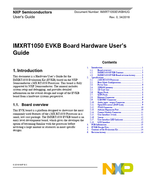
NXP IMXRT1050 EVKB开发板硬件用户指南说明书
© 2018 NXP B.V.IMXRT1050 EVKB Board Hardware User’sGuide1. IntroductionThis document is a Hardware User’s Guide for theIMXRT1050 Evaluation Kit (EVKB) based on the NXP Semiconductor i.MX RT1050 Processor. This board is fully supported by NXP Semiconductor. The manual includes system setup and debugging, and provides detailedinformation on the overall design and usage of the EVKB board from a hardware systems perspective.1.1. Board overviewThis EVK board is a platform designed to showcase the most commonly used features of the i.MX RT1050 Processor in a small, low cost package. The IMXRT1050 EVKB board is an entry level development board, which gives the developer the option of becoming familiar with the processor before investing a large amount or resources in more specific designs.NXP Semiconductors Document Number: IMXRT1050EVKBHUGUser's GuideRev. 0 , 04/2018Contents1.Introduction ........................................................................ 1 1.1. Board overview ....................................................... 1 1.2. IMXRT1050 EVKB Contents ................................. 3 1.3. IMXRT1050 EVKB Board revision history............ 3 2.Specifications ..................................................................... 3 2.1. i.MX RT1050 Processor ......................................... 5 2.2. Boot Mode Configurations ...................................... 5 2.3. Power Tree .............................................................. 6 2.4. SDRAM memory .................................................... 8 2.5. SD Card Slot ........................................................... 8 2.6. Hyper Flash ............................................................. 8 2.7. QSPI Flash .............................................................. 8 2.8. Ethernet Connector ................................................. 9 2.9. USB PHY Connector .............................................. 9 2.10. Audio input / output Connector ............................... 9 2.11. OpenSDA circuit (DAP-Link) ................................ 9 2.12. JTAG Connector ................................................... 10 2.13. Arduino Expansion Port ........................................ 10 2.14. Camera Module Connector ................................... 11 2.15. User Interface Switch ............................................ 11 2.16. Sensor ................................................................... 12 2.17. User Interface LED Indicator ................................ 12 2.18. LCD Interface ....................................................... 13 3.PCB Information .............................................................. 13 4. EVKB Design Files .......................................................... 13 5. Contents of the Evaluation Kit ......................................... 14 6.Revision history (14)IntroductionFeatures of the IMXRT1050 EVKB board are shown in Table 1Specifications 1.2. IMXRT1050 EVKB ContentsThe IMXRT1050 EVKB contains the following items:•IMXRT1050 EVKB Board•USB Cable (Micro B)1.3. IMXRT1050 EVKB Board revision history•EVKB: Mass Product.NOTEEVKB Boards are based on A1 silicon.2. SpecificationsThis chapter provides detailed information about the electrical design and practical considerations of the EVKB Board, and is organized to discuss each block in the Figure 1 of the EVKB board.Figure 1. Block diagramThe overview of the IMXRT1050 EVKB Board is shown in Figure 1 & Figure 2.SpecificationsFigure 2. Overview of the IMXRT1050 EVKB Board (Front side)Figure 3. Overview of the IMXRT1050 EVKB Board (Back side)Specifications 2.1. i.MX RT1050 ProcessorThe i.MX RT1050 is a new processor family featuring NXP's advanced implementation of the ARM Cortex-M7 Core. It provides high CPU performance and best real-time response. The i.MX RT1050 provides various memory interfaces, including SDRAM, Raw NAND FLASH, NOR FLASH,SD/eMMC, Quad SPI, HyperBus and a wide range of other interfaces for connecting peripherals, such as WLAN, Bluetooth™, GPS, displays, and camera sensors. Same as other i.MX processors, i.MXRT1050 also has rich audio and video features, including LCD display, basic 2D graphics, camera interface, SPDIF and I2S audio interface.The i.MX RT1050 applications processor can be used in areas such as industrial HMI, IoT, motor control and home appliances. The architecture's flexibility enables it to be used in a wide variety of other general embedded applications too. The i.MX processor provides all interfaces necessary to connect peripherals such as WLAN, Blueto oth™, GPS, camera sensors, and multiple displays.The more detail information about i.MX RT1050 can be found in the Datasheet and Reference manual.2.2. Boot Mode ConfigurationsThe device has four boot modes (one is reserved for NXP use). The boot mode is selected based on the binary value stored in the internal BOOT_MODE register. Switch (SW7-3 & SW7-4) is used to select the boot mode on the IMXRT1050 EVKB Board.Typically, the internal boot is selected for normal boot, which is configured by external BOOT_CFG GPIOs. The following Table 3 shows the typical Boot Mode and Boot Device settings.NOTEFor more information about boot mode configuration, see the System Boot chapter of theMIMXRT1050 Reference Manual.SpecificationsFor more information about IMXRT1050 EVKB boot device selection and configuration, see the main board schematic.2.3. Power TreeA DC 5V external power supply is used to supply the IMXRT1050 EVKB Board at J2, and a slide switch SW1 is used to turn the Power ON/OFF. J28 and J9 also can be used to supply the EVKB Board. Different power supply need to configure different Jumper setting of J1. Table 4 shows the details:NOTEFor some computers’ USB, it cannot support 500 ma before establishingcommunication. In this case, it is recommended to replace the computer oruse the power adapter(J2) to power the EVKB Board.The power tree is shown in the following figure.Figure 4. Power TreeSpecificationsThe power control logic of the IMXRT1050 EVKB board is shown in Figure 5:•It will power up SNVS firstly, then PMIC_REQ_ON will be switched on to enable external DC/DC to power up other power domains.•ON/OFF button is used to switch ON/OFF PMIC_REQ_ON to control power modes.•RESET button and WDOG output are used to reset the system power.Figure 5. Power Control DiagramThe power rails on the board are shown in Table 5.Specifications1 For silicon A0, DCDC_IN voltage domain is 2.9V~3.1V2.4. SDRAM memoryOne 256 Mb, 166 MHz SDRAM (MT48LC16M16A2B4-6AIT: G) is used on the EVK Board.2.5. SD Card SlotThere is a SD card slot(J20) on the IMXRT1050 EVKB Board.J20 is the Micro SD slot for USDHC1 interface. If the developer wants to boot from the SD Card, the boot device switch (SW7) settings should be: ON, OFF, ON, OFF, as shown in Table 3.2.6. Hyper FlashOn the IMXRT1050 EVKB Board, there is one 512 Mbit Hyper Flash device. If the developer wants to boot from the Hyper Flash, the boot device switch (SW7) settings should be: OFF. ON, ON, OFF, as shown in Table 3.2.7. QSPI FlashA 64Mbit QSPI Flash is used on the IMXRT1050 EVKB Board. If the developer wants to boot from the QSPI Flash, the boot device switch(SW7) settings should be: OFF, OFF, ON, OFF, as shown in Table 3. By default, this QSPI Flash is disabled on the EVKB. To enable the onboard QSPI Flash, the settings need to be changed.Specifications Step1:Removed resistors: R356, R361 - R366.Step2:Weld 0Ωresistors: R153 - R158.2.8. Ethernet ConnectorThere is one Ethernet Mac controller in the MIMXRT1050 processor. The Ethernet subsystem of the IMXRT1050 EVKB Board is provided by the KSZ8081RNB 10/100M Ethernet Transceiver (U16) anda RJ45 (J19) with integrated Magnetic.2.9. USB PHY ConnectorThe MIMXRT1050 contains 2 integrated USB 2.0 PHYs capable of connecting to USB host/device systems at the USB low-speed (LS) rate of 1.5 Mbits/s, full-speed (FS) rate of 12 Mbits/s or at the USB 2.0 high-speed (HS) rate of 480 Mbits/s.2.10. Audio input / output ConnectorThe Audio CODEC used on the IMXRT1050 EVKB Board is Wolfson’s Low Power, high quality Stereo Codec, WM8960.The IMXRT1050 EVKB Board include one headphone interface (J12), one onboard MIC (P1), two speaker interfaces (J16, J17), and the SPDIF interface (J14 & J18, DNP). J12 isa 3.5mm audio stereo headphone jack, which supports jack detect.2.11. OpenSDA circuit (DAP-Link)The OpenSDA circuit (CMSIS–DAP) is an open-standard serial and debug adapter. It bridges serial and debug communications between a USB host and an embedded target processor.CMSIS-DAP features a mass storage device (MSD) bootloader, which provides a quick and easy mechanism for loading different CMSIS-DAP Applications such as flash programmers, run-control debug interfaces, serial-to-USB converters, and more. Two or more CMSIS-DAP applications can run simultaneously. For example, run-control debug application and serial-to-USB converter runs in parallel to provide a virtual COM communication interface while allowing code debugging via CMSIS-DAP with just single USB connection.For the IMXRT1050 EVKB Board, J28 is the connector between the USB host and the target processor. Jumper to serial downloader mode to use stable DAP-Link debugger function. If developer wants to make OpenSDA going to the bootloader mode, J27 should jumper to 1-2, and press SW4 when power on. Meanwhile, the OpenSDA supports drag/drop feature for U-Disk. First, use the seral downloader mode and drag/drop the image file to U-Disk. Then select Hyper Flash as boot device and reset the Board, the image will run.Specifications2.12. JTAG ConnectorJ21 is a standard 20-pin/2.54 mm Box Header Connector for JTAG. The pin definitions are shown in the Figure 6. Support SWD by default.Figure 6. JTAG pin definitions2.13. Arduino Expansion PortJ22 – J25 is defined as Arduino Interface. The pin definitions of Arduino Interface are shown in Table 6.SpecificationsNOTEJ24 PIN9&PIN10 are not compatible with ARDUINO I2C, please use orwire to J23 PIN5&PIN6 instead and it will correct in next revision.2.14. Camera Module ConnectorOne parallel CSI (Camera Sensor Interface) is supported by the i.MX RT1050. There is a Camera Module Connector (J35) on the IMXRT1050 EVKB Board. The CA031C based on OV7725 andCA111C based on MT9M114 can be used directly.NOTEJ35 supports both MT9M114 and OV7725 camera module, but 3.3V is aviolation to MT9M114 spec 3.1V. It proved fine for evaluation/demo with3.3V supply, but in product design, it is recommended to adjust DCDCoutput or add level shifter.2.15. User Interface SwitchThere are four user interface switches on the IMXRT1050 EVKB Board. Their functionality is as below.Specifications2.15.1. Power SwitchSW1 is a slide switch to control the power of the IMXRT1050 EVKB Board when the power supply is from J2. The function of this switch is listed below:•Sliding the switch to the ON position connects the 5 V power supply to the Evaluation board main power system.•Sliding the switch to OFF position immediately removes all power from the board.2.15.2. ON/OFF ButtonSW2 is the ON/OFF button for IMXRT1050 EVKB Board. A short pressing in OFF mode causes the internal power management state machine to change state to ON. In ON mode, a short pressing generates an interrupt (intended to be a software-controllable(power-down). An approximate 5 seconds or more pressing causes a forced OFF. Both boot mode inputs can be disconnected.2.15.3. Reset ButtonThere are two Reset Button on the EVK Board. SW3 is the Power On Reset Button. Pressing the SW3 in the Power On state will force to reset the system power except SNVS domain. The Processor will be immediately turn off and reinitiate a boot cycle from the Processor Power Off state. SW4 is Reset Button.2.15.4. USER ButtonSW8 is the USER Button(GPIO5-00) for developers using. Pressing can produce changes in high and low levels.2.16. SensorU32 on the EVK Board is a 6-Axis Ecompass (3-Axis Mag, 3-Axis Accel) sensor FXOS8700CQ. The Ecompass is connected to i.MX RT1050 I2C1 port.2.17. User Interface LED IndicatorThere are four LED status indicators located on the EVK Board. The functions of these LEDs include: •Main Power Supply(D3)Green: DC 5V main supply is normal.Red: J2 input voltage is over 5.6V.Off: the board is not powered.•Reset RED LED(D15)•OpenSDA LED(D16)•USER LED(D18)EVKB Design Files 2.18. LCD InterfaceThe enhanced Liquid Crystal Display Interface (eLCDIF) is a general purpose display controller.The eLCDIF block supports the following:•Displays that support moving pictures and require the RGB interface mode (DOTCLK interface). The eLCDIF provides fully programmable functionality to supported interfaces:•Bus master interface to source frame buffer data for display refresh.•8/16/18/24/32 bit LCD data bus support available depending on I/O mux options.•Programmable timing and parameters for DOTCLK LCD interfaces.If developers want to use LCD, NXP provides an optional LCD module RK043FN02H-CT which has a 4.3 inches touch-screen and supports a resolution of up to 480*3(RGB)*272. This module contains two FPC cables. The LCD interface can be connected to J8(A1-A40) and the CPT interface can be connected to J8(B1-B6). LCD modules can be purchased from the NXP website.3. PCB InformationThe IMXRT1050 EVKB Board is made using standard 4-layer technology. The material used was FR-4. The PCB stack-up information is shown in Table 7.4. EVKB Design FilesThe schematics, layout files, and gerber files (including Silkscreen) can be downloaded from/MIMXRT1050-EVKRevision history5. Contents of the Evaluation KitNOTEPower adaptor, Micro SD Card, LCD Module and Camera Module are not standard parts of the Evaluation Kit.6. Revision historyTable 9 summarizes the changes made to this document since the initial release.Document Number: IMXRT1050EVKBHUGRev. 0 04/2018How to Reach Us: Home Page: Web Support: /supportInformation in this document is provided solely to enable system and softwareimplementers to use NXP products. There are no express or implied copyright licenses granted hereunder to design or fabricate any integrated circuits based on the information in this document. NXP reserves the right to make changes without further notice to any products herein.NXP makes no warranty, representation, or guarantee regarding the suitability of its products for any particular purpose, nor does NXP assume any liability arising out of the application or use of any product or circuit, and specifically disclaims any and all liability, including without limitation consequenti al or incidental damages. “Typical” parameters that may be provided in NXP data sheets and/or specifications can and do vary in different applications, and actual performance may vary over time. All operating parameters, including “typicals,” must be valid ated for each customer application by customer’s technical experts. NXP does not convey any license under its patent rights nor the rights of others. NXP sells products pursuant to standard terms and conditions of sale, which can be found at the following address: /SalesTermsandConditions . NXP, the NXP logo, NXP SECURE CONNECTIONS FOR A SMARTER WORLD, Freescale, the Freescale logo are the trademarks of NXP B.V. All other product or service names are the property of their respective owners.Arm, the Arm logo, and Cortex are registered trademarks of Arm Limited (or its subsidiaries) in the EU and/or elsewhere.. All rights reserved. © 2018 NXP B.V.。
NXP_产品手册
主要应用:
● 2.5G和3G无线收发器; ● 固定网络; ● 无线基础设施; ● 线缆调制解调器; ● CMTS/DOCSIS; ● GPS导航;
NXP的10bit数据转换器家族中的ADC1006S系列是可满足今天消费 类和专业级高端市场需求的高性能转换器。它只是NXP众多可应用于无 线、医疗、工业等领域的高性能、高速数据转换器中一个系列。
NXP的ADC1006S系列ADC在噪声、信噪比、总谐波失真和有效位数 等方面提供了卓越的性能,此系列器件可以将模拟信号转换为最高以 70MSPS采样的10位二进制数字信号,且对通信和专业级成像应用做了优 化。所有静态数字输入(如:SH、CE和OTC)与TTL/CMOS电平兼容, 所有输出与CMOS电平兼容。时钟输入使用正弦信号亦可。
DAC1401D125是一高速、高性能的双通道 14位DAC,适用 于要求更小的PCB体积和更低的电源消耗场合。
DAC1401D125的两个DAC可以工作于各自的数据输入线, 也可以使用交错模式,通过一个处理器交错地向两个DAC写入数 据,可以通过调节DAC的满量程输出电流以降低电源的消耗,并 可在空闲周期进入睡眠模半导体公司的高速数模转换器(DAC)产品线目前已经拥有125M/160M/650MSPS速度 等级的产品,每个速度等级都有10/12/14bit三个精度等级。可满足无线通信、线缆调制解调器、 医疗/测量仪器等高速系统的应用要求。
全系列的器件均为双通道结构,并为同相/正交传输优化设计,特别适用于通信场合。系列器 件具有卓越的性能/功耗比,当工作在最高速度下依然有出色的动态范围,同时保持很低的功耗。 器件可兼容1.8V/3.3V/5V输入电平,并有很宽的时钟周期范围,可方便与各种处理器连接。其中 160MSPS和650MSPS系列产品带插值滤波功能,可去除频谱中的镜像频率,使输出信号更加平 滑,降低了模拟滤波器的设计要求,使量化噪声分布在更宽的带宽以提高信噪比,内部集成低噪 声免滤波电容锁相环(用于插值滤波器)。
NXP_MOSFET选型手册
Package name TO-236AB TO-236AB SOT883 TSSOP6 SC-75 SOT666 SC-70 TO-236AB TO-236AB TO-236AB TO-236AB TO-236AB TSSOP6 SC-75 SOT666 SC-70 TO-236AB TO-236AB TO-236AB TO-236AB TO-236AB SC-70 TO-236AB TO-236AB TO-236AB TO-236AB TSOP6 TO-236AB SC-73 SC-73 SC-73 SC-73 SC-73 SC-73 SC-73 SC-73 SC-73 SC-73 SC-73 TO-236AB TO-236AB TSSOP6 SC-70 TO-236AB TSSOP6 SC-70 SOT89 TO-236AB TO-236AB SOT883 TSSOP6
RDSon [max] @ VGS = 10 V (mOhm) 5000 1600 1600 1600 1600 1600 1600 1600 3000 2000 3900 1600 1600 1600 1600 1600
RDSon [max] @ VGS = 5 V (mOhm) 2000 2000 2000 2000 2000 2000
-50 -50 -50 200 100 -50 -20 -30 -30 30 30 30 30 30 -30 -30 -30 -30 -30 60 60 60 100 20 25 20 40 55 75 100 55 55 200 55 100 75 60 200 100 150 100 25 30 300 30 55 20 30 25 200 -16 30 100 30
2000 2000 2000 2000 2000
NXP官方LPC系列ARM选型表
22
LPC2141 60 32 8 45 D 1 12
22
LPC2142 60 64 16 45 D 1 12
22
LPC2144 60 128 16 45 D 1 12
22
LPC2146 60 256 40 45 D 1 12
22
LPC2148 60 512 40 45 D 1 12
22
11 8
4 14 Y 3.3
Cortex-M4系列
型号
fmax FLASH RAM
USB
I/Opins USB
USB 速率
定
I/O 电 CPU
CAN UART I²C I²S SPI SSP ADC DAC 时 PWM PLL
(MHz) (kB) (kB)
ports (Mbps)
压 器
(V)
LPC4337 204 1024 136 83
NXP ARM 选型列表
Cortex-M0 LPC1100系列
型号
fmax (MHz)
FLASH (kB)
RAM (kB)
I/Opins
USB
USB ports
USB 速率 (Mbps)
CAN
UART
I²C
I²S
SPI
SSP
ADC
DAC
定 时 器
PWM
PLL
I/O 电 压
CPU
(V)
LPC1113 50 24 4-8 28-42
1
3 6 Y 3.3
2
4
3 6 Y 3.3
2
4
3 6 Y 3.3
2
4
3 6 Y 3.3
2
4
NXP 74系列逻辑门选型指南
NXP advances state-of-the-art packaging with MicroPak (XSON). Designedfor use in portable applications, where board space is always an issue, XSON packages are dramatically smaller, allowing compact and slimmer overall designs. These leadless Mini Logic packages provide up to 65% space saving over traditional leaded Mini Logic (PicoGate) packages.KEY FEATURES• V ery small footprint• 0.5 mm, 0.35 mm, and 0.3 mm pitch options • L ow profile height (0.5 mm or 0.35 mm)• P b-free, RoHS, and dark green compliant • F ully specified (-40 to +125 °C)• A utomotive optionsBENEFITS• S implified board layout• N o bent leads• N o co-planarity issues• L ow power consumption APPLICATIONS• S pace constrained applications• C onsumer• P ortable• A utomotive The MicroPak packages are leadless Mini Logic packages. They house the same silicon die as the larger leaded Mini Logic (PicoGate) packages. This ensures that along with the smaller footprint identical electrical performance is assured. Signal integrity may be improved due to lower package parasitic inductance. Their tiny size saves valuable board real estate. Packages are available with 0.5 mm as well as state of the art 0.35 mm and 0.30 mm pad pitch.The package is an ideal choice for space constrained applications where PCB space and low cost assembly is critical. With their larger pads the MicroPak packages offer easier component placement as well as improved strength, reliability, and thermal characteristics over similar sized BGA solutions.MICROPAK PORTFOLIOThe MicroPak portfolio is very broad and includes analog switches, buffers/inverters/drivers, bus switches, counters, decoders, flip-flops, gates, multiplexers/demultiplexers, latches, level shifters, and Schmitt-trigger devices.MICROPAK PACKAGESThe MicroPak packages include 5-pin XSON and X2SON, 6-pin XSON and X2SON, 8-pin XSON and XQFN variants, as well as 10-pin XSON and XQFN variants.For more information about our MicroPak portfolio visit/products/discretes-and-logic/logic/micropak:GRP_12584For information about automotive compliant devices visit/products/automotive-products/discrete-and-logic/logic:MC_71523© 2016 NXP Semiconductors, B.V.All rights reserved. Reproduction in whole or in part is prohibited without the prior written consent of the copyright owner. The informa-tion presented in this document does not form part of any quotation or contract, is believed to be accurate and reliable and may be changed without notice. No liability will be accepted by the publisher for any consequence of its use. Publication thereof does not convey nor imply any license under patent or other industrial or intellectual property rights.Date of release: April 2016 Published in the USA。
- 1、下载文档前请自行甄别文档内容的完整性,平台不提供额外的编辑、内容补充、找答案等附加服务。
- 2、"仅部分预览"的文档,不可在线预览部分如存在完整性等问题,可反馈申请退款(可完整预览的文档不适用该条件!)。
- 3、如文档侵犯您的权益,请联系客服反馈,我们会尽快为您处理(人工客服工作时间:9:00-18:30)。
The ARM selection guide
NXP is changing the embedded landscape. Our continuum of ARM solutions covers a complete spectrum of designs, from low-cost and low-power to high-performance applications. Our industry-leading microcontrollers include the latest 32-bit LPC4000, LPC3000, LPC2000, and LPC1000 product families. Plus, we offer an easy migration path within our microcontroller families that are pin- and software-compatible. When designers choose NXP, they get more than just one solution; they get a whole range of options for supporting their entire product line, now and in future. LPC1000 family
1024 KB 512 KB
136 KB 136 KB 200 KB
5 5 5 5 5 5 5 5 5 5 5 5 5 5
6 6 6 6 6 6 6 6 6 6 6 6 6 6
1 1 1 1 1 1
2 2 2 2 2 2 1 1 1 1 1
4 4 4 4 4 4 4 4 4 4 4 4 4 4
2 2 2 2 2 2 2 2 2 2 2 2 2 2
CPU voltage
Type
LPC1812 LPC1810
Temp. range options
EEPROM
Ethernet
FLASH
UART
RAM
USB
I2C
I/O voltage
SD/MMC
I/O pins
SSP/SPI
CAN
LCD
PLL
SPI
I2S
Package
LQFP144, TBGA100 LQFP144, TBGA100
1024 KB 512 KB
136 KB 136 KB 200 KB
1024 KB 768 KB 512 KB 512 KB
136 KB 136 KB 104 KB 104 KB 168 KB
1024 KB 768 KB 512 KB
136 KB 136 KB 104 KB
Continued next page
EEPROM
Ethernet
FLASH
UART
RAM
USB
I2C
I/O voltage
SD/MMC
I/O pins
SSP/SPI
CAN
LCD
PLL
SPI
I2S
Package
Comments / special features
Dual Bank Flash, LCD 1024 H x 768 V, HS USB with On-Chip HS PHY, SPI Flash Interface, State Config. Timer. Available Q3 2011 Dual Bank Flash, LCD 102 H x 768 V, HS USB with On-Chip HS PHY, SPI Flash Interface, State Config. Timer. Available Q3 2011 LCD 1024 H x 768 V, HS USB with On-Chip HS PHY, SPI Flash Interface, State Config. Timer. Available Q1 2011 Dual Bank Flash, Hi-Speed USB with On-Chip HS PHY, SPI Flash Interface, State Config. Timer. Available Q3 2011 Dual Bank Flash, Hi-Speed USB with On-Chip HS PHY, SPI Flash Interface, State Config. Timer. Available Q3 2011 Hi-Speed USB with On-Chip HS PHY, SPI Flash Interface, State Config. Timer. Available Q1 2011 Dual Bank Flash, Hi-Speed USB with On-Chip HS PHY, SPI Flash Interface, State Config. Timer. Available Q3 2011 Dual Bank Flash, Hi-Speed USB with On-Chip HS PHY, SPI Flash Interface, State Config. Timer. Available Q3 2011 Dual Bank Flash, Hi-Speed USB with On-Chip HS PHY, SPI Flash Interface, State Config. Timer. Available Q3 2011 Hi-Speed USB with On-Chip HS PHY, SPI Flash Interface, State Config. Timer. Available Q3 2011 Hi-Speed USB with On-Chip HS PHY, SPI Flash Interface, State Config. Timer. Available Q1 2011 Dual Bank Flash, SPI Flash Interface, State Config. Timer. Available Q3 2011 Dual Bank Flash, SPI Flash Interface, State Config. Timer. Available Q3 2011 Dual Bank Flash, SPI Flash Interface, State Config. Timer. Available Q3 2011
The LPC1100 series, based on the ARM Cortex-M0 core, is the lowest-priced 32-bit MCU solution in the market. It delivers unprecedented performance, simplicity, low-power, and dramatic reductions in code size for every application. The LPC1200 series, also based on the Cortex-M0 core, is designed for industrial applications with ADC, comparators, RTC, Windowed WDT, and up to 128 KB of Flash. The LPC1800 and LPC1700 series, based on the ARM Cortex-M3 core and operating at up to 150 MHz, are low-power 32-bit microcontrollers featuring a broad range of serial interfaces and are ideal for a broad range of applications, such as eMetering, medical, POS, and industrial networking. The LPC1300 series, also based on the Cortex-M3 core, are very low-power and include on-chip USB drivers in ROM to greatly simplify USB implementation.
Max. freq. (MHz) Memory Timers PWM channels No. of timers* Serial interfaces Analog ADC channels/ resolution External bus interface DAC (10-bit) channels
• • • • • • • • • • • • • •
150 150 150 150 150 150 150 150 150 150 150 150 150 150
2.0 - 3.6 V 2.0 - 3.6 V 2.0 - 3.6 V 2.0 - 3.6 V 2.0 - 3.6 V 2.0 - 3.6 V 2.0 - 3.6 V 2.0 - 3.6 V 2.0 - 3.6 V 2.0 - 3.6 V 2.0 - 3.6 V 2.0 - 3.6 V 2.0 - 3.6 V 2.0 - 3.6 V
NXP_04_0091_Update_MCU_linecard_939775017103_v3.indd 1
22/04/11 12:57
Max. freq. (MHz)
Memory
Timers PWM channels No. of timers*
Serial interfaces
Analog ADC channels/ resolution External bus interface DAC (10-bit) channels