原子力显微镜的新测试方法——HybriD-Mode
SPA-400 原子力显微镜 操作说明
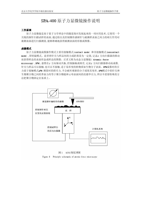
SPA-400原子力显微镜操作说明工作原理原子力显微镜是基于量子力学理论中的隧道效应发展起来的一项应用技术。
它使用一个尖锐的探针扫描试样的表面,通过检出及控制微传感探针与被测样表面之间力的相互作用对被测表面进行扫描测量,能够准确地获得被测表面的形貌或图像。
成像模式原子力显微镜成像操作模式主要有接触模式(contact mode) 和非接触模式(noncontact mode) ,即轻敲模式。
前者将针尖与样品间的力或距离设为一定值,记录z 方向扫描器的移动而获得样品的表面形态或样品的图像; 后者又称为动态力显微镜( dynamic force microscopy ,DFM),悬臂在z 方向驱动共振,控制振幅或相差,记录z 方向扫描器移动而成像,针尖与样品可以接触,也可以不接触,适于易形变的软物质如生物分子表面。
DFM成像时的引力弱于接触模式AFM 测量时的排斥力,不会破坏观察的分子或使其变形。
DFM模式中的针尖和生物聚合物之间的界面力约等于聚合物链和云母表面间的范德华引力,所以不需要特殊的方法把聚合物固定在基质上。
样品的要求原子力显微镜研究对象可以是有机固体、聚合物以及生物大分子等,样品的载体选择范围很大,包括云母片、玻璃片、石墨、抛光硅片、二氧化硅和某些生物膜等,其中最常用的是新剥离的云母片,主要原因是其非常平整且容易处理。
而抛光硅片最好要用浓硫酸与30%双氧水的7∶3 混合液在90 ℃下煮1h 。
利用电性能测试时需要导电性能良好的载体,如石墨或镀有金属的基片。
试样的厚度,包括试样台的厚度,最大为10 mm。
如果试样过重,有时会影响Scanner 的动作,请不要放过重的试样。
试样的大小以不大于试样台的大小(直径20 mm)为大致的标准。
稍微大一点也没问题。
但是,最大值约为40 mm。
如果未固定好就进行测量可能产生移位。
请固定好后再测定。
一、系统的启动将SPI 3800 N电气部分的正面板中央的电源开关打到ON的位置(处于ON的位置时,开关点亮)。
电化学原子力显微镜

AFM应用领域
AFM可以在大气、真空、低温和高温、不同气氛以及溶液等各种环境下工作,且 不受样品导电性质的限制,因此已获得比STM更为广泛的应用。主要用途:
1
• 导体、半导体和绝缘体表面的高分辨成像
2
• 生物样品、有机膜的高分辨成像
3
• 表面化学反应研究
29
AFM可以在大气、真空、低温和高温、不同气氛以及溶液等各种环境下工作,且 不受样品导电性质的限制,因此已获得比STM更为广泛的应用。主要用途:
44
NANO LETTERS 2002 Vol.2,No.10 1055-1060
45
NANO LETTERS 2002 Vol.2,No.10 1055-1060 46
应用举例-AFM对电极表面的修饰
Ag ( 111)在 0. 1 mol / L( KCl)溶液中正常的电
化学氧化发生在45 mV 以上,而还原过程在100 mV前基本完成. 但在ECSTM 针尖的诱导下 Ag 电极可以在较正的0 V 下发生氧化. 在0 V 时,可以观察到电极表面形成一些形状不规则的 AgCl 沉淀物, 且随时间而增多. 几秒钟后当电位 回复至- 400 mV 并扩大扫描范围, 可观察到由 于Ag 的溶解造成的缺陷, 有趣的是这种由针尖 参与的温和的氧化过程仅造成原子层深度的弧 形缺陷,而电极表面在整体上仍然保持单晶面.
要在高真空的环境下操作
6
扫描探针显微镜SPM
SPM是指在STM基础上发展起来的一大类显微镜, 通过探测极小探针与表面之间的物理作用量如光、电、 磁、力等的大小而获得表面信息。
scanning tunneling Microscopy (STM, 1982)
Atomic force microscopy (AFM)
钢中纳米级第二相定量测试-原子力显微镜法

钢中纳米级第二相定量测试-原子力显微镜法下载温馨提示:该文档是我店铺精心编制而成,希望大家下载以后,能够帮助大家解决实际的问题。
文档下载后可定制随意修改,请根据实际需要进行相应的调整和使用,谢谢!并且,本店铺为大家提供各种各样类型的实用资料,如教育随笔、日记赏析、句子摘抄、古诗大全、经典美文、话题作文、工作总结、词语解析、文案摘录、其他资料等等,如想了解不同资料格式和写法,敬请关注!Download tips: This document is carefully compiled by the editor. I hope that after you download them, they can help you solve practical problems. The document can be customized and modified after downloading, please adjust and use it according to actual needs, thank you!In addition, our shop provides you with various types of practical materials, such as educational essays, diary appreciation, sentence excerpts, ancient poems, classic articles, topic composition, work summary, word parsing, copy excerpts, other materials and so on, want to know different data formats and writing methods, please pay attention!钢中纳米级第二相定量测试-原子力显微镜法,是一种非常重要的分析技术,可以帮助我们研究材料的微观结构和性质。
原子力显微镜原理及操作流程讲义bgme

由于光杠杆作用原理,即使小于0.01nm的微悬臂形变 也可在光电检测器上产生10nm左右的激光点位移,由此产 生的电压变化对应着微悬臂的形变量,通过一定的函数变 换便可得到悬臂形变量的测量值。当样品在XY平面内扫描 时(对某一点其坐标为[x,y])若保持样品在Z轴方向静止,且 令探针的竖直初始位置为零,则可根据针尖-样品相互作用 与间距的关系得到样品表面的高度变化信息Δh(x,y),即样 品表面任意点(x,y)相对于初始位点的高度。对样品表面进 行定域扫描便可得到此区域的表面形貌A=A(x,y, Δh(x,y))。
5.3 轻敲模式(Tapping Mode)
• 轻敲模式是上述两种模式之间的扫描方式。扫描时,在 共振频率附近以更大的振幅(>20nm)驱动微悬臂,使得针尖 与样品间断地接触。当针尖没有接触到表面时,微悬臂以一 定的大振幅振动,当针尖接近表面直至轻轻接触表面时,振 幅将减小;而当针尖反向远离时, 振幅又恢复到原值。作用 在样品上的力保持恒定。由于针尖同样品接触,分辨率几乎 与接触模式一样好;又因为接触非常短暂,剪切力引起的样 品破坏几乎完全消失。轻敲模式适合于分析柔软、粘性和脆 性的样品,并适合在液体中成像 。
5.2 非接触模(Non-contact Mode)
非接触模式探测试样表面时悬臂在距离试样表面上方 5~10 nm 的距离处振荡。样品与针尖之间的相互作用由范德
华力控制,通常为 10N12,样品不会被破坏,而且针尖也不
会被污染,适合于研究柔嫩物体的表面。此模式的不利之处 是要在室温大气环境下完成。针尖-样品距离在几到几十纳米 的吸引力区域,对应图3中的3-4段。由于针尖-样品距离较大, 因此分辨率比接触式的低。到目前为止,非接触模式通常不 适合在液体中成像, 在生物样品的研究中也不常见。
原子力显微镜技术参数.doc
原子力显微镜技术参数1测试模式可支持以下模式:ScanAsyt(全自动扫描模式)/Contact AFM(接触模式)/Tapping mode (轻敲模式)/ LiftMode(抬高模式)2详细技术性能要求:2.1噪音:RMS < 0.3 Å (垂直方向),横向分辨率:0.2nm (XY方向),可得到稳定的云母原子像。
*2.2扫描方式:样品扫描,保证最短机械回路,最低噪音控制,需要提供样品扫描方式工作。
探针、探针支架、激光反馈装置保持静止。
扫描管为可软件线性校准管状扫描管。
2.3 LiftMode(抬高模式)测试具备设定:First Lift Height (初始抬高高度),Lift Height( 测试抬高高度),Negative LiftMode( 负抬高模式,实现纳米操纵的精确测试)。
*2.4管状扫描器二个,要求两个扫描管都可以兼容AFM,精确度不低于扫描器XY:8μm×8μm,Z:2.5 μm扫描器XY:120μm×120μm,Z:5 μm2.5可8通道同时采集数据1024 x 1024,3通道同时采集数据5120 x 5120 ,最大数量采样16384 x 1600。
大范围扫描可以同时得到更多细节并且测试多种数据分析。
同时可提供10X快速扫描功能。
*2.6具有负抬高功能(Negative LiftMode),以达成纳米操纵(如DNA操纵)的实验要求。
可通过Digital Q Control功能,提高信噪比,可提高10X或降低10X。
*2.7 Tapping mode (轻敲模式)模式具备两种测试功能:Tapping-TR反馈轻敲模式(Z 方向振幅)信号,同时监测Torsional amplitude。
TR Mode 反馈直接是信号Torsional amplitude。
TR模式可以通过检测横向的振幅信号,更好的追踪表面形貌,实现对粘性很强的样品测试及各向异性材料的不同方向特性检测。
原子力学显微镜的工作模式

缺点
轻敲模式( tapping mode)
• 当针尖没有接触到表面时, 微悬臂以一定的大振幅振动, 当针尖接近表面直至轻轻接 触表面时,其振幅将减小。
•反馈系统通过调整样品与针 尖间距来控制微悬臂振幅与 相位,使得作用在样品上的 力保持恒定,记录样品的上 下移动情况即在Z方向上扫 描器的移动情况来获得图像。
非接触模式的优缺点
• 没有力作用于样品表面。
优点
• 由于针尖与样品分离,横向分辨率低;为了避免接触吸 附层而导致针尖胶粘,其扫描速度低于Tapping Mode和 Contact Mode AFM。通常仅用于非常怕水的样品,吸附 液层必须薄,如果太厚,针尖会陷入液层,引起反馈不 稳,刮擦样品。由于上述缺点,non-contact Mode的使 用受到限制。
原子力显微镜的工作模式
航空宇航制造工程704系
ZY1007152 杜平梅
AFM的工作模式
原子力显微镜(AFM)的工作模式是以针尖与样品之 间的作用力的形式来分类的,主要有以下3种操作模式:
接触模式(contact mode) 非接触模式( non - contact mode)
轻敲模式( tapping mode)
接触模式(contact mode)
接触模式是AFM最直接的成像模式
探针针尖始终与样品表面保持亲密的接触,相互作 用力是排斥力,也称排斥力模式。 扫描时,悬臂施加在针尖上的力有可能破坏试样的 表面结构,因此力的大小范围在10^-10 ~10 ^-6N
接触模式分为恒高模式(constant-height mode)和恒力 模式(constant-force mode)
•微悬臂的高频振动,使 得针尖与样品之间频繁 接触的时间相当短,针 尖与样品可以接触,也 可以不接触。 •有足够的振幅来克服样 品与针尖之间的粘附力。 因此对样品的损害很小, 适用于柔软、易脆和粘 附性较强的样品,且不 对它们产生破坏。
原子力显微镜(AFM)—上海交大分析测试中心
3.2 磁力(MFM)显微镜
1982年
扫描隧道 显微镜
人类第一次能够实时 地观察单个原子在物质表 面的排列状态和与表面电 子行为有关的物理、化学 性质,在表面科学、材料 科学、生命科学等领域的 研究中有着重大的意义和 广阔的应用前景,被国际 科学界公认为八十年代世 界十大科技成就之一。
1.1扫描探针显微镜的产生
扫描隧道显微镜 (STM)
2.2 力-距离曲线
三.扫描力显微镜的分类
3.1 原子力显微镜 3.1.1 斥力模式AFM 3.1.2 摩擦力显微镜 3.1.3 化学力显微镜 3.1.4 检测材料不同组分的技术 a. 相位成像技术 b .力调制技术 3.1.5 检测材料纳米硬度的技术
3.2 磁力显微镜 3.3静电力显微镜
3.1 原子力显微镜ຫໍສະໝຸດ 3.1.1 斥力模式AFM 探针与样品之间进行原子间接触,利用它们
之间的斥力得到样品表面的形貌。 具有两种工作模式:
3.1.1.1 接触模式 3.1.1.2 敲击模式(间歇接触)
3.1.1.1 接触模式(Contact Mode)
接触模式 非接触模式
轻敲模式
接触模式探针
接触模式探针示意图
接触模式工作示意图
Dendrimer-like Gold Nanoparticle[3]
DNA Translocation in Inorganic Nanotubes[4]
现代材料分析方法-原子力显微镜
这种静电排斥随探针与样品表面原子进一步靠近,逐渐抵消原 子间的吸引力.当原子间距离小于1nm,约为化学键长时,范 德华力为0.当合力为正值(排斥)时,原子相互接触.由于在 接触区域范德华力曲线斜率很高,范德华斥力几乎抵消了使探 针进一步靠近样品表面原子的推力.当探针弹性系数很小时, 悬臂发生弯曲.通过检测这种弯曲就可以进行样品形貌观察。 假如设计很大弹性系数的硬探针给样品表面施加很大的作用力, 探针就会使样品表面产生形变或破坏样品表面.这时就可以得 到样品力学信息或对样品表面进行修饰.
单击添加副标题
其他显微 分析方法
202X CIICK HERE TO ADD A TITLE
一、原子力 显微镜原理
AFM的原理较为简单,它是用微小探针 “摸索”样品表面来获得信息.如图3.1所 示,当针尖接近样品时,针尖受到力的作 用使悬臂发生偏转或振幅改变.悬臂的这 种变化经检测系统检测后转变成电信号传 递给反馈系统和成像系统,记录扫描过程 中一系列探针变化就可以获得样品表面信 息图像.下面分别介绍检测系统、扫描系 统和反馈控制系统。
针尖因素
AFM成像实际上是针尖形状与表面形貌 作用的结果,针尖的形状是影响侧向分 辨率的关键因素。针尖影响AFM成像主 要表现在两个方面:针尖的曲率半径和 针尖侧面角,曲率半径决定最高侧向分 辨率,而探针的侧面角决定最高表面比 率特征的探测能力.如图3.4所示,曲率 半径越小,越能分辨精细结构.
图3.1 AFM原理图
检测系统
悬臂的偏转或振幅改变可以通过多种方法检测,包 括:光反射法、光干涉法、隧道电流法、电容检测 法等。目前AFM系统中常用的是激光反射检测系统, 它具有简便灵敏的特点。激光反射检测系统由探针、 激光发生器和光检测器组成。
物理实验技术中的原子力显微镜操作与测量技巧
物理实验技术中的原子力显微镜操作与测量技巧物理实验技术中的原子力显微镜(Atomic Force Microscopy, AFM)作为一种先进的表面形貌和力学性能的测试手段,被广泛应用于各个领域的研究中。
通过AFM,我们可以实时观测微纳米尺度的表面结构和力学性能,并对材料的性质进行分析和评估。
然而,要获得高质量的结果,操作与测量技巧是非常关键的。
一、准备工作在进行原子力显微镜实验之前,我们首先要做好准备工作。
首先,确保实验室环境的洁净度,尽量避免灰尘和污染物对样品的干扰。
其次,对原子力显微镜进行必要的校准和调整,包括扫描探针的选择和安装、扫描头和样品的对齐等。
最后,保持样品的稳定性,避免因温度、湿度等环境因素引起的样品变形和脱落。
二、扫描模式选择在使用原子力显微镜进行观测和测量时,我们需要选择合适的扫描模式。
常见的扫描模式有接触模式、非接触模式和侧向力模式等。
接触模式是最常用的模式,其将探测器固定在采样上方,通过控制探针和样品之间的接触力,实时观测样品表面的形貌。
非接触模式则是在探针和样品之间减小接触力,通过测量探针与样品之间的相互作用力,来获得样品表面的形貌信息。
侧向力模式则是结合接触模式和非接触模式,可以同时观测表面形貌和力学性能。
三、参数设置在进行原子力显微镜实验时,合适的参数设置是非常关键的。
首先,在选择扫描速率时,我们需要根据样品的表面特性、扫描模式和所需分辨率等因素进行综合考虑。
较低的扫描速率可以提高分辨率,但同时也会增加实验时间。
其次,设置合适的探测力是非常重要的。
如果探测力过大,会对样品表面造成损伤;而过小的探测力则可能导致信号噪音过大。
另外,选择合适的扫描范围和数据点密度也需要根据具体需求进行调整。
四、图像处理与数据分析在获得原子力显微镜图像后,我们需要进行图像处理和数据分析才能获得有意义的结果。
常用的图像处理方法包括平滑处理、滤波处理和拟合等。
平滑处理可以去除图像中的噪音点,提高图像质量。
原子力显微镜相位模式
原子力显微镜相位模式
原子力显微镜相位模式是一种高级显微镜技术,它利用原子力显微镜来观察材料的表面形貌和物理性质。
相位模式是原子力显微镜的一种工作模式,它通过测量样品表面的相位差来获得高分辨率的表面形貌图像。
相位模式的工作原理是利用原子力显微镜探针与样品表面之间的相互作用来获取表面形貌信息。
在相位模式下,原子力显微镜的探针会跟随样品表面的起伏变化而上下移动,同时测量探针的位置变化。
通过分析探针的位置变化,可以得到样品表面的相位信息,从而生成高分辨率的表面形貌图像。
原子力显微镜相位模式具有高分辨率、高灵敏度和宽波段的优点。
它可以用于观察纳米尺度的表面形貌和物理性质,对于材料科学、纳米技术和生物医学等领域具有重要的应用价值。
相位模式可以帮助科研人员了解材料的微观结构和性质,为材料设计和制备提供重要参考。
除了表面形貌观察,原子力显微镜相位模式还可以用于研究样品的力学性质、电学性质和磁学性质等。
通过在不同条件下对样品进行相位模式观察,可以获取更加全面的样品信息,为材料研究和应用提供更多的参考数据。
总的来说,原子力显微镜相位模式是一种非常重要的显微镜技术,它在科学研究、材料分析和纳米技术领域发挥着重要作用。
随着原子力显微镜技术的不断发展,相位模式将会更加广泛地应用于材料科学、生物医学和纳米技术等领域,为人类的科学研究和生产生活带来更多的创新和进步。
- 1、下载文档前请自行甄别文档内容的完整性,平台不提供额外的编辑、内容补充、找答案等附加服务。
- 2、"仅部分预览"的文档,不可在线预览部分如存在完整性等问题,可反馈申请退款(可完整预览的文档不适用该条件!)。
- 3、如文档侵犯您的权益,请联系客服反馈,我们会尽快为您处理(人工客服工作时间:9:00-18:30)。
HybriD™Mode Atomic Force Microscopy(AFM) from NT-MDT-An Interview with Sergei Magonov Interview by Will SoutterAZoNano talks to Sergei Magonov about NT-MDT's new HybriD™AFM Mode,which combines the best aspects of contact and oscillatory modes,opening up new applications of AFM technology.WS:NT-MDT has just announced a new AFM mode–HybriD™Mode,or HD-AFM™Mode.Can you give us an overview of how this new mode works,and what it offers?SM:HD-AFM™Mode synergistically combines the best attributes of contact and oscillatory AFM modes.In contact mode,the probe deflection is directly related to the applied force,but lateral forces may induce tip and sample damage. The resonant oscillatory modes(amplitude modulation,tapping mode,intermittent contact,etc.)greatly reduce the lateral tip-sample forces;however,the measured probe amplitude is related to the tip-sample forces in a very complicated way that precludes quantitative nanomechanical measurements.A key advantage of the new HD-AFM™Mode,in which the oscillatory intermittent tip-sample contact happens at frequencies lower than the scanner and probe resonances,is that the probe deflection is directly related to the tip-sample forces.Our proprietary fast acquisition and processing of deflection curves in the HD-AFM™Mode helps extract a whole bank of the force data related to the mechanical(adhesion,stiffness,elastic modulus,etc.)and electromagnetic properties(surface potential,dielectric response,magnetic domains)involved in nanoscale tip-sample interactions.These properties are mapped simultaneously and independently with the imaging of sample topography.Examples of the HD-AFM™Mode applications that demonstrate current capabilities are available as a webinar and application note.HybriD AFM™controller for NT-MDT AFM platformsWS:What are the main benefits of HD-AFM™compared to the range of AFM modes already available to users?SM:The tip-sample forces in HD-AFM™Mode differ from those in other contact and oscillatory modes by magnitude and duration, therefore,the researchers can expect exciting observations of new effects with improvements in the visualization of morphology and nanostructure for complex materials.HD-AFM™Mode opens a pathway towards real-time quantitative studies of local nanomechanical properties on a broader range of materials.Particularly,we believe that this mode can facilitate studies of time-dependent mechanical properties such as viscoelasticity.WS:What are the main application areas that HD-AFM™is designed for?SM:Actually,the practical results obtained with the HD-AFM™Mode have definitely revealed a wider range of applications than other modes can offer.The development of the oscillatory non-resonant mode opens the compositional mapping and quantitative nanomechanical studies of materials with elastic modulus larger than10GPa,which are typically beyond the range of applications using the oscillatory resonant modes.Imaging biological and material samples under liquid also benefits from the use of HD-AFM™Mode as the non-resonant method eliminates the forest of resonant peaks during experimental set-up thus significantly improving the ease of use and speed to results.Hybrid Mode height image(left)and adhesion and stiffness maps,which were obtained in Hybrid mode study of polymerfilm of polystyrene/polybutadiene blend.This very challenging sample was chosen because of the large mismatch inmodulus between the two components and the added complexity of the strong viscoelastic response of Polybutadiene.Although there are currently no adaptive models to accurately calculate both the elastic response of Polystyrene and the viscoelastic response of Polybutadiene when collect in an image map,Hybrid mode does reveal morphology and variations of local properties of this immiscible composition down to tens of nanometers dimensions.WS:How did you come up with the idea to develop this new mode?SM:One of our goals is to continuously improve and provide new capabilities to benefit research in the scientific community,and we believed that could impact key areas of compositional mapping and quantitative nanomechanical properties.From an instrumentation perspective,part of the new HD-AFM™Mode arose from a practical implementation based on the novel technology developments of our electronic controllers,which recently brought substantial benefits to our microscopes by reducing the noise of the probe amplitude detection(down to25fm/sqrtHz)and through fast data acquisition and processing.This technology formed a solid platform for expansion of the AFM functions and the introduction of the HD-AFM™Mode.WS:How will HD-AFM™set NT-MDT’s instruments apart from your competition?SM:Our mission is to provide customers with a comprehensive suite of scanning probe microscopy capabilities to help make their research leading-edge and most efficient.Regarding the HD-AFM™Mode itself,we believe its operation is superior to othernon-resonant oscillatory modes available in the market and we are currently proving that with comparative studies on a challenging set of samples.Moreover,with the addition of HD-AFM™,the NT-MDT microscopes are now equipped with the broadest range of capabilities on the market.Our instruments enable researchers to conduct advanced single-pass electric studies in amplitude modulation mode,which provides simultaneous measurement of topography,surface potential,and dielectric response.We are also working towards quantitative electrical property analysis based on such data.The chemical characterization of materials is achieved by the combination of AFM with confocal Raman scattering in our NT-MDT Spectra microscope.The single-pass electric measurements and HD-AFM™Mode studies are also available in this instrument.Brush macromolecules on mica substrates are visualized in the height images obtained in amplitude modulation andHybrid mode,whereas only in the latter case side chains are clearly resolved.Sample of brush macromolecules–courtesy of Prof.S.Sheiko(UNC).WS:Which AFMs in the NT-MDT range will the new mode be available for?What will the upgrade process be like for users?SM:The HD-AFM™Mode is available on all four of our major instrument platforms;NTEGRA,NEXT,Spectra,and LIFE.The implementation of HD-AFM™Mode is directly related to a novel fast data acquisition module that can be added for recent electroniccontrollers.Contact your local NT-MDT representative for upgrade details specific to your microscope.WS:Are there plans to extend the new capabilities to the other instruments in your product range?SM:Such plans not only exist,they are already being implemented!WS:Can you give us any clues about what other developments to expect from NT-MDT in the near future?SM:Generally speaking,the practical realization of true quantitative nanomechanical and quantitative electrical property measurements at the nanoscale,in broad frequency and temperature ranges,is on our path.Efforts in this direction could be easily coupled to the increasing interest of researchers in chemical characterization by combining AFM with spectroscopic methods.Height images obtained in Hybrid Mode of alkane layers of different chain lengths demonstrate the high-resolutioncapability of this technique enabling the ability to resolve the packing of individual chains(inset image)in the image of C390H782lamellae.Sample of C390H782alkane–courtesy of Prof.G.Ungar(Sheffield University).WS:Where can we find more information about HD-AFM™,and NT-MDT AFM products in general?SM:There are application notes and datasheets available on the NT-MDT website.In addition,a recording of our recent webinar with Virgil Elings and Sergei Magonov,New HD-AFM™Mode;Your Path to Controlling Forces for Precise Material Properties is available to view and download.About Sergei MagonovDr.Sergei Magonov received a doctorate in physics and mathematics from the Moscow Institute of Physics and Technology.Sergei has published over200peer-reviewed papers,1book,and15book chapters.He is now CEO of NT-MDT Development,an R&D subsidiary that was established for the development of novel experimental and applications capabilities using NT-MDT microscopes.Date Added:Jul2,2013|Updated:Jul30,2013NT-MDTNT-MDTPost Box158,Building317-AZelenogradMoscow,124482Russian FederationPH:7(495)5350305Fax:7(495)9135739Email:spm@ntmdt.ruVisit NT-MDT WebsitePrimary ActivityComponent SupplierCompany BackgroundNT-MDT Co.was established in1991with the purpose to apply all accumulated experience and knowledge in the field ofnanotechnology to supply researchers with the instruments suitable to solve any possible task laying in nanometer scale dimensions.The company NT-MDT was founded in Zelenograd-the center of Russian Microelectronics.The products development are based on the combination of the MEMS technology,power of modern software,use of high-end microelectronic components and precision mechanical parts.As a commercial enterprise NT-MDT Co.exists from1993.Now the NT-MDT team develops for you the complete line of SPMs which cover most of scientific and industrial applications.The first NT-MDT device was designed in1990and was called STM-MDT-1-90(Scanning Tunneling Microscope).Till now,this firstmicroscope duly runs in the Institute of Cristallography RAS(Russia).STM-4was developed in1993.The device model Solver appeared in1995starting the Solver product line.The same year the model Solver P47was made.1998was marked by Solver LS, Stand Alone SMENA systems.Special SPM for biological applications called Solver BIO supplemented NT-MDT product line in1999.The next year we developed X,Y Scanning stage for closed-loop operation.Now we can offer you the whole SPM line including AFMs,STMs,SNOMs for almost all possible applications and we continue development of new powerful tools for you..We also supply a wide range of silicon probes and calibration gratings production, design and development that allows us to understand and meet your requirements better.550employees include Ph.D.scientists,many leaders in their field.More than600installations in39countries,more then15year in the SPM market,worldwide distribution of our devices.Our clients are Universities and colleges,laboratories,government and private industrial companies,research centers and small scientific companies on the nanotechnology fieldNT-MDT Co.has two mottos-"Fairness,Intellect,Quality"and"What seems the future to others is the present for us".The bases to successful development are:the best"brains",the best components,high technologies,up-to-date marketing and control.In summary we have:powerful software,best electronics,best mechanics,micro robotics and sales in the world market.Territories ServicedWorldwide。