
74ls574芯片中文使用手册说明书
特点: 逻辑图
说明:
LS574的八个触发器是边沿触发D 型触发器。
在时钟的正跳动,Q 输出将处于D 输入端已建立的逻辑状态。
时钟线上的施密特触发缓冲输入将简化系统设计,因为输入滞后作用使交流和直流抗扰度一般提高400mV 。
缓冲输出的控制输入将使八个输出处于正常状态(高电平或低电平)或处于高阻状态。
在高阻态下,输出既不能有效地给总线加负载,也不能有效地驱动总线。
输出控制不影响触发器的内部工作,既老数据可以保持,甚至当输出被关闭,新的数据也可以置入。
·三态总线驱动输出 ·置数全并行存取 ·缓冲控制输入
·时钟输入有改善抗扰度的滞后作用 外引线排列图
功能表
输入
输出控制 时钟 数据
输出 CLK D Q L ↑ H H L ↑ L L L L × Q O H × × Z H=高电平 L=低电平 ×=不定 Z=高阻态
↑=从低转换到高电平 Q O=建立稳态输入条件前Q 的电平
推荐工作条件
74Ⅱ 54 参数值 参数值 符号 参数名称 最小典型最大最小典型 最大 单位Vcc 电源电压 4.75 5 5.25 4.5 5 5.5 V V IH 输入高电平电压 2.0 2.0 V V IL 输入低电平电压 0.8 0.7 V I OH 输出高电平电流 -2.6 -1 mA I OL 输出低电平电流 24 12 mA 高 15 15 ns t W 时钟脉冲宽度
低
15 15 ns t su 数据建立时间 20↑ 20↑ ns t h 数据保持时间 0↑ 0↑ ns T A
工作环境温度
-40
85
-55
125
℃
电 性 能:(除特别说明外,均为全温度范围)
74Ⅱ
54
参数值
参数值
符号
参数名称
测试条件
最小典型最大最小典型 最大 单位V IK 输入钳位电压
Vcc=最小 I I =-18mA
-1.5 -1.5 V V OH 输出高电平电压
Vcc=最小 V IL =最大
V IH =2V I OH =最大 2.4 2.4 3.4
V V OL 输出低电平电压
Vcc=最小 V IL =最大
V IH =2V I OL =最大
0.5 0.25 0.4
V
I I 输入电流 (最大输入电压时)
Vcc=最大 V I =7V
0.1 0.1 mA I IH 输入高电平电流 Vcc=最大 V I =2.7V 20 20 μA
I IL 输入低电平电流 Vcc=最大 V I =0.4V
-0.4 -0.4 mA I OZH 高关态输出电流
Vcc=最大 V I =2.0V
V o=2.7V
20 20
μA
I OZL 低关态输出电流
Vcc=最大 V I =2.0V
V o=0.4V
-20 -20 μA I OS 输出短路电流 Vcc =最大 V O =0V -30 -130-30 -130 mA I CC 电源电流 Vcc=最大 (注)
40
27
40 mA
注:Icc 在输出控制端加4.5V 时测量。
所有典型值均在Vcc=5.0V , T A =25℃下测量得出。
交流(开关)参数:Vcc=5.0V , T A =25℃
参数值
符号 参数名称 从(输入) 到(输出)测试条件 最小 典型 最大 单位
fmax 最大时钟频率 35 50 MHz t PLH 传输延迟 15 28
t PHL 传输延迟 时钟 CLK 19 28 ns
t PZH 传输延迟 20 28
t PZL 传输延迟 输出控制
C L =45pF R L =667Ω
21 28 ns
t PHZ 传输延迟 12 20
t PLZ
传输延迟
输出控制
任一Q
C L =5pF R L =667Ω
14 25
ns。
KK74ACT574DW中文资料
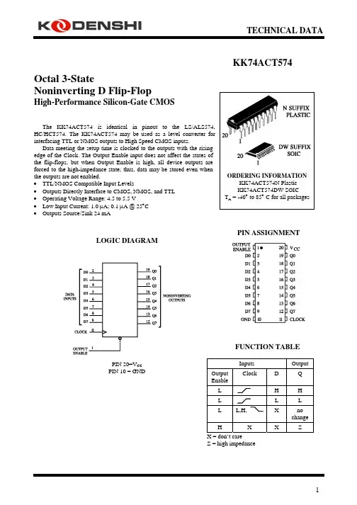
TECHNICAL DATAKK 74ACT574Octal 3-StateNoninverting D Flip-FlopHigh-Performance Silicon-Gate CMOSThe KK HC/HCT574. The KK 74ACT574 may be used as a level converter for interfacing TTL or NMOS outputs to High Speed CMOS inputs.Data meeting the setup time is clocked to the outputs with the rising edge of the Clock. The Output Enable input does not affect the states of the flip-flops, but when Output Enable is high, all device outputs are forced to the high-impedance state; thus, data may be stored even whenthe outputs are not enabled.• TTL/NMOS Compatible Input Levels• Outputs Directly Interface to CMOS, NMOS, and TTL• Operating Voltage Range: 4.5 to 5.5 V• Low Input Current: 1.0 µA; 0.1 µA @ 25°C• Outputs Source/Sink 24 mAFUNCTION TABLEX = don’t careZ = high impedancePIN ASSIGNMENTLOGIC DIAGRAMPIN 20=V CCPIN 10 = GNDMAXIMUM RATINGS*Symbol Parameter ValueUnit V CC DC Supply Voltage (Referenced to GND) -0.5 to +7.0 VV IN DC Input Voltage (Referenced to GND) -0.5 to V CC +0.5 VV OUT DC Output Voltage (Referenced to GND) -0.5 to V CC +0.5 VI IN DC Input Current, per Pin ±20 mAI OUT DC Output Sink/Source Current, per Pin ±50 mAI CC DC Supply Current, V CC and GND Pins ±50 mAP D Power Dissipation in Still Air, Plastic DIP+ SOIC Package+ 750500mWTstg Storage Temperature -65 to +150 °CT L Lead Temperature, 1 mm from Case for 10 Seconds(Plastic DIP or SOIC Package)260 °C*Maximum Ratings are those values beyond which damage to the device may occur.Functional operation should be restricted to the Recommended Operating Conditions.+Derating - Plastic DIP: - 10 mW/°C from 65° to 125°CSOIC Package: : - 7 mW/°C from 65° to 125°CRECOMMENDED OPERATING CONDITIONSSymbol Parameter MinMaxUnit V CC DC Supply Voltage (Referenced to GND) 4.5 5.5 VV IN, V OUT DC Input Voltage, Output Voltage (Referenced to GND) 0 V CC VT J Junction Temperature (PDIP) 140 °CT A Operating Temperature, All Package Types -40 +85 °CI OH Output Current - High -24 mAI OL Output Current - Low 24 mAt r, t f Input Rise and Fall Time *(except Schmitt Inputs) V CC =4.5 VV CC =5.5 V108.0ns/V* VINfrom 0.8 V to 2.0 VThis device contains protection circuitry to guard against damage due to high static voltages or electric fields. However, precautions must be taken to avoid applications of any voltage higher than maximum rated voltages to this high-impedance circuit. For proper operation, V IN and V OUT should be constrained to the range GND≤(V IN or V OUT)≤V CC.Unused inputs must always be tied to an appropriate logic voltage level (e.g., either GND or V CC). Unused outputs must be left open.DC ELECTRICAL CHARACTERISTICS (Voltages Referenced to GND)V CC Guaranteed Limits Symbol Parameter TestConditions V25 °C -40°C to85°CUnitV IH Minimum High-Level Input Voltage V OUT=0.1 V or V CC-0.1 V 4.55.52.02.02.02.0VV IL Maximum Low -Level Input Voltage V OUT=0.1 V or V CC-0.1 V 4.55.50.80.80.80.8VV OH Minimum High-Level Output Voltage I OUT≤ -50 µA 4.55.54.45.44.45.4V*VIN=V IH or V ILI OH=-24 mAI OH=-24 mA4.55.53.864.863.764.76V OL Maximum Low-Level Output Voltage I OUT≤ 50 µA 4.55.50.10.10.10.1V*VIN=V IH or V ILI OL=24 mAI OL=24 mA4.55.50.360.360.440.44I IN Maximum InputLeakage CurrentV IN=V CC or GND 5.5±0.1 ±1.0 µA∆I CCT Additional Max.I CC/InputV IN=V CC - 2.1 V 5.5 1.5 mAI OZ Maximum Three-State LeakageCurrent V IN (OE)= V IH or V ILV IN =V CC or GNDV OUT =V CC or GND5.5±0.5 ±5.0 µAI OLD+Minimum DynamicOutput CurrentV OLD=1.65 V Max 5.575 mAI OHD+Minimum DynamicOutput CurrentV OHD=3.85 V Min 5.5-75 mAI CC Maximum QuiescentSupply Current(per Package)V IN=V CC or GND 5.58.0 80 µA* All outputs loaded; thresholds on input associated with output under test.+Maximum test duration 2.0 ms, one output loaded at a time.AC ELECTRICAL CHARACTERISTICS (V CC=5.0 V ± 10%, C L=50pF, Input t r=t f=3.0 ns)GuaranteedLimits Symbol Parameter 25 °C -40°C to 85°C UnitMin Max MinMaxf max Maximum Clock Frequency (50% Duty Cycle)(Figure 1)100 85 MHz t PLH Propagation Delay, Clock to Q (Figure 1) 2.5 11 2.0 12 nst PHL Propagation Delay, Clock to Q (Figure 1) 2.0 10 1.5 11 nst PZH Propagation Delay, Output Enable to Q (Figure 2) 2.0 9.5 1.5 10 nst PZL Propagation Delay, Output Enable to Q (Figure 2) 2.0 9.0 1.5 10 nst PHZ Propagation Delay, Output Enable to Q (Figure 2) 2.0 10.5 1.5 11.5 nst PLZ Propagation Delay, Output Enable to Q (Figure 2) 2.0 8.5 1.5 9.0 nsC IN Maximum Input Capacitance 4.5 4.5 pFTypical @25°C,V CC=5.0 VC PD Power Dissipation Capacitance 40 pFTIMING REQUIREMENTS (V CC=5.0 V ± 10%, C L=50pF, Input t r=t f=3.0 ns)GuaranteedLimit Symbol Parameter 25°C -40°C to 85°C Unitt SU Minimum Setup Time, Data to Clock (Figure 3) 2.5 2.5nst h Minimum Hold Time, Clock to Data (Figure 3) 1.0 1.0nst w Minimum Pulse Width, Clock (Figure 1) 3.0 4.0 nsFigure 1. Switching Waveforms Figure 2. Switching WaveformsFigure 3. Switching WaveformsEXPANDED LOGIC DIAGRAM。
74hc573完整中文资料
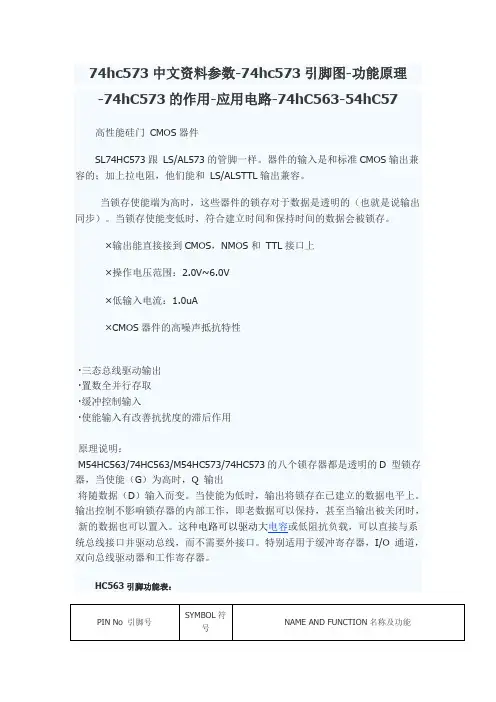
74hc573中文资料参数-74hc573引脚图-功能原理-74hC573的作用-应用电路-74hC563-54hC57高性能硅门CMOS器件SL74HC573跟LS/AL573的管脚一样。
器件的输入是和标准CMOS输出兼容的;加上拉电阻,他们能和LS/ALSTTL输出兼容。
当锁存使能端为高时,这些器件的锁存对于数据是透明的(也就是说输出同步)。
当锁存使能变低时,符合建立时间和保持时间的数据会被锁存。
×输出能直接接到CMOS,NMOS和TTL接口上×操作电压范围:2.0V~6.0V×低输入电流:1.0uA×CMOS器件的高噪声抵抗特性·三态总线驱动输出·置数全并行存取·缓冲控制输入·使能输入有改善抗扰度的滞后作用原理说明:M54HC563/74HC563/M54HC573/74HC573的八个锁存器都是透明的D 型锁存器,当使能(G)为高时,Q 输出将随数据(D)输入而变。
当使能为低时,输出将锁存在已建立的数据电平上。
输出控制不影响锁存器的内部工作,即老数据可以保持,甚至当输出被关闭时,新的数据也可以置入。
这种电路可以驱动大电容或低阻抗负载,可以直接与系统总线接口并驱动总线,而不需要外接口。
特别适用于缓冲寄存器,I/O 通道,双向总线驱动器和工作寄存器。
HC563引脚功能表:HC573引脚功能表:图1 HC573引脚图图2 HC573 国际电工委员会逻辑符号图3 HC563引脚图图4 HC563 国际电工委员会逻辑符号图5 HC563 逻辑图图6 HC573 逻辑图图7 输入输出等效电路真值表:ABSOLUTE MAXIMUM RATINGS绝对最大额定值:Top Operating Temperature: M54HC Series M74HC Series 操作温度:M54HC系列M74HC系列-55 to +125 -40 to +85℃tr,tf Input Rise and Fall Time输入上升和下降时间VCC =2V0 to 1000ns VCC=4.5V0 to 500VCC =6V0 to 400VOHHigh Level Output Voltage输出高电平电压2.0 VI = VIH or VILIO=-20 μA1.92.0-1.9 -1.9 -V4.54.44.54.44.4---6.05.96.05.95.9-4.5IO=-6.0mA4.184.314.134.10-6.0IO=-7.8 mA5.685.85.635.60-VOLLow Level Output Voltage输出低电平电压2.0 VI = VIH or VILIO=20μA-0.0 0.1 -0.1-0.1V4.5-0.00.1 0.10.16.0-0.00.10.10.14.5IO=6.0mA-0.170.260.330.406.0IO=7.8mA-0.180.260.330.40IIInput Leakage Current输入漏电流6.0VI =VCC or GND--±0.1-±1±1μA IOZState Output Off State Current关断状态3态输出电流6.0VI =VIH or VIL VO =VCC or GND--±0.5-±5.0-±10μAICCQuiescent Supply Current静态电源电流6.0VI =VCC or GND--4-40-80μA应用电路图:点击图片查看大图图8。
74系列芯片数据手册大全

74系列芯片数据手册大全74系列芯片数据手册大全74系列集成电路名称与功能常用74系列标准数字电路的中文名称资料7400 TTL四2输入端四与非门7401 TTL 集电极开路2输入端四与非门7402 TTL 2输入端四或非门7403 TTL 集电极开路2输入端四与非门7404 TTL 六反相器7405 TTL 集电极开路六反相器7406 TTL 集电极开路六反相高压驱动器7407 TTL 集电极开路六正相高压缓冲驱动器7408 TTL 2输入端四与门7409 TTL 集电极开路2输入端四与门7410 TTL 3输入端3与非门74107 TTL 带清除主从双J-K触发器74109 TTL 带预置清除正触发双J-K触发器7411 TTL 3输入端3与门74112 TTL 带预置清除负触发双J-K触发器7412 TTL 开路输出3输入端三与非门74121 TTL 单稳态多谐振荡器74122 TTL 可再触发单稳态多谐振荡器74123 TTL 双可再触发单稳态多谐振荡器74125 TTL 三态输出高有效四总线缓冲门74126 TTL 三态输出低有效四总线缓冲门7413 TTL 4输入端双与非施密特触发器74132 TTL 2输入端四与非施密特触发器74133 TTL 13输入端与非门74136 TTL 四异或门74138 TTL 3-8线译码器/复工器74139 TTL 双2-4线译码器/复工器7414 TTL 六反相施密特触发器74145 TTL BCD—十进制译码/驱动器7415 TTL 开路输出3输入端三与门74150 TTL 16选1数据选择/多路开关74151 TTL 8选1数据选择器74153 TTL 双4选1数据选择器74154 TTL 4线—16线译码器74155 TTL 图腾柱输出译码器/分配器74156 TTL 开路输出译码器/分配器74157 TTL 同相输出四2选1数据选择器74158 TTL 反相输出四2选1数据选择器7416 TTL 开路输出六反相缓冲/驱动器74160 TTL 可预置BCD异步清除计数器74161 TTL 可予制四位二进制异步清除计数器74162 TTL 可预置BCD同步清除计数器74163 TTL 可予制四位二进制同步清除计数器74164 TTL 八位串行入/并行输出移位寄存器74165 TTL 八位并行入/串行输出移位寄存器74166 TTL 八位并入/串出移位寄存器74169 TTL 二进制四位加/减同步计数器7417 TTL 开路输出六同相高压缓冲/驱动器74170 TTL 开路输出4×4寄存器堆74173 TTL 三态输出四位D型寄存器74174 TTL 带公共时钟和复位六D触发器74175 TTL 带公共时钟和复位四D触发器74180 TTL 9位奇数/偶数发生器/校验器74181 TTL 算术逻辑单元/函数发生器74185 TTL 二进制—BCD代码转换器74190 TTL BCD同步加/减计数器74191 TTL 二进制同步可逆计数器74192 TTL 可预置BCD双时钟可逆计数器74193 TTL 可预置四位二进制双时钟可逆计数器74194 TTL 四位双向通用移位寄存器74195 TTL 四位并行通道移位寄存器74196 TTL 十进制/二-十进制可预置计数锁存器74197 TTL 二进制可预置锁存器/计数器7420 TTL 4输入端双与非门7421 TTL 4输入端双与门7422 TTL 开路输出4输入端双与非门74221 TTL 双/单稳态多谐振荡器74240 TTL 八反相三态缓冲器/线驱动器74241 TTL 八同相三态缓冲器/线驱动器74243 TTL 四同相三态总线收发器74244 TTL 八同相三态缓冲器/线驱动器74245 TTL 八同相三态总线收发器74247 TTL BCD—7段15V输出译码/驱动器74248 TTL BCD—7段译码/升压输出驱动器74249 TTL BCD—7段译码/开路输出驱动器7425 双4输入端或非门(有选通端74251 TTL 三态输出8选1数据选择器/复工器74253 TTL 三态输出双4选1数据选择器/复工器74256 TTL 双四位可寻址锁存器74257 TTL 三态原码四2选1数据选择器/复工器74258 TTL 三态反码四2选1数据选择器/复工器74259 TTL 八位可寻址锁存器/3-8线译码器7426 TTL 2输入端高压接口四与非门缓冲器74260 TTL 5输入端双或非门74266 TTL 2输入端四异或非门7427 TTL 3输入端三或非门74273 TTL 带公共时钟复位八D触发器74279 TTL 四图腾柱输出S-R锁存器7428 TTL 2输入端四或非门缓冲器74283 TTL 4位二进制全加器74290 TTL 二/五分频十进制计数器74293 TTL 二/八分频四位二进制计数器74295 TTL 四位双向通用移位寄存器74298 TTL 四2输入多路带存贮开关74299 TTL 三态输出八位通用移位寄存器7430 TTL 8输入端与非门7432 TTL 2输入端四或门74322 TTL 带符号扩展端八位移位寄存器74323 TTL 三态输出八位双向移位/存贮寄存器7433 TTL 开路输出2输入端四或非缓冲器74347 TTL BCD—7段译码器/驱动器74352 TTL 双4选1数据选择器/复工器74353 TTL 三态输出双4选1数据选择器/复工器74365 TTL 门使能输入三态输出六同相线驱动器74365 TTL 门使能输入三态输出六同相线驱动器74366 TTL 门使能输入三态输出六反相线驱动器74367 TTL 4/2线使能输入三态六同相线驱动器74368 TTL 4/2线使能输入三态六反相线驱动器7437 TTL 开路输出2输入端四与非缓冲器74373 TTL 三态同相八D锁存器74374 TTL 三态反相八D锁存器74375 TTL 4位双稳态锁存器74377 TTL 单边输出公共使能八D锁存器74378 TTL 单边输出公共使能六D锁存器74379 TTL 双边输出公共使能四D锁存器7438 TTL 开路输出2输入端四与非缓冲器74380 TTL 多功能八进制寄存器7439 TTL 开路输出2输入端四与非缓冲器74390 TTL 双十进制计数器74393 TTL 双四位二进制计数器7440 TTL 4输入端双与非缓冲器7442 TTL BCD—十进制代码转换器7443 4线-10线译码器(余3码输入)7444 4线-10线译码器(余3葛莱码输入) 74447 TTL BCD—7段译码器/驱动器7445 TTL BCD—十进制代码转换/驱动器74450 TTL 16:1多路转接复用器多工器74451 TTL 双8:1多路转接复用器多工器74453 TTL 四4:1多路转接复用器多工器7446 TTL BCD—7段低有效译码/驱动器74460 TTL 十位比较器74461 TTL 八进制计数器74465 TTL 三态同相2与使能端八总线缓冲器74466 TTL 三态反相2与使能八总线缓冲器74467 TTL 三态同相2使能端八总线缓冲器74468 TTL 三态反相2使能端八总线缓冲器74469 TTL 八位双向计数器7447 TTL BCD—7段高有效译码/驱动器7448 TTL BCD—7段译码器/内部上拉输出驱动7449 4线-7段译码器74490 TTL 双十进制计数器74491 TTL 十位计数器74498 TTL 八进制移位寄存器7450 TTL 2-3/2-2输入端双与或非门74502 TTL 八位逐次逼近寄存器74503 TTL 八位逐次逼近寄存器7451 TTL 2-3/2-2输入端双与或非门7452 4路2-3-2-2输入与或门7453 4路2-2-2-2输入与或非门74533 TTL 三态反相八D锁存器74534 TTL 三态反相八D锁存器7454 TTL 四路输入与或非门74540 TTL 八位三态反相输出总线缓冲器7455 TTL 4输入端二路输入与或非门74563 TTL 八位三态反相输出触发器74564 TTL 八位三态反相输出D触发器74573 TTL 八位三态输出触发器74574 TTL 八位三态输出D触发器7460 双4输入与扩展器7461 三3输入与扩展器7462 4路2-3-3-2输入与或扩展器7464 4路4-2-3-2输入与或非门74645 TTL 三态输出八同相总线传送接收器7465 4路4-2-3-2输入与或非门(OC)74670 TTL 三态输出4×4寄存器堆7470 与门输入J-K触发器√7471 与或门输入J-K触发器√7472 与门输入J-K触发器7473 TTL 带清除负触发双J-K触发器7474 TTL 带置位复位正触发双上升沿D触发器7476 TTL 带预置清除双J-K触发器7478 双D型触发器7483 TTL 四位二进制快速进位全加器7485 TTL 四位数字比较器7486 TTL 2输入端四异或门7487 4位二进制原码/反码7490 TTL 可二/五分频十进制计数器7493 TTL 可二/八分频二进制计数器7495 TTL 四位并行输入\输出移位寄存器7497 TTL 6位同步二进制乘法器74101 与或门输入J-K触发器74102 与门输入J-K触发器74107 双主-从J-K触发器74108 双主-从J-K触发器74109 双主-从J-K触发器74110 与门输入J-K触发器74111 双主-从J-K触发器74112 双下降沿J-K触发器74113 双下降沿J-K触发器74114 双下降沿J-K触发器74116 双4位锁存器74120 双脉冲同步驱动器74121 单稳态触发器74122 可重触发单稳态触发器74123 可重触发双稳态触发器74125 四总线缓冲器74126 四总线缓冲器74128 四2输入端或非线驱动器74132 四2输入端与非门。
74HC574

20 VCC 19 Q7 18 D7 17 D6 16 Q6 15 Q5 14 D5 13 D4 12 Q4 11 CP
CD54HC574, CD54HCT574 (CERDIP)
CD74HC574 (PDIP, SOIC) CD74HCT574 (PDIP, SOIC, TSSOP)
TOP VIEW
OE 1 D0 2 D1 3 D2 4 D3 5 D4 6 D5 7 D6 8 D7 9 GND 10
20 VCC 19 Q0 18 Q1 17 Q2 16 Q3 15 Q4 14 Q5 13 Q6 12 Q7 11 CP
Functional Diagram
D0
D1
D2
D3
D4
D5
D6
D7
D CP Q
Maximum Junction Temperature . . . . . . . . . . . . . . . . . . . . . . . 150oC Maximum Storage Temperature Range . . . . . . . . . .-65oC to 150oC Maximum Lead Temperature (Soldering 10s) . . . . . . . . . . . . . 300oC
D CP Q
D CP Q
D CP Q
D CP Q
D CP Q
D CP Q
D CP Q
CP
OE
Q0
Q1
Q2
Q3
Q4
Q5
Q6
Q7
TRUTH TABLE
INPUTS
OUTPUT
OE
CP
Dn
Qn
573,574的区别和联系
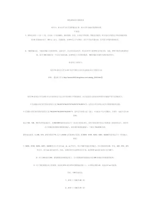
573,574的区别和联系相同点:都可以作为开关量的输出扩展,都可以作为输出数据锁存器。
区别是:1、573是从低-》高-》低,在从高-》低的瞬间,锁存数据;但是,在高电平的时候,数据是直通的,所以也可以使用这个特性做缓冲器,把LE直接接高电平;OE是三态门,直接接地;而574是上升沿锁存,而且不具备直通功能,及不能当作缓冲器来使用。
2、138的输出是,当地址的输入有效的时候,是低电平,其它时间是高电平,所以在时序上跟573是不配合的,因此,573不能作为数据锁存器,除非138的输出加一个反向门接到LE;而574是上升沿锁存数据,138的输出直接作为锁存脉冲即可;参见网上分析如下:使用74系列芯片作为I/O并行扩展的方法以及总线驱动芯片的使用方法转贴:【老树工作室/catalog_2005.html】使用74系列芯片作为I/O并行扩展的常见于过去单片机I/O口不够的情况,而且是需要大量的内存和程序存储器严重不足的情况下。
开关量输出的扩展经常使用的芯片是74LS273/74LS373/74LS573/74LS574等;这些芯片的共同特点是具有数据锁存的功能;开关量输入的扩展经常使用的芯片是74LS244/74LS245/74LS240等;这些芯片的特点是三态门,可以把多个芯片的输出,并联在一起而不会互相影响;通过138、139、153等译码选通芯片,把RD/WR/地址的高位信号(高3位或者高4位,看单片机系统中的芯片的数量)接到译码芯片,把译码芯片的输出接到锁存器的锁存输入,或者缓冲器的选通输入。
下面以74LS138为例。
要特别注意到,对245、574、273等使用TTL芯片以RAM方式做I/O扩展的,跟8255、8155、8253、8251、62256等系列芯片不一样的地方,就是:1)8255、8155、8253、8251、62256等芯片本身有wr、rd、ce等信号,所以138的地址译码输出,可以直接接到CE;但是,245、574、273等芯片,没有wr或者rd信号,因此,如果系统中有这样的芯片扩展,就需要把wr或者rd加入到138中;2)对于245或者244,要把数据读到数据总线上,芯片的数据的使能端必须是WR和地址译码数据的混和;3)对于要把数据总线上的数据,锁存到574或者273的数据输出端口上,必须锁存器的LE,是地址和wr的混和;因此,138的接法是:1、A15-》138的A2(3)2、A14-》138的A1(2)3、A13-》138的A0(1)4、RD和WR接74LS00,00的输出接138的E3(6)5、138的输出接245的E或者574的CLK;这样,使用MOVX a,@dptr的时候,才能在245的E上出现带地址的RD信号;使用MOVX @dptr,A的时候,才能在574的CLK上出现带地址的WR信号;参见574的真值表,可见,E应该接低电平;373、573与273、574有所区别:1、573是从低-》高-》低,在从高-》低的瞬间,锁存数据;但是,在高电平的时候,数据是直通的,所以也可以使用这个特性做缓冲器,把LE直接接高电平;OE是三态门,直接接地;2、但是138的输出是,当地址的输入有效的时候,是低电平,其它时间是高电平,所以在时序上跟573是不配合的,因此,573不能作为数据锁存器,除非138的输出加一个反向门接到LE;而574是上升沿锁存数据,138的输出直接作为锁存脉冲即可;如果系统中没有8255、8155、8253、8251、62256这样的芯片,也可以使用139,RD和wr分别接入一个2-4译码器,译码器的输出分别接到245的E和574的LE,这样可以省去一个74LS00。
74HC574应用电路原理图
74HC574应用电路原理图
寄存器是一种重要的数字电路部件, 常用来暂时存放数据、指令等。
一个触发器可以存储一位二进制代码,存放N位二进制代码,用N个触发器即可。
因为我们的模型机是8位的,因此在本模型机中大部分寄存器是8位的,标志位寄存器(Cy, Z)是二位的。
在COP2000实验仪中,寄存器由74HC574构成,它可以存放8位二进制代码,其中的一位二进制代码是由一个D触发器来存储的。
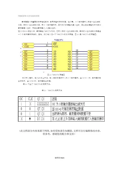
首先,我们先介绍一下74HC574的工作原理。
图2-1是74HC574的原理图。
图2-1 74HC574原理图
我们可以看到,在CLK的上升沿,输入端的数据被打入到8个触发器中。
当OC = 1 时,触发器的输出被关闭,当OC=0时,触发器输出数据。
表2-1列出了74HC574的使用方法。
表2-1 74HC574使用方法
(此文档部分内容来源于网络,如有侵权请告知删除,文档可自行编辑修改内容,
供参考,感谢您的配合和支持)
编辑版word。
74系列芯片功能说明
74系列芯片功能说明(ZZ)作者 AppNotes 日期 2008-2-17 15:15:0074芯片特性分类使总汇74系列集成电路大致可分为6大类:74××(标准型);74LS××(低功耗肖特基);74S××(肖特基);74ALS××(先进低功耗肖特基);74AS××(先进肖特基);74F××(高速)。
近年来还出现了高速CMOS电路的74系列,该系列可分为3大类:HC为COMS工作电平;HCT为TTL工作电平,可与74LS系列互换使用;HCU适用于无缓冲级的CMOS电路。
这9种74系列产品,只要后边的标号相同,其逻辑功能和管脚排列就相同。
用户应根据不同的条件和要求选用不同类型的74系列产品,比如电路的供电电压为3V时就应选择74HC 系列的产品。
系列电平典型传输延迟ns 最大驱动电流(-Ioh/Lol)mA AHC CMOS 8.5 -8/8AHCT COMS/TTL 8.5 -8/8HC COMS 25 -8/8HCT COMS/TTL 25 -8/8ACT COMS/TTL 10 -24/24F TTL 6.5 -15/64ALS TTL 10 -15/64LS TTL 18 -15/24LVCACSLC说明:1)LS是低功耗肖特基,HC是高速COMS;LS的速度比HC略快,HCT输入输出与LS兼容,但是功耗低;F是高速肖特基电路;2)LS是TTL电平,HC是COMS电平;3)LS输入开路为高电平,HC输入不允许开路,HC 一般都要求有上下拉电阻来确定输入端无效时的电平,LS 却没有这个要求;4)LS输出下拉强上拉弱,HC 上拉下拉相同;5)工作电压不同:LS只能用5V,而HC一般为2V到6V;6)电平不同:LS是TTL电平,其低电平和高电平分别为0.8和V2.4,而CMOS在工作电压为5V时分别为0.3V和3.6V,所以CMOS可以驱动T TL,但反过来是不行;7)驱动能力不同:LS一般高电平的驱动能力为5mA,低电平为20mA;而CMOS的高低电平均为5mA;8)CMOS器件抗静电能力差,易发生栓锁问题,所以CMOS的输入脚不能直接接电源。
完整word版74HC573功能说明原创编辑
1锁存器的功74CH5774LS37原理一样数据锁存器。
主要用于数码管、按键等等的控74HC57个脚,数据的进和出没有逻辑关系,这个芯片主要是看高电压激活还是274HC57电压激活是低电压激活芯D7D2~脚是数据的输入脚脚是接1脚是高电压激活芯112~1脚是数据的输出是电20121.真值表意思如下:74HC573真值表,1时,输出端数据等于输入端数据;、LE==?第一行/第二行:当OE0 时,输出端保持不变;=、LE0?第三行:当OE=0 为何,输出端为高阻态;Dn、LE 第四行:当OE=1是无论? 2. 高阻态在这种状态下,可以多而是高阻抗的状态;就是输出既不是高电平,也不是低电平,这些芯片中只能有一个处于非高阻态状态,否则会将芯片烧毁。
高个芯片并联输出;但是,通讯中还可以用到。
RS422 阻态的概念在RS232和数据锁存3.数据仍然保持;这个概念在并行数据扩展中当输入的数据消失时,在芯片的输出端, 经常使用到。
4. 数据缓冲加强驱动能力:74LS244/74LS245/74LS373/74LS573都具备数据缓冲的能力。
,输出使能;:output_enable? OE 是锁存的意思;atch:latch_enable,数据锁存使能,LE?路输入数据;:第n ?Dn 路输出数据;On :第n?23在实际应用的时候是这样做的:74HC573波形图,;OE=0a.;先将数据从单片机的口线上输出到Dnb.从0->1->0 ;c.再将LE 这时,你所需要输出的数据就锁存在On上了,输入的数据在变化也影响不到输d.……单出的数据了;实际上,单片机现在在忙着干别的事情,串行通信、扫描键盘片机的资源有限啊。
这条方式进行并行数据的扩展时RAM,使用movx @dptr, A在单片机按照指令时,这些时序是由单片机来实现的。
因为这些参数都是几后面的表格中还有需要时间的参数,你不需要去管它,的情况下,完12M下的每个指令周期最小是1us十ns级别的,对于单片机在全可以实现;如果是你自己来实现这个逻辑,类似的指令如下:MOV P0,A ; //将数据输出到并行数据端口LE CLRSETB LE的波形从LE ; //上面三条指令完成LE0->1->0的变化CLR数据输入和,,74LS37374LS573跟逻辑上完全一样只不过是管脚定义不一样输出端.3。
HD74BC574A资料
HD74BC574AOctal D Type Flip Flops With 3 State OutputsADE-205-042 (Z)Rev. 0June 1993 DescriptionThe HD74BC574A provides high drivability and operation equal to or better than high speed bipolar standard logic IC by using Bi-CMOS process. The device features low power dissipation that is about 1/5 of high speed bipolar logic IC, when the frequency is 10 MHz. The device has eight edge triger D type flip flops with three state outputs in a 20 pin package. Data at the D inputs meeting set up requirements, are transferred to the Q outputs on positive going transitions of the clock input. When the latch enable goes low, data at the D inputs will be retained at the outputs until latch enable returns high again. When a high logic level is applied to the output control input, all outputs go to a high impedance state, regardless of what signals are present at the other inputs and the state of the strage elements.Features• Input/Output are at high impedance state when power supply is off.• Built in input pull up circuit can make input pins be open, when not used.• TTL level input• Wide operating temperature rangeTa = –40 to + 85°CHD74BC574A2Function TableInputsOutput Control CKD Output QL H HL L L L L X Q 0H X XZH :High level L :Low level X :ImmaterialZ:High impedance: Low to high transition Q 0:Level of Q before the indicated steady state input conditions were established.Pin ArrangementHD74BC574A3Absolute Maximum RatingsItemSymbol Rating Unit Supply voltage V CC –0.5 to +7.0V Input diode current I IK ±30mA Input voltage V IN –0.5 to +7.5V Output voltage V OUT –0.5 to +7.5V Off state output voltage V OUT(off)–0.5 to +5.5V Storage temperature Tstg–65 to +150°CNote:1.The absolute maximum ratings are values which must not individually be exceeded, andfurthermore, no two of which may be realized at the same time.Recommended Operating ConditionsItemSymbol Min Typ Max Unit Supply voltage V CC 4.5 5.0 5.5V Input voltage V IN 0—V CC V Output voltage V OUT 0—V CC V Operating temperature Topr –40—85°C Input rise/fall time*1t r , t f—8ns/VNote:1.This item guarantees maximum limit when one input switches.Waveform: Refer to test circuit of switching characteristics.HD74BC574A Logic Diagram4HD74BC574A5Electrical Characteristics (Ta = –40°C to +85°C)Item Symbol V CC (V)Min Max Unit Test ConditionsInput voltage V IH 2.0—V V IL —0.8V Output voltageV OH 4.5 2.4—V I OH = –3 mA 4.5 2.0—V I OH = –15 mA V OL4.5—0.4V I OL = 24 mA 4.5—0.5V I OL = 48 mA Input diode voltage V IK 4.5—–1.2V I IN = –18 mA Input currentI I5.5—–250µA V IN = 0 V 5.5— 1.0µA V IN = 5.5 V 5.5—100µA V IN = 7.0 V Short circuit output current*1I OS 5.5–100–225mA V IN = 0 or 5.5 V Off state output current I OZH 5.5—50µA V O = 2.7 V I OZL 5.5—–50µA V O = 0.5 V Supply currentI CCL 5.5—29.5mA V IN = 0 or 5.5 V All outputs is “L”I CCH 5.5— 2.5mA V IN = 0 or 5.5 V All outputs is “H”I CCZ 5.5— 2.5mA V IN = 0 or 5.5 V All outputs is “Z”I CCT *25.5—1.5mAV IN = 3.4 or 0.5 V Notes: 1.Not more than one output should be shorted at a time and duration of the short circuit should notexceed one second.2.When input by the TTL level, it shows I CC increase at per one input pin.HD74BC574A6Switching Test Method (C L = 50 pF)Ta = 25°C V CC = 5.0 VTa = –40 to 85°C V CC = 5.0 V ±10%Item SymbolMin Max Min Max Unit Test conditions Propagation CK →Q t PLH3.08.0 3.010.0nsSee under figuredelay time t PHL 3.08.0 3.010.0Output enable time t ZH 3.09.0 3.011.0ns t ZL 3.09.0 3.011.0Output disable time t HZ 3.08.0 3.010.0ns t LZ 3.08.0 3.010.0Setup time t s (H) 2.0— 2.0—ns t s (L) 2.0— 2.0—Hold time t h (H) 2.0— 2.0—ns t h (L) 2.0— 2.0—Pulse width t W (H) 6.0— 6.0—ns t W (L) 6.0—6.0—Input capacitance C IN 3.0 (Typ)——pF V IN = V CC or GND Output capacitanceC O15.0 (Typ)—pFV O = V CC or GNDTest CircuitHD74BC574A Waveforms-1Waveforms-27HD74BC574A8Waveforms-3Notes:1.t r = 2.5 ns, t f = 2.5 ns2.Input waveform: PRR = 1 MHz, duty cycle 50%3.Waveform-A shows input conditions such that the output is “L” level when enable by the output control.4.Waveform-B shows input conditions such that the output is “H” level when enable by the output control.HD74BC574A Package DimensionsUnit: mm9Cautions1.Hitachi neither warrants nor grants licenses of any rights of Hitachi’s or any third party’s patent,copyright, trademark, or other intellectual property rights for information contained in this document.Hitachi bears no responsibility for problems that may arise with third party’s rights, includingintellectual property rights, in connection with use of the information contained in this document.2.Products and product specifications may be subject to change without notice. Confirm that you have received the latest product standards or specifications before final design, purchase or use.3.Hitachi makes every attempt to ensure that its products are of high quality and reliability. However,contact Hitachi’s sales office before using the product in an application that demands especially high quality and reliability or where its failure or malfunction may directly threaten human life or cause risk of bodily injury, such as aerospace, aeronautics, nuclear power, combustion control, transportation,traffic, safety equipment or medical equipment for life support.4.Design your application so that the product is used within the ranges guaranteed by Hitachi particularly for maximum rating, operating supply voltage range, heat radiation characteristics, installationconditions and other characteristics. Hitachi bears no responsibility for failure or damage when used beyond the guaranteed ranges. Even within the guaranteed ranges, consider normally foreseeable failure rates or failure modes in semiconductor devices and employ systemic measures such as fail-safes, so that the equipment incorporating Hitachi product does not cause bodily injury, fire or other consequential damage due to operation of the Hitachi product.5.This product is not designed to be radiation resistant.6.No one is permitted to reproduce or duplicate, in any form, the whole or part of this document without written approval from Hitachi.7.Contact Hitachi’s sales office for any questions regarding this document or Hitachi semiconductor products.Hitachi, Ltd.Semiconductor & Integrated Circuits.Nippon Bldg., 2-6-2, Ohte-machi, Chiyoda-ku, Tokyo 100-0004, Japan Tel: Tokyo (03) 3270-2111 Fax: (03) 3270-5109Copyright ' Hitachi, Ltd., 1999. All rights reserved. Printed in Japan.Hitachi Asia Pte. Ltd.16 Collyer Quay #20-00Hitachi TowerSingapore 049318Tel: 535-2100Fax: 535-1533URLNorthAmerica : http:/Europe : /hel/ecg Asia (Singapore): .sg/grp3/sicd/index.htm Asia (Taiwan): /E/Product/SICD_Frame.htm Asia (HongKong): /eng/bo/grp3/index.htm Japan : http://www.hitachi.co.jp/Sicd/indx.htmHitachi Asia Ltd.Taipei Branch Office3F, Hung Kuo Building. No.167, Tun-Hwa North Road, Taipei (105)Tel: <886> (2) 2718-3666Fax: <886> (2) 2718-8180Hitachi Asia (Hong Kong) Ltd.Group III (Electronic Components)7/F., North Tower, World Finance Centre,Harbour City, Canton Road, Tsim Sha Tsui,Kowloon, Hong Kong Tel: <852> (2) 735 9218Fax: <852> (2) 730 0281 Telex: 40815 HITEC HXHitachi Europe Ltd.Electronic Components Group.Whitebrook ParkLower Cookham Road MaidenheadBerkshire SL6 8YA, United Kingdom Tel: <44> (1628) 585000Fax: <44> (1628) 778322Hitachi Europe GmbHElectronic components Group Dornacher Stra§e 3D-85622 Feldkirchen, Munich GermanyTel: <49> (89) 9 9180-0Fax: <49> (89) 9 29 30 00Hitachi Semiconductor (America) Inc.179 East Tasman Drive,San Jose,CA 95134 Tel: <1> (408) 433-1990Fax: <1>(408) 433-0223For further information write to:。
TEXAS INSTRUMENTS SN54ACT574, SN74ACT574 说明书
SN54ACT574, SN74ACT574OCTAL D-TYPE EDGE-TRIGGERED FLIP-FLOPS WITH 3-STATE OUTPUTS SCAS537D – OCTOBER 1995 – REVISED NOVEMBER 2002D 4.5-V to 5.5-V V CC Operation D Inputs Accept Voltages to 5.5 V D Max t pd of 9 ns at 5 VD Inputs Are TTL-Voltage Compatible description/ordering informationThese 8-bit flip-flops feature 3-state outputsdesigned specifically for driving highly capacitiveor relatively low-impedance loads. The devicesare particularly suitable for implementing bufferregisters, I/O ports, bidirectional bus drivers, andworking registers.The eight flip-flops of the ’ACT574 devices areD-type edge-triggered flip-flops. On the positivetransition of the clock (CLK) input, the Q outputsare set to the logic levels set up at the data (D)inputs.A buffered output-enable (OE) input can be usedto place the eight outputs in either a normal logicstate (high or low logic levels) or thehigh-impedance state. In the high-impedancestate, the outputs neither load nor drive the buslines significantly. The high-impedance state andthe increased drive provide the capability to drivebus lines in a bus-organized system without needfor interface or pullup components.OE does not affect internal operations of the flip-flop. Old data can be retained or new data can be entered while the outputs are in the high-impedance state.To ensure the high-impedance state during power up or power down, OE should be tied to V CC through a pullup resistor; the minimum value of the resistor is determined by the current-sinking capability of the driver.ORDERING INFORMATIONT APACKAGE †ORDERABLE PART NUMBER TOP-SIDE MARKING PDIP – NTube SN74ACT574N SN74ACT574N SOIC DW Tube SN74ACT574DW 40C to 85SOIC – DWTape and reel SN74ACT574DWR ACT574–40°C to 85°C SOP – NSTape and reel SN74ACT574NSR ACT574SSOP – DBTape and reel SN74ACT574DBR AD574TSSOP – PWTape and reel SN74ACT574PWR AD574CDIP – JTube SNJ54ACT574J SNJ54ACT574J –55°C to 125°C CFP – WTube SNJ54ACT574W SNJ54ACT574W LCCC – FK Tube SNJ54ACT574FK SNJ54ACT574FK†Package drawings, standard packing quantities, thermal data, symbolization, and PCB design guidelines areavailable at /sc/package.Copyright 2002, Texas Instruments Incorporated UNLESS OTHERWISE NOTED this docume nt contains PRODUCTION Please be aware that an important notice concerning availability, standard warranty, and use in critical applications of Texas Instruments semiconductor products and disclaimers thereto appears at the end of this data sheet.1234567891020191817161514131211OE 1D 2D 3D 4D 5D 6D 7D 8D GND V CC 1Q 2Q 3Q 4Q 5Q 6Q 7Q 8Q CLK SN54ACT574...J OR W PACKAGE SN74ACT574...DB, DW, N, NS, OR PW PACKAGE (TOP VIEW)32120199101112134567818171615142Q 3Q 4Q 5Q 6Q3D 4D 5D 6D 7D 2D 1D O E 8Q 7Q 1Q 8D G N D C L K V C C SN54ACT574...FK PACKAGE (TOP VIEW)SN54ACT574, SN74ACT574OCTAL D-TYPE EDGE-TRIGGERED FLIP-FLOPS WITH 3-STATE OUTPUTSSCAS537D – OCTOBER 1995 – REVISED NOVEMBER 2002FUNCTION TABLE(each flip-flop)INPUTSOUTPUT OECLK D Q L↑H H L↑L L LH or L X Q 0H X X Z logic diagram (positive logic)OECLK 1D 1QTo Seven Other Channels1D C1111219absolute maximum ratings over operating free-air temperature range (unless otherwise noted)†Supply voltage range, V CC –0.5 V to 7 V . . . . . . . . . . . . . . . . . . . . . . . . . . . . . . . . . . . . . . . . . . . . . . . . . . . . . . . . . . Input voltage range, V I (see Note 1) –0.5 V to V CC + 0.5 V . . . . . . . . . . . . . . . . . . . . . . . . . . . . . . . . . . . . . . . . . . . Output voltage range, V O (see Note 1) –0.5 V to V CC + 0.5 V . . . . . . . . . . . . . . . . . . . . . . . . . . . . . . . . . . . . . . . . Input clamp current, I IK (V I < 0 or V I > V CC) ±20 mA . . . . . . . . . . . . . . . . . . . . . . . . . . . . . . . . . . . . . . . . . . . . . . . . Output clamp current, I OK (V O < 0 or V O > V CC) ±20 mA . . . . . . . . . . . . . . . . . . . . . . . . . . . . . . . . . . . . . . . . . . . . Continuous output current, I O (V O = 0 to V CC ) ±50 mA . . . . . . . . . . . . . . . . . . . . . . . . . . . . . . . . . . . . . . . . . . . . . . Continuous current through V CC or GND ±200 mA . . . . . . . . . . . . . . . . . . . . . . . . . . . . . . . . . . . . . . . . . . . . . . . . . . Package thermal impedance, θJA (see Note 2):DB package 70°C/W. . . . . . . . . . . . . . . . . . . . . . . . . . . . . . . . . DW package 58°C/W. . . . . . . . . . . . . . . . . . . . . . . . . . . . . . . . . N package 69°C/W. . . . . . . . . . . . . . . . . . . . . . . . . . . . . . . . . . . NS package 60°C/W. . . . . . . . . . . . . . . . . . . . . . . . . . . . . . . . . PW package 83°C/W. . . . . . . . . . . . . . . . . . . . . . . . . . . . . . . . . Storage temperature range, T stg –65°C to 150°C . . . . . . . . . . . . . . . . . . . . . . . . . . . . . . . . . . . . . . . . . . . . . . . . . . . †Stresses beyond those listed under “absolute maximum ratings ” may cause permanent damage to the device. These are stress ratings only, and functional operation of the device at these or any other conditions beyond those indicated under “recommended operating conditions ” is not implied. Exposure to absolute-maximum-rated conditions for extended periods may affect device reliability.NOTES: 1.The input and output voltage ratings may be exceeded if the input and output current ratings are observed.2.The package thermal impedance is calculated in accordance with JESD 51-7.SN54ACT574, SN74ACT574OCTAL D-TYPE EDGE-TRIGGERED FLIP-FLOPSWITH 3-STATE OUTPUTSSCAS537D – OCTOBER 1995 – REVISED NOVEMBER 2002 recommended operating conditions (see Note 3)SN54ACT574SN74ACT574MIN MAX MIN MAXUNITV CC Supply voltage 4.5 5.5 4.5 5.5VV IH High-level input voltage22VV IL Low-level input voltage0.80.8VV I Input voltage0V CC0V CC VV O Output voltage0V CC0V CC VI OH High-level output current–24–24mAI OL Low-level output current2424mA∆t/∆v Input transition rise or fall rate88ns/VT A Operating free-air temperature–55125–4085°C NOTE 3:All unused inputs of the device must be held at V CC or GND to ensure proper device operation. Refer to the TI application report Implications of Slow or Floating CMOS Inputs, literature number SCBA004.electrical characteristics over recommended operating free-air temperature range (unless otherwise noted)TEST CONDITIONS CC T A = 25°C SN54ACT574SN74ACT574PARAMETER TEST CONDITIONS VMIN TYP MAX MIN MAX MIN MAXUNITI=504.5 V 4.4 4.49 4.4 4.4OH = –50 µA5.5 V 5.4 5.49 5.4 5.4V OH I=24mA 4.5 V 3.86 3.7 3.76OH = –24 mA5.5 V 4.86 4.7 4.76V I OH = –50 mA† 5.5 V 3.85I OH = –75 mA† 5.5 V 3.85I=50µA 4.5 V0.10.10.1OL = 505.5 V0.10.10.1OL=24mA 4.5 V0.360.440.44V I OL = 24 mA5.5 V0.360.440.44VI OL = 50 mA† 5.5 V 1.65I OL = 75 mA† 5.5 V 1.65I OZ V O = V CC or GND 5.5 V±0.25±5±2.5µA I I V I = V CC or GND 5.5 V±0.1±1±1µA I CC V I = V CC or GND,I O = 0 5.5 V48040µA∆I CC‡One input at 3.4 V,Other inputs at GND or V CC5.5 V0.6 1.5 1.5mAC i V I = V CC or GND 5 V 4.5pF †Not more than one output should be tested at a time, and the duration of the test should not exceed 2 ms.‡This is the increase in supply current for each input that is at one of the specified TTL voltage levels, rather than 0 V or V CC.PRODUCT PREVIEW information concerns products in the formative orSN54ACT574, SN74ACT574OCTAL D-TYPE EDGE-TRIGGERED FLIP-FLOPS WITH 3-STATE OUTPUTSSCAS537D – OCTOBER 1995 – REVISED NOVEMBER 2002timing requirements over recommended operating free-air temperature range, V CC = 5 V ±0.5 V (unless otherwise noted) (see Figure 1)T A = 25°CSN54ACT574SN74ACT574MIN MAXMIN MAX MIN MAX UNIT f clockClock frequency 1007085MHz t wPulse duration, CLK high or low 354ns t suSetup time, data before CLK ↑ 2.5 3.5 2.5ns t h Hold time, data after CLK ↑121ns switching characteristics over recommended operating free-air temperature range,V CC = 5 V ±0.5V (unless otherwise noted) (see Figure 1)FROM TO T A = 25°C SN54ACT574SN74ACT574PARAMETER(INPUT)(OUTPUT)MIN TYP MAX MIN MAX MIN MAX UNIT f max1001107085MHz t PLH2.5711 1.513.5212t PHLCLK Q 2 6.510 1.512.5 1.511ns t PZH2 6.49.5 1.511 1.510t PZLOE Q 269 1.511 1.510ns t PHZ2710.5 1.512 1.511.5t PLZ OE Q 2 5.58.5 1.510 1.59nsoperating characteristics, V CC = 5 V, T A = 25°CPARAMETERTEST CONDITIONS TYP UNIT C pd Power dissipation capacitance C L = 50 pF, f = 1 MHz 40pF PRODUCT PREVIEW information concerns products in the formative orSN54ACT574, SN74ACT574OCTAL D-TYPE EDGE-TRIGGERED FLIP-FLOPS WITH 3-STATE OUTPUTS SCAS537D – OCTOBER 1995 – REVISED NOVEMBER 2002PARAMETER MEASUREMENT INFORMATION50% V CC 3 V3 V 0 V 0 V t h t suVOLTAGE WAVEFORMS Data Input t PLH t PHL V OH V OL3 V 0 V Input Output Timing Input50% V CC From Output Under Test C L = 50 pF(see Note A)LOAD CIRCUITS1 2 × V CC500 Ω500 ΩOutput Control(low-levelenabling)OutputWaveform 1S1 at 2 × V CC (see Note B)OutputWaveform 2S1 at Open(see Note B)V OL V OH t PZL t PZH t PLZ t PHZ ≈V CC 0 V 50% V CC V OL + 0.3 V 50% V CC≈0 V Open VOLTAGE WAVEFORMS t PLH /t PHLt PLZ /t PZLt PHZ /t PZH Open 2 × V CC Open TEST S13 V0 Vt wVOLTAGE WAVEFORMS Input V OH – 0.3 V 3 V NOTES: A.C L includes probe and jig capacitance.B.Waveform 1 is for an output with internal conditions such that the output is low except when disabled by the output control.Waveform 2 is for an output with internal conditions such that the output is high except when disabled by the output control.C.All input pulses are supplied by generators having the following characteristics:PRR ≤ 1 MHz, Z O = 50 Ω, t r ≤ 2.5 ns, t f ≤ 2.5 ns.D.The outputs are measured one at a time with one input transition per measurement.VOLTAGE WAVEFORMS 1.5 V 1.5 V1.5 V 1.5 V 1.5 V 1.5 V 1.5 V 1.5 V 1.5 V Figure 1. Load Circuit and Voltage WaveformsPACKAGING INFORMATIONOrderable Device Status(1)PackageType PackageDrawingPins PackageQtyEco Plan(2)Lead/Ball Finish MSL Peak Temp(3)SN74ACT574DBLE OBSOLETE SSOP DB20TBD Call TI Call TISN74ACT574DBR ACTIVE SSOP DB202000Pb-Free(RoHS)CU NIPDAU Level-2-260C-1YEAR/Level-1-235C-UNLIMSN74ACT574DBRE4ACTIVE SSOP DB202000Pb-Free(RoHS)CU NIPDAU Level-2-260C-1YEAR/Level-1-235C-UNLIMSN74ACT574DW ACTIVE SOIC DW2025Pb-Free(RoHS)CU NIPDAU Level-2-250C-1YEAR/Level-1-235C-UNLIMSN74ACT574DWE4ACTIVE SOIC DW2025Pb-Free(RoHS)CU NIPDAU Level-2-250C-1YEAR/Level-1-235C-UNLIMSN74ACT574DWR ACTIVE SOIC DW202000Pb-Free(RoHS)CU NIPDAU Level-2-250C-1YEAR/Level-1-235C-UNLIMSN74ACT574DWRE4ACTIVE SOIC DW202000Pb-Free(RoHS)CU NIPDAU Level-2-250C-1YEAR/Level-1-235C-UNLIMSN74ACT574N ACTIVE PDIP N2020Pb-Free(RoHS)CU NIPDAU Level-NC-NC-NCSN74ACT574NSR ACTIVE SO NS202000Pb-Free(RoHS)CU NIPDAU Level-2-260C-1YEAR/Level-1-235C-UNLIMSN74ACT574NSRE4ACTIVE SO NS202000Pb-Free(RoHS)CU NIPDAU Level-2-260C-1YEAR/Level-1-235C-UNLIMSN74ACT574PW ACTIVE TSSOP PW2070Pb-Free(RoHS)CU NIPDAU Level-1-250C-UNLIMSN74ACT574PWE4ACTIVE TSSOP PW2070Pb-Free(RoHS)CU NIPDAU Level-1-250C-UNLIMSN74ACT574PWG4ACTIVE TSSOP PW2070Green(RoHS&no Sb/Br)CU NIPDAU Level-1-260C-UNLIM SN74ACT574PWLE OBSOLETE TSSOP PW20TBD Call TI Call TISN74ACT574PWR ACTIVE TSSOP PW202000Pb-Free(RoHS)CU NIPDAU Level-1-250C-UNLIMSN74ACT574PWRE4ACTIVE TSSOP PW202000Pb-Free(RoHS)CU NIPDAU Level-1-250C-UNLIMSN74ACT574PWRG4ACTIVE TSSOP PW202000Green(RoHS&no Sb/Br)CU NIPDAU Level-1-260C-UNLIM(1)The marketing status values are defined as follows:ACTIVE:Product device recommended for new designs.LIFEBUY:TI has announced that the device will be discontinued,and a lifetime-buy period is in effect.NRND:Not recommended for new designs.Device is in production to support existing customers,but TI does not recommend using this part in a new design.PREVIEW:Device has been announced but is not in production.Samples may or may not be available.OBSOLETE:TI has discontinued the production of the device.(2)Eco Plan-The planned eco-friendly classification:Pb-Free(RoHS)or Green(RoHS&no Sb/Br)-please check /productcontent for the latest availability information and additional product content details.TBD:The Pb-Free/Green conversion plan has not been defined.Pb-Free(RoHS):TI's terms"Lead-Free"or"Pb-Free"mean semiconductor products that are compatible with the current RoHS requirements for all6substances,including the requirement that lead not exceed0.1%by weight in homogeneous materials.Where designed to be soldered at high temperatures,TI Pb-Free products are suitable for use in specified lead-free processes.Green(RoHS&no Sb/Br):TI defines"Green"to mean Pb-Free(RoHS compatible),and free of Bromine(Br)and Antimony(Sb)based flame retardants(Br or Sb do not exceed0.1%by weight in homogeneous material)(3)MSL,Peak Temp.--The Moisture Sensitivity Level rating according to the JEDEC industry standard classifications,and peak solder temperature.Important Information and Disclaimer:The information provided on this page represents TI's knowledge and belief as of the date that it is provided.TI bases its knowledge and belief on information provided by third parties,and makes no representation or warranty as to the accuracy of such information.Efforts are underway to better integrate information from third parties.TI has taken and continues to take reasonable steps to provide representative and accurate information but may not have conducted destructive testing or chemical analysis on incoming materials and chemicals.TI and TI suppliers consider certain information to be proprietary,and thus CAS numbers and other limited information may not be available for release.In no event shall TI's liability arising out of such information exceed the total purchase price of the TI part(s)at issue in this document sold by TI to Customer on an annual basis.MECHANICAL DATAMSSO002E – JANUARY 1995 – REVISED DECEMBER 2001DB (R-PDSO-G**)PLASTIC SMALL-OUTLINE4040065/E 12/0128 PINS SHOWNGage Plane8,207,400,550,950,253812,9012,302810,50248,50Seating Plane9,907,903010,509,900,385,605,00150,2214A28120166,506,50140,05 MIN5,905,90DIM A MAXA MIN PINS **2,00 MAX6,907,500,65M0,150°–ā8°0,100,090,25NOTES: A.All linear dimensions are in millimeters.B.This drawing is subject to change without notice.C.Body dimensions do not include mold flash or protrusion not to exceed 0,15.D.Falls within JEDEC MO-150MECHANICAL DATAMTSS001C – JANUARY 1995 – REVISED FEBRUARY 1999PW (R-PDSO-G**)PLASTIC SMALL-OUTLINE PACKAGE14 PINS SHOWN0,65M0,100,100,250,500,750,15 NOMGage Plane289,809,60247,907,7020166,606,404040064/F 01/970,306,606,2080,194,304,5070,1514A11,20 MAX145,104,9083,102,90A MAXA MIN DIM PINS **0,054,905,10Seating Plane0°–8°NOTES: A.All linear dimensions are in millimeters.B.This drawing is subject to change without notice.C.Body dimensions do not include mold flash or protrusion not to exceed 0,15.D.Falls within JEDEC MO-153IMPORTANT NOTICETexas Instruments Incorporated and its subsidiaries (TI) reserve the right to make corrections, modifications, enhancements, improvements, and other changes to its products and services at any time and to discontinue any product or service without notice. Customers should obtain the latest relevant information before placing orders and should verify that such information is current and complete. All products are sold subject to TI’s terms and conditions of sale supplied at the time of order acknowledgment.TI warrants performance of its hardware products to the specifications applicable at the time of sale in accordance with TI’s standard warranty. T esting and other quality control techniques are used to the extent TI deems necessary to support this warranty. Except where mandated by government requirements, testing of all parameters of each product is not necessarily performed.TI assumes no liability for applications assistance or customer product design. Customers are responsible for their products and applications using TI components. T o minimize the risks associated with customer products and applications, customers should provide adequate design and operating safeguards.TI does not warrant or represent that any license, either express or implied, is granted under any TI patent right, copyright, mask work right, or other TI intellectual property right relating to any combination, machine, or process in which TI products or services are used. Information published by TI regarding third-party products or services does not constitute a license from TI to use such products or services or a warranty or endorsement thereof. Use of such information may require a license from a third party under the patents or other intellectual property of the third party, or a license from TI under the patents or other intellectual property of TI.Reproduction of information in TI data books or data sheets is permissible only if reproduction is without alteration and is accompanied by all associated warranties, conditions, limitations, and notices. Reproduction of this information with alteration is an unfair and deceptive business practice. TI is not responsible or liable for such altered documentation.Resale of TI products or services with statements different from or beyond the parameters stated by TI for that product or service voids all express and any implied warranties for the associated TI product or service and is an unfair and deceptive business practice. TI is not responsible or liable for any such statements. Following are URLs where you can obtain information on other Texas Instruments products and application solutions:Products ApplicationsAmplifiers Audio /audioData Converters Automotive /automotiveDSP Broadband /broadbandInterface Digital Control /digitalcontrolLogic Military /militaryPower Mgmt Optical Networking /opticalnetwork Microcontrollers Security /securityTelephony /telephonyVideo & Imaging /videoWireless /wirelessMailing Address:Texas InstrumentsPost Office Box 655303 Dallas, Texas 75265Copyright 2005, Texas Instruments Incorporated。