pcb的caf标准
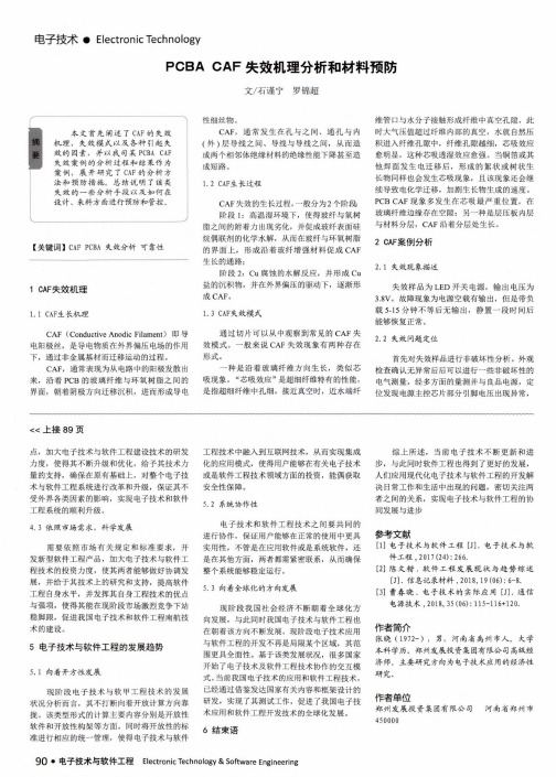
PCBA CAF失效机理分析和材料预防
通过切片可以从中观察到常见的CAF失 效模式。一般来说CAF失效现象有两种存在 形式。
一种是沿着玻璃纤维方向生长,类似芯 吸现象。'‘芯吸效应”是超细纤维特有的性能, 是指超细纤维中孔细,接近真空时,近水端纤
维管口与水分子接触形成纤维中真空孔隙,此 时大气压值超过纤维内部的真空,水就自然压 积进入纤维孔隙中,纤维孔隙越细,芯吸效应 愈明显,这种芯吸透湿效应愈强。当铜箔或其 他焊面发生电迁移后,形成的絮状或树状生 长物同样也会发生芯吸现象,且该现象还会继 续导致电化学迁移,加剧生长物生成的速度。 PCB CAF现象多发生在芯吸最严重位置,在 玻璃纤维边缘存在空隙;另一种是层压板内层 与材料分层,CAF沿着分层处生长。
性细丝物。 CAF,通常发生在孔与之间、通孔与内
(外)层导线之间、导线与导线之间,从而造 成两个相邻体绝缘材料的绝缘性能下降甚至造 成短路。
1. 2 CAF生长过程
CAF失效的生长过程,一般分为2个阶段 阶段1:高温湿环境下,使得玻纤与氧树 脂之间的附着力出现劣化,并促成玻纤表面硅 烷偶联剂的化学水解,从而在玻纤与环氧树脂 的界面上,形成沿着玻纤增强材料促成CAF 生长的通路; 阶段2: Cu腐蚀的水解反应,并形成Cu 盐的沉积物,并在外界偏压的驱动下,逐渐形 成 CAFo
5电子技术与软件工程的发展趋势
5. 1向着开方性发展
现阶段电子技术与软甲工程技术的发展 状况分析而言,其不打断向着开放计算方向靠 拢。该类型形式的计算主要内容分别是开放性 软件和开放性构架等方面。同时将开放性的标 准进行相应的统一管理,使得电子技术与软件
工程技术中融入到互联网技术,从而实现集成 化的应用模式,使得用户能够在有关电子技术 或是软件工程技术领域方面的投资,能偶获取 安全性保障。
CAF的成因及检测

覆铜板玻纤纱漏电之探讨2008-11-28 14:45:55 资料来源:PCBcity 作者: 白蓉生一、无风不起浪,事出必有因传统钻孔镀孔后其相邻通孔铜壁之间,必定会出现玻纤纱束彼此之搭连(Hole to Hole;H/H),甚至当相邻两导线之根部恰巧踩在同一束玻纤纱上(Trace to Trace;T/T),或导线之根部与孔壁之间经过玻纤纱的接(T/H),又或者层与层之间(L/L)经由玻纤纱沟通等潜在病灶。
当使用环境堪称良好时,其两点之间尚能维持足够之绝缘(即绝缘电阻要够高),而不致影响到传输线中工作能量的漏失。
然而一旦出现高温高湿之恶劣环境,而板材品质又不是很好,且两点间之电压又出现差异(偏压Bias)之影响下,时间一久难免就会发病,而且在腐蚀后会出现铜离子,当其沿着玻纤束发生缓慢的迁移动作,进而出现轻微之漏电行为者,特称为CAF(Conductive Anodic Filament),如Isola所绘制的下三图。
图1此为台湾Isola公司所提供CAF Growth(红色部份) 的示意图与原文之内容说明,对CAF 发生经过之了解颇有助益。
不过目前台湾覆铜板业者所进行之CAF试验皆为日式规格,并非美式之高阶规格者,且IPC亦尚未具备整体之试验方法。
由于讯号传输的速度不断加快,及为减少发热起见,电子产品所设定的工作电压已不断降低(由30年前的12V,到20年前的5V,到今日的1.5V,甚至数年后之1V以下),通常PCB 之导体或板材难免都会存在少许瑕疵,也难免会带来轻微杂讯(Noise),然而此等芝麻绿豆的小事,当年根本未放在眼里。
时至高速传输的今日,小小微恙却在高阶板类中几乎成了心腹大患,必尽除之而后已!是故大哥大的基地台、发射总台、电脑网路的路由器( Router)、大型电脑的枢纽机站等,其高层数厚大背板(High Layer count)之板材,必须避免或减少CAF发生的机率,而令大型机组长期(如20年)使用中的可靠度(Reliability) 方得以确保。
PCB 耐温与无铅标准

RoHS & Lead Free对PCB之冲击于2006年7月1日起欧盟开始实施之RoHS立法,虽然欧洲与j本PCB厂商已展开各项Lead Free制程与材料切换,并如火如荼的进行测试。
但若干本土的PCB厂因主要订单在美商,基于成本的考量,仍采取观望的态度。
但如果不正视此问题,一旦美系OEM、EMS大厂决定跟进,必将措手不及衍生出诸多问题,可能的冲击不可等闲视之。
▲FR-4树脂、铜箔、焊料与背动元件彼此存在热胀系数之差异,其中树脂Z方向的热胀系数高达60ppm/℃,与其它三者差异甚大。
由于锡铅焊接之组装方式已沿用40年以上,不但可靠度佳且上至材料下至制程参数与设备均十分成熟,且过去发生的信赖性问题与因应对策已建立完整的资料库,故发生客诉时,可迅速厘清责任归属。
但进入Lead Free时代,从上游材料、PCB表面处理、组装之焊料、设备等与以往大相迳庭,且大家均无使用的经验值,一旦产生问题,除责任不易归属外,后续衍生丢失订单、天价索赔的问题可能层出不穷,故不可不慎。
Lead Free组装通用的焊料锡银铜合金(SAC),其熔点、熔焊(Reflow)温度、波焊(Wave Soldering)温度分别较锡铅合金高15℃35℃以上,几乎是目前 FR-4板材耐热的极限。
再加上重工的考量,以现有板材因应无铅制程存在相当的风险。
有监于此,美国电路板协会(IPC)乃成立基板材料之委员会,针对无铅制程的要求订定新规范。
然而,无铅时代面临产业上、下游供应链的重新洗牌,委员会各成员基于其所代表公司利益的考量,不得不作若干妥协。
最后协调出的版本,似乎尽能达到最低标准。
因此,即使通过 IPC规范,并不代表实务面不会发生问题,使用者仍需根据自身的需求仔细研判。
以新版IPC-4101B而言,有几个重要参数:Tg(板材玻璃转化温度):可分一般Tg(110℃150℃),中等Tg(150℃170℃),High Tg(>170℃)以上三大类。
PCB耐热裂与无铅标准概述

RoHS & Lead Free对PCB之冲击于2006年7月1日起欧盟开始实施之RoHS立法,虽然欧洲与j本PCB厂商已展开各项Lead Free制程与材料切换,并如火如荼的进行测试。
但若干本土的PCB厂因主要订单在美商,基于成本的考量,仍采取观望的态度。
但如果不正视此问题,一旦美系OEM、EMS大厂决定跟进,必将措手不及衍生出诸多问题,可能的冲击不可等闲视之。
▲FR-4树脂、铜箔、焊料与背动元件彼此存在热胀系数之差异,其中树脂Z方向的热胀系数高达60ppm/℃,与其它三者差异甚大。
由于锡铅焊接之组装方式已沿用40年以上,不但可靠度佳且上至材料下至制程参数与设备均十分成熟,且过去发生的信赖性问题与因应对策已建立完整的资料库,故发生客诉时,可迅速厘清责任归属。
但进入Lead Free时代,从上游材料、PCB表面处理、组装之焊料、设备等与以往大相迳庭,且大家均无使用的经验值,一旦产生问题,除责任不易归属外,后续衍生丢失订单、天价索赔的问题可能层出不穷,故不可不慎。
Lead Free组装通用的焊料锡银铜合金(SAC),其熔点、熔焊(Reflow)温度、波焊(Wave Soldering)温度分别较锡铅合金高15℃35℃以上,几乎是目前 FR-4板材耐热的极限。
再加上重工的考量,以现有板材因应无铅制程存在相当的风险。
有监于此,美国电路板协会(IPC)乃成立基板材料之委员会,针对无铅制程的要求订定新规范。
然而,无铅时代面临产业上、下游供应链的重新洗牌,委员会各成员基于其所代表公司利益的考量,不得不作若干妥协。
最后协调出的版本,似乎尽能达到最低标准。
因此,即使通过IPC规范,并不代表实务面不会发生问题,使用者仍需根据自身的需求仔细研判。
以新版IPC-4101B而言,有几个重要参数:Tg(板材玻璃转化温度):可分一般Tg(110℃150℃),中等Tg(150℃170℃),High Tg (>170℃)以上三大类。
CAF线路板

CAF 等级
通常PCB厂应根据自身制程能力及风险承 通常PCB厂应根据自身制程能力及风险承 受能力制定CAF等级标准 受能力制定CAF等级标准 1、A级—极度风险(例如:孔间隙15mil以 极度风险(例如:孔间隙15mil以 下) 2、B级---高度风险(例如:空间隙15---高度风险(例如:空间隙1525mil) 25mil) 3、C级---有风险(例如:孔间隙25-33mil) ---有风险(例如:孔间隙25-33mil)
如何应对客户无CAF要求,但是客 如何应对客户无CAF要求,但是客 户设计处于风险区域范围?
讨论
如何应对客户无CAF要求,但是客 如何应对客户无CAF要求,但是客 户设计处于风险区域范围?
/PcbInfo/Articl es/2008-12/0812191404084662es/2008-12/0812191404084662-1.htm /questionDetail.do?id= 8034
11必须按照风险等级评估知会客户该钻孔必须按照风险等级评估知会客户该钻孔边到钻孔边设计存在边到钻孔边设计存在cafcaf风险并需要得风险并需要得到客户的到客户的cafcaf让步文件让步文件22使用使用cafcaf物料及流程物料及流程如何应对客户无如何应对客户无cafcaf要求但是客要求但是客户设计处于风险区域范围
二、流程工艺问题 1、孔粗---钻孔太过粗糙,造成玻纤束 被拉松或分离而出现间隙; 2、除胶渣---PCB制程之PTH中的除胶 、除胶渣---PCB制程之PTH中的除胶 渣(Desmearing)过度,或沉铜浸入玻纤 渣(Desmearing)过度,或沉铜浸入玻纤 束发生灯芯效应(Wicking) 束发生灯芯效应(Wicking) ,过度的灯芯加 上孔与孔相距太近时,可能会使得其间板 材的绝缘品质变差 加速产生CAF效应;
PCB板防CAF知识的介绍

第二部分:CAF产生机理和过程
n CAF形成的条件
(1)线路间有电势差,提供了离子运动的动力; (2)有材料间隙的存在,提供了离子运动的通道; (3)有水分的存在,提供了离子化的环境媒介; (4)有金属离子物质的存在。
4
第三部分:影响CAF形成的因素
n 四因素
(1).基材的选择 现在业界经常使用的G-10(一种非阻燃的环氧玻璃布材料)、聚酰亚胺材料(PI)、β-三氮 树脂(BT)、氰酸酯(CE)、环氧玻璃纤维布(FR-4)、CEM3(一种非阻燃的短切毡玻璃材 料)、MC-2(一种混合的聚酯和环氧玻璃板)、Epoxy/Kevlar。各种材料形成CAF的敏感 性程度如下:
6
第四部分:CAF对产品的影响
n 案例二
(1).案例描述 某一款手机产品在出厂和使用初期使用正常,但3-4月份(此为南方一年中最潮湿月份) 在南方维修中心收到大量客户投诉,反应手机按键6、7、8同时出现自动拨号现象。 (2)问题分析 电测发现6、7、8键的信号输出端和输入端均不存在短路,且电路分析还发现这3个键的 公共节点与信号控制芯片的外部电路上某电阻R之间的 绝缘值明显低于正常品,三键的 埋孔及与电阻的埋孔相距很近,这两埋孔的电路输出波形图较正常品异常,故断定该两 孔之间可能存在短路。对两埋孔做金相切片,发现两孔之间严重的铜迁移现象,并使两 镀孔处于短路状态。同时还发现有芯吸、玻纤之间有较大余隙
(1)Cu→Cu2+ +2e-(铜在阳极发生溶解) H2O→H+ + OH- (水分子在阴极发生还原形成OH- ) 2H+ + 2e-→H2
(2)Cu2+ + 2OH- → Cu(OH)2 ( Cu2+、 OH-分别从两极迁移,发生 中和反应形成)
CAF阳极离子迁移

CAF阳极离子迁移原理:由于PCB基材的绝缘层是由树脂与玻璃布所构成,当在高电压状态下,通孔与通孔、线路与线路、线路与通孔间形成一个电场,而PCB湿制程很多,水分中或板面清洁不良残留的电解质可能经由钻孔产生的微裂缝顺着玻璃纤的方向迁移产生短路,造成绝缘失效,这种现象称为CAF阳极性玻纤丝的漏电现象。
CAF测试通过监控测试单元的电阻,当CAF 发生时,绝缘层的绝缘性能下降,电阻也随之下降,由此可判断CAF的失效。
测试标准:IPC-TM-650 2.6.25模块要求:1. IPC-9253和IPC-9254 A1-A4测试结构10层板,尺寸大约125*175mm。
测试板需要为CAF测试钻不同孔壁间距的孔。
这些距离可以低到0.15mm,为了有很高的阻抗阳极离子迁移和最小的镀通孔灯芯;距离最大可以达到0.89mm,用来测试压合的程序。
钻孔的大小在图表中有规定来保持一致的间距。
测试板的玻纤方向应该与同网络的A1-A4的测试孔垂直。
测试板的设计需要有足够的外层空间保证不会出现表面绝缘的失效。
A1-A4每组有5排导通的通孔。
每组中有42个通孔,有的连接到阳极,有的连接到阴极。
通过在不同组或环状通孔间,使用不同的刀径钻同样的1mm,来保持每个结构中的孔边间距不同。
除了钻孔用的刀大小不一致和一些盘的小改动之外,4个结构是一样的。
这4个结构A1-A4通过玻璃纤维连接在一起。
因为A1-A4容易在一个方向上发生阳极离子迁移,所以测试板的玻纤方向应该与同网络的测试孔垂直。
A和B测试结构中,内层和外层的盘是一样的,在给定的测试结构中,盘的大小通常是一样的,虽然在每个结构中都会变化。
所有第2层中电导通的通孔在第9层中重复出现,所以单层的蚀刻不会造成影响。
孔与电极的连接在内层而不是在外层,来降低外层绝缘失效的可能性。
图1两种CAF测试版的设计表1A1-A4结构设计规则2. IPC-9253和IPC-9254 B1-B4测试结构4个B测试结构中,有7组交互的通孔。
CAF---的测试方法

1ScopeThis test method provides a means to assess the propensity for conductive anodic filament(CAF)growth,a form of elec-trochemical migration within a printed wiring board(PWB). Conductive anodic filaments may be composed of conductive salts,rather than cationic metal ions,however inadequate dielectric for the applied voltage,component failures,and part use exceeding the maximum operating temperature(MOT)of the laminate can contribute to product failures as well.This test method can be used to assess PWB laminate materials, PWB design and application parameters,PWB manufacturing process changes and press-fit connector applications.2Applicable Documents2.1IPCIPC-A-47Composite Test Pattern Ten-Layer PhototoolIPC-2221Generic Standard On Printed Board DesignIPC-9253CAF Test Board(Available in the‘Drafts’section of the5-32e Committee Home Page)IPC-9254CAF Test Board(Available in the‘Drafts’section of the5-32e Committee Home Page)IPC/EIA J-STD-001Requirements for Soldered Electrical and Electronic AssembliesJ-STD-004Requirements for Soldering FluxesIPC/EIA J-STD-006,Requirements for Electronic Grade Sol-der Alloys and Fluxed and Non-Fluxed Solid Solders for Elec-tronic Soldering Applications2.2American Society for Testing and Materials(ASTM) ASTM D-257Standard Test Methods for DC Resistance or Conductance of Insulating Materials3Test Specimens(Recommended that the latest version of the CAF test board be used)3.1IPC-9253and IPC-9254The IPC-9253and IPC-9254 have10layers and dimensions are approximately125x175 mm[nominally5x7in].Test board designs for evaluating CAF resistance shall have varying drilled hole wall to drilled hole wall distances for plated holes.These distances can range from as low as0.15mm[0.00591in]separation for alternate laminate materials expected to have very high CAF resistance and minimal copper wicking out from the plated-through hole (PTH),to as high as0.89mm[0.0350in]separation for evalu-ating press-fit connector applications.The drilled hole size, rather than the finished hole size,is specified in the chart on the bare board fabrication drawing to ensure consistent spac-ing.Internal layer thieving may be added to plane layers around the perimeter.Test boards should be manufactured so that the machine/grain direction of the woven fiber rein-forcement is perpendicular to the rows of same-net daisy chain vias for A1-A4(machine/grain direction tends to fail first). Test board designs shall have sufficient minimum spacings on outer layers to ensure that surface insulation resistance fail-ures do not youts of the IPC-9253and IPC-9254 test board structures(CAF Test Boards)are shown below (Figure1).IPC-9253and IPC-9254Test Structures A1through A4The four structures A1-A4each have five rows of connected vias.Within each structure each row has42vias with alternat-ing rows being tied to positive or negative electrodes.The via edge to via edge spacing is varied from one structure to the next by using a different drilled hole size on the same1mm [0.040in]pitch between rows of daisy chain vias.The result-ing via edge to via edge spacings are:0.27mm,0.38mm, 0.51mm,0.65mm[0.0106in,0.0150in,0.0201in,0.0256 in].Other than the use of different drilled hole sizes and a small change in pad sizes,the four structures are identical.The vias in these four test structures A1-A4are aligned with the glass fibers.Since A1-A4evaluate susceptibility to CAF in just one direction,test coupons should be manufactured so that the machine direction of the woven fiber laminate reinforcement is perpendicular to the rows of same-net daisy chain vias (machine direction tends to fail first).For both A and B test structures the inner and outer layer pads are the same,i.e.,the same pad size is consistently used within a given test structure,although it does change from structure to structure.All via to electrode connections are made on layer2and are repeated on layer9so that a single etch-out will not affect results.Traces from via to elec-trode are routed on internal layers rather than external layers to minimize potential for surface insulation resistance failure.Material in this Test Methods Manual was voluntarily established by Technical Committees of IPC.This material is advisory onlyand its use or adaptation is entirely voluntary.IPC disclaims all liability of any kind as to the use,application,or adaptation of thisers are also wholly responsible for protecting themselves against all claims or liabilities for patent infringement.Equipment referenced is for the convenience of the user and does not imply endorsement by IPC.Page1of9Design details for each test structure A1-A4follows in Table1. Note:‘‘Manhattan Distance’’is the shortest orthogonal dis-tance along the X-and/or Y-axes lines between adjacent drilled hole features(corresponds to the orthogonal nature of the laminate material’s woven glass fiber reinforcement(Figure 2).IPC-9253and IPC-9254Test Structures B1through B4The four‘‘B’’test structures have seven alternating rows of vias.Within each structure,alternating rows have either27or 26vias with the alternating rows being tied to either positive or negative electrodes.The via edge to via edge spacing isFigure1Layouts of the Two Versions of the CAF Test BoardsTable1Test Structures A1through A4Design RulesA1A2A3A4Outer layer pad size0.86mm[0.0339in]0.81mm[0.0319in]0.75mm[0.0295in]0.69mm[0.0272in] Inner layer pad size0.86mm[0.0339in]0.81mm[0.0319in]0.75mm[0.0295in]0.69mm[0.0272in] Drilled hole size0.74mm[0.0291in]0.63mm[0.0248in]0.51mm[0.0201in]0.37mm[0.0146in] Via edge to via edge(shortest distance)0.27mm[0.0106in]0.38mm[0.0150in]0.51mm[0.0201in]0.65mm[0.0256in] Via edge to via edge(Manhattan Distance)0.27mm[0.0106in]0.38mm[0.0150in]0.51mm[0.0201in]0.65mm[0.0256in]On IPC-9254only,bias applied between:J1,J5J2,J5J3,J5J4,J5Revision Page2of9varied from one structure to the next by using a different drilled hole size on the same1.52mm x1.52mm[0.05984in x0.05984in]via grid.The1.52mm x1.52mm[0.05984in x 0.05984in]grid has an interstitial via therefore,tipping at a 45°angle results in a square1.08mm x1.08mm[0.04252in x0.04252in]grid.Note:the sketches do not look square when tipped45°but,the CAF Test Boards do.The resulting via edge to via edge spacings are:0.26mm,0.37mm,0.51 mm,0.62mm[0.0102in,0.0146in,0.0201in,0.0244in]. Other than the use of different drilled hole sizes and a small change in pad sizes,the four structures are identical.The vias in the‘‘B’’test structure are not aligned with the glass fibers. If the failure mode is along glass bundles it is reasonable to expect the‘‘B’’test structure to perform better than the‘‘A’’structure for equivalent via edge to via edge spacings.Within a given test structure,the inner and outer layer pads for all10 layers are the same,i.e.,the same pad size is consistently used within a given test structure although,it does change from structure to structure.All via to electrode connections are made on layer1and are repeated on layer10so that a single etch-out will not affect results.A conceptual representation of the‘‘B’’test structure is shown to the upper right(Figure3).Design details on each of the four‘‘B’’test structures follows in Table2.3.2Other Structures Section C is designed to evaluate plated-through hole(PTH)-to-plane layer spacings.It is rec-ommended to use the registration coupon F from either test artwork IPC-A-47or IPC-2221when CAF testing includes this region.Section D in the IPC-9254design is for layer-to-layer Z-axis CAF testing.Section D in the IPC-9253is for evaluat-ing CAF resistance in a press-fit compliant pin connector application.The feature in the D region is an optional feature that is present automatically with the design.However,the A, B and C regions shall remain as designed in order to provide a standard basis of comparison.The CAF test board with10layers is designated to evaluate thin single-ply constructions typically used on high perfor-mance boards.This board construction stackup can be reduced down to:(a)four layers by eliminating layers3 through8and(b)only test structures A and B,when just evaluating differences between laminate materials.3.3CAF Test Board Design This10-layer CAF test board for evaluating the insulation resistance between internal con-ductors within a printed wiring board has the following key features for evaluating hole-hole CAF resistance(Figure3).Figure2Manhattan Distance(Shortest Orthogonal)Table2Test Structures B1through B4Design RulesB1B2B3B4Outer layer pad size0.94mm[0.0370in]0.89mm[0.0350in]0.84mm[0.0330in]0.75mm[0.0300in] Inner layer pad size0.94mm[0.0370in]0.89mm[0.0350in]0.84mm[0.0331in]0.75mm[0.0295in] Drilled hole size0.81mm[0.0319in]0.71mm[0.0280in]0.57mm[0.0224in]0.46mm[0.0181in] Via edge to via edge(shortest distance)0.26mm[0.0102in]0.37mm[0.0146in]0.51mm[0.0201in]0.62mm[0.0244in] Via edge to via edge(Manhattan Distance)0.37mm[0.0146in]0.52mm[0.0205in]0.72mm[0.0283in]0.88mm[0.0346in]On IPC-9254only,bias applied between:J7,J11J8,J11J9,J11J10,J11RevisionPage3of9Holes In-Line(in-line with glass fiber direction):There are two rows of42signal-1vias intermeshed with three rows of42 signal-2vias;for a total of168potential in-line PTH-PTH fail-ures for each spacing distance.Holes Staggered(closest PTH-PTH spacing in diagonal direc-tion):There are three rows of26signal-1vias intermeshed with four rows of27signal-2vias;for a total of312potential diagonal PTH-PTH failures for each spacing distance.3.4CAF Test Coupon/Board Quantity The CAF testing data analysis technique recommended for either of these CAF test coupon/board designs requires a minimum25CAF test boards to be run per sample lot per bias level for statistical significance.This provides a total of4,200potential in-line hole-hole CAF failure sites and7,800potential diagonal hole-hole CAF failure sites for each unique sample/condition set.For comparison,on a1,428I/O BGA device(Figure4)there are about500power/ground pins.So with an average of slightly less than two adjacent power/ground pin spacings per pin there are about1,000potential in-line hole-hole CAF fail-ure sites per BGA device.For a production board with the equivalent of three of these BGA devices and about1200 passives or other components with close power/ground pin spacings,the total number of opportunities for in-line CAF fail-ure would then be about4,200(about the same as the entire CAF test board sample lot of25pieces).As a general rule,there should be enough CAF test boards run within each sample test lot to have at least the equivalent number of potential CAF failure sites as on a single targeted specific application PWB.4Equipment/Apparatus or Material4.1Environmental Test Chamber A clean test chamber capable of producing and recording an environment of65±2°C[149±3.6°F]or85±2°C[185±3.6°F]and87+3/-2% relative humidity,and that is equipped with cable access to facilitate measurement cables to be attached to the speci-mens under test.4.2Measuring Equipment A high resistance meter equivalent to that described in ASTM D-257,with a range up to1012ohms and capable of yielding an accuracy of±5%at 1010ohms with an applied voltage of100±2VDC,or an ammeter capable of reading10-10amps and capable of yield-ing an accuracy of±5%in combination with100±2VDC power supply.The values of resistors used shall be verified by reference resistors traceable to known industry or national standards such as NIST.4.3Power Supply A power supply capable of producing a standing bias potential of10VDC up to100VDC with aFigure3CAF Test Board PTH-PTH Spacing DesignFigure4BGA Device I/O Pin Assignment RevisionPage4of9tolerance of±2VDC,and current supply capacity of at least 1Ampere(Amp).4.4Current Limiting Resistors Tight control of the total current limiting resistance value is critical for this test method. One106ohm resistor in series shall be used for each current path.Insert the current limiting resistors in series with the ter-minating leads going to each test pattern.Note that some test equipment has current limiting resistors built into the testing systems.For the purposes of this standard test,excluding the current limiting resistor and for each CAF test circuit,the total series resistance of the measuring equipment and wires shall not be more than200ohms.A lower total resistance value will increase potential for damage to the test board when a CAF failure occurs.A higher total current limiting resistance value for each test net removes test conditions further from actual field conditions and is not recommended.4.5Connecting Wire Use PTFE-or PFE-insulated copper wires and solder the copper wire directly to the board to con-nect test points for each test board to the measurement apparatus.4.6Other Dedicated Fixtures Hard-wiring is the default connection method.Other dedicated fixtures may be used, provided that the fixture does not change the resistance by more than0.1decade compared to a comparable hard-wired system when measured at the test conditions.These fixtures should be checked for their resistance values frequently.5Procedure5.1Test Specimen Preparation5.1.1Sample Identification Use a method for identifying each test board that does not cause contamination,such as a scribe,making marks away from the biased area(s)of the specimen.Test boards shall be handled by the edges of the board only,and the use of noncontaminating gloves is recom-mended.5.1.2Prescreen for Opens and Shorts Perform as-received insulation resistance measurements using a mul-timeter to make connection to each net,and check for gross defects.Check for shorts at a1.0megohm setting.No opens are allowed in connected nets.5.1.3Cleaning Entirely clean each sample(CAF test board)per IPC Test Method 2.3.25(Resistivity of Solvent Extract)by immersion washing until the level of ionic contami-nation is reduced to less than1.0microgram NaCl equivalent per square centimeter and for a maximum of20minutes. Boards not achieving this level of cleanliness within20min-utes shall be scrapped for the purposes of this test.5.1.4Connecting Wire Plated-through holes near one edge of the board may be used for connecting wire to each test circuit.Cover the test board with noncontaminating film to prevent flux spattering during the wire attach process.After stripping back the wire insulation,use water white rosin(per J-STD-004,Type B)and best soldering technique(per J-STD-001,Class1or2)to solder(per J-STD-006,Type Sn63) PTFE-or PFE-insulated wires to the connection points on each test board.Ensure against damaging PWB laminate material adjacent to the plated holes during soldering by using appropriate time/temperature parameters for the soldering iron.5.1.5Cleaning After Attachment Perform appropriate local cleaning and rinsing after the attachment of the connect-ing wires.Isolation resistance between connecting wire attachment sites should remain excellent through96hours conditioning.Note:Each CAF test failure that does occur dur-ing subsequent testing should be checked to determine whether the connecting wire attach area is the low resistance site.If the connecting wire attach area rather than the daisy chain area is the low insulation resistance site,then that test sample is no longer valid for data analysis.5.1.6Dry Bake sample boards for six hours in a clean oven at105±2°C[221.0±3.6°F].5.1.7Precondition Precondition test board samples in a bias-free state(no electrical potential applied to any test pat-tern)for24hours minimum at23±2°C[73.4±3.6°F]and 50±5%relative humidity prior to any initial insulation resis-tance measurements[measuring insulation resistance of each daisy-chain net on each test board before starting the first96 hours(±30minutes)of bias-free temperature and humidity conditioning].5.1.8Temperature/Humidity/Bias(T/H/B)Chamber Place the specimens in the environmental test chamber in a vertical position such that the air flow is parallel to the direction of all test boards in the chamber.Allow at least approximately2.5 cm[nominally1.0in]between each test board.Place the test boards,as much as possible,toward the center of the cham-ber to help ensure against nonoptimum air flow and/or dropsRevisionPage5of9of condensation falling onto the test boards.Dress all wiring away from the test patterns,keeping the wires away from the test patterns as they are routed to the outside of the chamber. Also,wire should not impede airflow around the samples.Set the chamber temperature and humidity with a ramp rate of one hour.5.2Test Procedures5.2.1Environmental Test Chamber Controls Tight con-trol of the test humidity is critical for this test method.A differ-ence of5%relative humidity can result in a0.5to1.0decade difference in measured resistance.If condensation occurs on the test specimens within the environmental chamber while the samples are under voltage,other dendritic growth can occur.Water spotting may also be observed in some ovens where the air flow in the chamber is from back to front,when water condensation on a cooler oven window can be blown around the oven as very small droplets that deposit on test specimens.This contributes to dendritic growth.These condi-tions should be eliminated to ensure meaningful test results. Although the environmental test chamber should be capable of producing and recording an environment of65±2°C[149±3.6°F]or85±2°C[185±3.6°F]with87+3/-2%relative humidity.A range of±5%relative humidity may be permitted for short periods,not to exceed five minutes.5.2.2Resistance Measurements Measure the insulation resistance of each test board daisy-chain net using50VDC per second rate of rise and minimum hold time of60seconds at100VDC test voltage.The polarity of the bias(conditioning) voltage and the polarity of the test(measurement)voltage must always be the same.100VDC applied voltage is used as the test voltage for insulation resistance measurements.5.2.3After initial insulation resistance measurements are taken,close the environmental test chamber and allow the test boards to stabilize for96hours(±30minutes)at the specified65±2°C[149±3.6°F]or85±2°C[185±3.6°F] with87+3/-2%relative humidity and no bias applied.After the 96hour(±30minutes)stabilization period,insulation resis-tance measurements shall be made between each daisy-chain net and ground.5.2.4Ensure that all test board samples are connected and that the appropriate current limiting resistor is in series with each corresponding test circuit.Then,connect the test boards to the power supply to begin the T/H/B portion of the CAF testing.5.2.5Verify that the appropriate voltage bias is being applied for the duration of the test.For comparing the CAF resistance of different laminate materials and processes,use the CAF test standard of100VDC bias condition.For corre-lating test results to expected life in the field,the second bias voltage condition selected should be two times the maximum operating voltage differential for a given application.While a lower voltage may not discriminate between more CAF-resistant materials and processes,a higher voltage,which almost linearly affects time to failure,should also be avoided. This is because a higher voltage may offset the impact of humidity,a key part of the failure mechanism,due to localized heating.5.2.6The bias polarity should always be the same as the polarity used when measuring the insulation resistance after the96-hour stabilization period.5.2.7It is recommended that additional resistance monitor-ing measurements be taken every24to100hours of bias (conditioning)voltage during the duration of the test,ensuring that the polarity of the insulation measurement voltage and the bias voltage are always the same.Decade drops in resistance, observed when these intermediate measurements are taken, also count as failures and improve the accuracy of the test since CAF filaments are very thin and are easily destroyed. Also when over50%of the parts have failed,the test can be stopped.As CAF forms,the voltage delivered across the CAF failure site will drop as the resistance decreases.This becomes significant as the resistance of the net approaches the resistance of the current-limiting resistor,so adjustments to the voltage during the test are not required.5.2.8After500hours of applied bias(596hours total),per-form the insulation resistance measurements,as before.5.2.9Additional temperature/humidity/bias conditioning may be performed after500hours of bias,sometimes up to1000 hours or more.However,the500hours bias testing results shall provide a minimum standard for reporting CAF testing results when using this procedure.5.2.10Suspect CAF test failures may be checked to deter-mine whether the connecting wire attach area is the low resis-tance site rather than the daisy-chain area.This requires cut-ting the trace near the daisy chain(destructive).After all testing is completed,if the connecting wire attach area ratherRevision Page6of9than the daisy chain area is then found to be the low insula-tion resistance site,then that test sample is no longer valid for data analysis.5.3Data Handling and Analysis5.3.1Lognormal plots are recommended for plotting per-cent of samples above an insulation resistance value,versus insulation e the log value of the insulation resis-tance.5.3.2If lognormal plots are not used,a test circuit failure shall be determined by more than a decade drop in insulation resistance as a result of the applied bias.The baseline for the decade drop shall be the average insulation resistance at96 hours for each coupon(A-1,A-2,etc.).5.3.3Test board nets with less than10megohms insulation resistance(high resistance short)after the96-hour stabiliza-tion shall be excluded,since these failures are due to poor PTH hole quality or laminate capability.5.3.4The insulation resistance baseline(before bias condi-tioning)value for a given daisy-chain net(same design spac-ing)shall be the average resistance of those un-shorted daisy-chain nets on all test boards in the valid sample group as measured after the96-hours stabilization period.5.3.5The percent failure rate for a given sample group and subsequent test condition is the percent of test boards that show more than a decade drop in resistance compared with the baseline value for daisy-chain nets with the same design spacing.5.3.6For a given sample lot,there may be binomial failure distributions where assignable causes exist along with differ-ent levels of capability.5.4Visual Examination After completion of the test,the test boards shall be removed from the environmental chamber and examined at10X magnification for evidence of surface insulation resistance failure(i.e.,discoloration,corrosion),han-dling or processing defects other than CAF.5.4.1Assignable Cause Where an assignable cause of low insulation resistance can be properly attributed to a han-dling or processing defect other than CAF(i.e.,contamination on the insulating surface of the board,scratches,cracks,or other obvious damage affecting the insulation resistance between the conductors),then such a value should be excluded.5.4.2CAF Microsections Since CAF filaments form along the interface between resin and the woven reinforcement, these filaments can be very small and easily disrupted by a relatively low current flow or other causes.Microsectioning to observe CAF filaments can be a tedious process with a low success rate.5.5Reporting Results5.5.1The percent failure rate at500hours for each spacing in sections A and B are the results of interest.Generally PWB processing has the greatest impact on reduced CAF resis-tance at smaller plated-through hole-to-plated-through hole (PTH-PTH)spacings,while the laminate material has the greatest impact at larger PTH-PTH spacings.However,the laminate material used can also affect the extent of fracturing and copper wicking near a PTH.5.5.2There are several additional factors that can affect CAF resistance.See APPENDIX A for the list of PCB manu-facturing parameters that may affect CAF resistance and that should be documented.6Notes6.1Definitions[Only those terms not already included in IPC-T-50.]a)Conductive Anodic Filament(CAF)Formation:The growth of metallic conductive salt filaments by means of an electrochemical migration process involving the transport of conductive chemistries across a nonmetallic substrate under the influence of an applied electric field, thus producing Conductive Anodic Filaments.b)Electrochemical Migration(ECM):The growth of conductive metal filaments across or through a dielectric material in the presence of moisture and under the influence of voltage bias.c)Electroless Nickel/Immersion Gold(ENIG):This is a multi-functional surface finish wherein the electro-less nickel layer is capped with a thin layer of immersion gold.It is applicable to soldering,aluminum wire bonding, press fit connections and as a contact surface.The immer-sion gold protects the underlying nickel from oxidation/ passivation over its intended life.RevisionPage7of9d)Maximum Operating Temperature(MOT):An underwriters Laboratories Inc.(UL)requirement value of laminate materials as determined by the results of tests performed by UL.e)Organic Solderability Preservative(OSP):A surface finish for fine pitch featured PCBs that are oftenassembled using surface mount components(SMCs).The OSP surface finish provides very flat/co-planar land areas for the placement and attachment of SMC devices.f)Printed Circuit Board Fabrication(PCB Fab):This phrase alludes to the manufacturing of a bare printed circuit board that is not populated(assembled)with any discrete components.6.2Reference DocumentsIPC-TR-476Electrochemical Migration:Electrically Induced Failures in Printed Wiring AssembliesIPC-TM-650,Method 2.6.14.1Electrochemical Migration Resistance Test(note:covers only surface electrochemical migration)IPC-9201Surface Insulation Resistance HandbookRevision Page8of9RevisionAPPENDIX AAdditional CAF Resistance Factors ChecklistDocument for every CAF resistance test the several additional factors that can affect CAF resistance.These critical factors include:Needed Parameters CommentsTest board revision level used.Drilled Hole Size for each Hole-Hole and Hole-Plane spacingtested(also recommend drilling feed rate,speed of rotation,chiploading data,backup material type,etc.).Type of desmear(permanganate,plasma,or?).Whether glass microetch was used(and if so,the controlling pro-cess parameters).Board finish type(HASL or specific OSP,immersion silver,immer-sion tin,ENIG,etc.).Laminate material type that was used(manufacturer and materialname or number).Type of soldermask(if used).PCB Fab manufacturer and facility.Method of separating test board from working panel.Number of circuit layers in test board.Copper thickness in plated through holes in test board.Page9of9。
- 1、下载文档前请自行甄别文档内容的完整性,平台不提供额外的编辑、内容补充、找答案等附加服务。
- 2、"仅部分预览"的文档,不可在线预览部分如存在完整性等问题,可反馈申请退款(可完整预览的文档不适用该条件!)。
- 3、如文档侵犯您的权益,请联系客服反馈,我们会尽快为您处理(人工客服工作时间:9:00-18:30)。
pcb的caf标准
PCB 的 CAF 标准是指 PCB(Printed Circuit Board,印刷电路板)中的 CAF(Conductive Anodic Filamentation,导电阳极丝化)标准。
这个标准通常用于评估 PCB 材料的耐电化学蚀变性能。
具体而言,PCB 的 CAF 标准包括了材料的导电性能、耐蚀性能、导电阳极丝化的形成和扩展等方面的要求。
这些要求旨在确保 PCB 在电子设备中的可靠性和稳定性,以防止导电阳极丝化对设备性能造成负面影响。
不同的行业和应用可能会有不同的 CAF 标准,但总体来说,这些标准都是为了保证 PCB 材料的质量和可靠性。