OV7670 Dual Camera Module Application Notes
PC104对OV7670寄存器的读写

PC104对OV7670寄存器的读写王健;张翔【期刊名称】《电子设计工程》【年(卷),期】2012(020)006【摘要】Ominivision' s new camera module OV7670 is the ideal choice of the embedded image acquisition system , because it is small, the output image format and more convenient interface, register read and write and so on so force. Register by setting the value of OV7670 can achieve better eontrol of the camera, to be more ideal image. This article describes the PC 104 system OV7670 camera module register read and write processes and programming.%0minivision公司的新型摄像头模组OV7670,具有体积小、输出图像格式多、接口方便、寄存器可读写等特点,是嵌入式系统中图像采集的理想选择。
通过设置OV7670的寄存器的值,可以更好地实现对摄像头的控制,得到更加理想的图像。
本文介绍了PC104系统对OV7670摄像头模组寄存器读写的过程及编程方法。
【总页数】3页(P135-137)【作者】王健;张翔【作者单位】西安工业大学电子信息工程学院,陕西西安710032;西安工业大学电子信息工程学院,陕西西安710032【正文语种】中文【中图分类】TP212【相关文献】1.TMS320C25中的状态寄存器,辅助寄存器,辅助寄存器运算单元 [J], 王萃东;徐兴明2.基于嵌入式NiosⅡ软核的串口直接读写寄存器方式编程 [J], 李锐3.VelociTI结构浮点DSPs寄存器堆读写的流水线设计 [J], 胡正伟;仲顺安;陈禾4.SJA1000内寄存器的VHDL语言读写设计与应用 [J], 岳奎;刘少君;黄道平5.基于两类寄存器互为缓存方法的DSP寄存器分配溢出处理优化算法 [J], 邱亚琼;胡勇华;李阳;唐镇;石林因版权原因,仅展示原文概要,查看原文内容请购买。
基于单片机的车牌识别设计

基于单片机的车牌识别设计License Plate Recongnition Technoogy Based OnMCU中文摘要随着整个世界的发展速度,科学技术的迅速提高以及人民生活的不断发展,大批量来自世界各地的机动车越来越出现在人们的视野当中,机动车的出现使得整个世界的交通带来了便利,但同时道路的拥挤,城市的污染也随之加剧,在中国乃至世界各国来说,常常出现拥挤,车祸以及各种各样的违法行为。
因此,车辆的识别对于我们来说是非常重要的,可以有效地追中肇事逃逸的车辆,闯红灯以及超速驾驶等行为。
本设计是一款基于STM32单片机的车牌识别系统,我们可以通过系统的识别,可以在远程追中每辆违法小车的车牌号码。
在整个设计中,运用了TFT液晶显示屏来显示当前信息,OV7670摄像头模块进行图像采集,最后,通过核心处理器上添加一些硬件外设,驱动程序和应用程序,来及时的检测出当前小车的车牌号码。
关键词:STM32单片机TFT液晶显示屏OV7670摄像头模块AbstractWith the development speed of the whole world, the rapid improvement of science and technology and the continuous development of people's life, a large number of motor vehicles from all over the world are more and more appearing in people's vision. The appearance of motor vehicles has brought convenience to the traffic of the whole world, but at the same time, the congestion of roads and the pollution of cities are also increasing. In China and even in other countries around the world, it is often There are crowding, car accidents and all kinds of illegal activities. Therefore, vehicle identification is very important for us. It can effectively catch up with the hit and run vehicles, run the red light and overspeed driving. This design is a license plate recognition system based on STM32 single-chip microcomputer. We can recognize the license plate number of every illegal car by the system. In the whole design, TFT LCD is used to display the current information. Ov7670 camera module is used for image acquisition. Finally, some hardware peripherals, drivers and applications are added to the core processor to detect the license plate number of the current car in time.Keywords: STM32 single chip microcomputer LCD camera module目录第一章前言 ................................ 错误!未定义书签。
OV7670 摄像头模块介绍

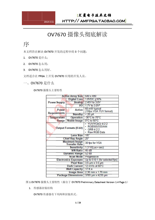
OV7670 摄像头模块介绍OV7670 摄像头模块简介OV7670是OV(OmniVision)公司生产的一颗1/6寸的CMOS VGA 图像传感器。
该传感器体积小、工作电压低,提供单片VGA摄像头和影像处理器的所有功能。
通过SCCB 总线控制,可以输出整帧、子采样、取窗口等方式的各种分辨率8位影像数据。
该产品VGA图像最高达到30帧/秒。
用户可以完全控制图像质量、数据格式和传输方式。
所有图像处理功能过程包括伽玛曲线、白平衡、度、色度等都可以通过SCCB接口编程。
OmmiVision 图像传感器应用独有的传感器技术,通过减少或消除光学或电子缺陷如固定图案噪声、托尾、浮散等,提高图像质量,得到清晰的稳定的彩色图像。
OV7670 摄像头模块特点1、高灵敏度、低电压适合嵌入式应用。
2、标准的SCCB接口,兼容IIC接口。
3、支持RawRGB、RGB(GBR4:2:2,RGB565/RGB555/RGB444),YUV(4:2:2)和YCbCr(4:2:2)输出格式。
4、支持VGA、CIF,和从CIF到40*30的各种尺寸输出。
5、支持自动曝光控制、自动增益控制、自动白平衡、自动消除灯光条纹、自动黑电平校准等自动控制功能。
同时支持色饱和度、色相、伽马、锐度等设置。
6、支持闪光灯。
7、支持图像缩放。
OV7670 摄像头模块功能框图OV7670传感器包括如下一些功能模块。
1、感光整列(Image Array)OV7670总共有656*488个像素,其中640*480个有效(即有效像素为30W)。
2、时序发生器(Video Timing Generator)时序发生器具有的功能包括:整列控制和帧率发生(7种不同格式输出)、内部信号发生器和分布、帧率时序、自动曝光控制、输出外部时序(VSYNC、HREF/HSYNC和PCLK)。
3、模拟信号处理(Analog Processing)模拟信号处理所有模拟功能,并包括:自动增益(AGC)和自动白平衡(AWB)。
微雪电子OV7670 Camera Board(B) 使用手册

OV7670 Camera Board (B)使 用 说 明 V1.2微雪电子w ww.w a v e s目录1.OV7670一般摄像头模块1.1简介1.2管脚定义1.3控制方式说明 1.4采集图像的基本方法2.OV7670带FIFO 摄像头模块2.1简介 2.2管脚定义2.3控制方式说明 2.4图像采集的基本方法3.问题解答3.1图像采集难吗3.2学习图像方面的知识需要哪些基础 3.3初学者遇到问题该怎么解决 3.4模块提供那些资料3.5单片机能够真正的采集图像吗3.6带FIFO 和不带FIFO 的模块到底哪个好,有什么区别 3.7模块上有晶振好,还是没晶振好 3.8摄像头寄存器该怎么设置3.9 微雪电子模块提供的Demo 输出的数据是什么格式的w ww.w a ve s3.10如果想真正实现图像的采集并且能够处理图像数据该如何做 3.11 微雪电子的那个模块能够适合飞思卡尔小车的比赛 3.12 微雪电子的模块输出到底是模拟的还是数字的3.13 微雪电子模块的质量如何3.14 微雪电子几种驱动板的功能,区别是什么 3.15如何检测微雪电子摄像头模块是否损坏 3.16 微雪电子摄像头模块和模组的区别是什么w ww.w a ve s1.OV7670一般摄像头模块1.简介:OV7670一般模块指微雪电子推出的低成本数字输出CMOS 摄像头,其摄像头包含30w 像素的CMOS 图像感光芯片,3.6mm 焦距的镜头和镜头座,板载CMOS 芯片所需要的各种不同电源(电源要求详见芯片的数据文件),板子同时引出控制管脚和数据管脚,方便操作和使用。
图1.OV7670一般模块2.管脚定义:如图,控制传感器所需的管脚定义如下:3V3-----输入电源电压(推荐使用3.3,5V 也可,但不推荐使用) GDN-----接地点SIO_C---SCCB 接口的控制时钟(注意:部分低级单片机需要上拉控制,和I2C 接口类似)w ww.w a ve sSIO_D---SCCB 接口的串行数据输入(出)端(注意:部分低级单片机需要上拉控制,和I2C 接口类似)VSYNC---帧同步信号(输出信号) HREF----行同步信号(输出信号)PCLK----像素时钟(输出信号) XCLCK---时钟信号(输入信号) D0-D7---数据端口(输出信号) RESTE---复位端口(正常使用拉高)PWDN----功耗选择模式(正常使用拉低)图2.微雪摄像头接口定义3.控制方式说明采集图像数据需要严格按照OV 公司的芯片时序进行,这些时序包括:(1) S CCB 通讯时序,其作用是设置芯片内部寄存器,以控制图像的各种所w ww.w a ve s需功能。
OV7670摄像头彻底解读
4 / 23
2013‐2‐21
[艾曼电子技术文档 HTTP:// ]
二、 OV7670 摄像头怎么用
1. 摄像头硬件电路
数据传输的终止
图 8 SCCB 终止信号 tPSC 是 SCCB——E 上升沿,SIO_D 保持逻辑高电平的时间,最小为 15ns; tPSA 是 SIO_D 上升沿,SCCB_E 必须保持低电平的时间,最小为 0ns。
2.3 SCCB 写时序
写时序由 3 相构成。先写设备地址,再写寄存器地址,最后写寄存器的值,即 ID‐Address + SUB‐Address + W‐Data。OV7670 的设备地址为 0x42,最后一位用来判断读写,即读的时候为 0x43。
2 / 23
2013‐2‐21
[艾曼电子技术文档 HTTP:// ]
15
DVDD
Power
Power supply (VDD-C= 1.8 VDC + 10%) for digital output drive
16
HREF
Output
HREF output
Power Down Mode Selection - active high, internal
U1
A1 A2 A3 A4 A5 B1 B2 B3 B4 B5 C1 C2 D1 D2 E1 E2 E3 E4 E5 F1 F2 F3 F4 F5
AVDD SIO_D SIO_C D1 D3 PWDN VREF2 AGND D0 D2 DVDD VREF1 VSYNC HREF PCLK STROBE XCLK D7 D5 DOVDD RESET# DOGND D6 D4
基于FPGA的OV7670摄像头和液晶显示产品简介
基于FPGA的OV7670摄像头和液晶显示产品简介
一、总体介绍
该产品以ALTERA公司Cyclone II系列FPGA的EP2C8Q208C8N芯片为主控核心,通过在FPGA 外围扩展1片SDRAM、1片SRAM、1片Nor FLASH、1个SD卡座、一个OV7670摄像头模块、一块2.8寸TFT液晶显示屏等外围设备构成的图像采集、分析和存储系统。
在此硬件基础上,产品配套有以上外设的Verilog HDL或者NIOSII的驱动程序。
用户可以在此基础上开发设计基于FPGA硬件编码或者NIOSII的图像处理程序。
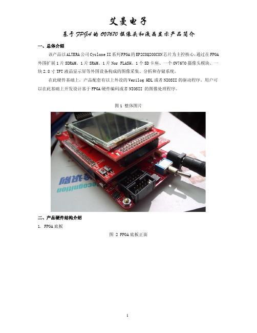
图1整体图片
二、产品硬件结构介绍
1.FPGA底板
图2FPGA底板正面
图2中,1为K4S641632,64M bit,2为EP2C8Q208C8N FPGA芯片,3为IS61LV25616A-10TI 512Kbyte的SRAM芯片,4为AM29LV320DB32Mbit芯片。
5为FPGA的AS模式编程接口,6为FPGA的JTAG模式编程接口。
图3FPGA底板反面
钟。
2.中间层扩展板
该板主要起转接作用,板子下面跟FPGA底板连接,上面跟液晶扩展板和摄像头模块连接。
3.液晶扩展板
该板带一块2.8寸TFT触摸液晶屏,带触摸屏AD转换芯片。
OV7670照相模组硬件应用指南1.01 OVT
O
V
Co
修改日期:2007-12-12 版本: 1.06
nf
OmniVision 公司机密
id e
nt
ia l
OV7670 照相模组硬件应用指南
Table of Contents
1. OV7670 模组参考设计................................................................................................................... 3 注:...................................................................................................................................................... 3 1.PWDN 和 RESET 不用时,应接地.................................................................................................3 2. OV7670 模组接口参考设计........................................................................................................... 4 2.1 引脚定义...............................................................................................................................
OV7670及其在3G流媒体服务中的应用
OV7670及其在3G流媒体服务中的应用魏崇毓;韩永亮【摘要】在3G网络视频监控迅速崛起的时代背景下,介绍一种CMOS图像传感器OV7670.从其基本结构、编程功能及数字图像的输出方面做了具体研究,最后给出一种OV7670在3G流媒体(视频流)服务中的应用方案,对3G无线视频传输系统设计具有指导意义.【期刊名称】《现代电子技术》【年(卷),期】2010(033)023【总页数】3页(P74-76)【关键词】传感器;OV7670;YUV 4∶2∶2;PXA310;视频传输【作者】魏崇毓;韩永亮【作者单位】青岛科技大学,信息科学技术学院,山东,青岛,266061;青岛科技大学,信息科学技术学院,山东,青岛,266061【正文语种】中文【中图分类】TN919-340 引言随着3G时代的到来及其迅猛的发展,3G手机视频监控成为一个最热门的话题,有关这一方面的研究也越来越多[1]。
所有的无线视频传输都离不开一个视频数据量的问题,即视频传输既要满足终端图像信息的清晰度,又要考虑低带宽条件限制下数据率问题,本文介绍了一种CMOS图像传感器芯片OV7670,适用于上述特定条件下的3G无线视频监控系统。
1 OV7670的基本结构OV7670是美国Omnivision公司开发的CMOS彩色图像传感器芯片,其VGA 图像最高达到30帧/s,用户可以完全控制图像质量、数据格式和传输方式,通过SCCB总线控制,可以输出整帧、子采样、取窗口等方式的各种分辨率的8位图像数据,并且所有图像处理功能包括白平衡、饱和度、色度等都可以通过SCCB接口编程,加上Omnivision图像传感器拥有独特的传感器技术,通过减少或消除光学或电子缺陷(如固定图案噪声、拖尾、浮散等),可以提高图像质量,得到清晰稳定的彩色图像[2]。
其性能特点有:(1) 标准的SCCB接口,兼容I2C接口。
(2) 支持VGA,CIF,以及从40×30到CIF的各种分辨率。
ov7670寄存器配置调试总结
废话后面说,先直接上OV7670寄存器的配置部分const uint8_t OV7670_Reg[][2]={//Frame Rate Adjustment for 24Mhz input clock//30fps PCLK=24MHz{0x11, 0x80},//软件应用手册上设置的是0x80,例程设置的是0x00{0x6b, 0x0a},//PLL控制,软件应用手册上设置的是0x0a,例程设置的是0x40,将PLL调高的话就会产生花屏{0x2a, 0x00},{0x2b, 0x00},{0x92, 0x00},{0x93, 0x00},{0x3b, 0x0a},//Output format{0x12, 0x14},//QVGA(320*240)、RGB//RGB555/565 option(must set COM7[2] = 1 and COM7[0] = 0){0x40, 0x10},//RGB565,effective only when RGB444[1] is low{0x8c, 0x00},//Special effects - 特效//normal{0x3a, 0x04},{0x67, 0xc0},{0x68, 0x80},//Mirror/VFlip Enable - 水平镜像/竖直翻转使能{0x1e, 0x37},//修改配置值将产生图像显示上下或左右颠倒//Banding Filter Setting for 24Mhz Input Clock - 条纹滤波器//30fps for 60Hz light frequency//{0x13, 0xe7},//banding filer enable//{0x9d, 0x98},//50Hz banding filer//{0x9e, 0x7f},//60Hz banding filer//{0xa5, 0x02},//3 step for 50Hz//{0xab, 0x03},//4 step for 60Hz//{0x3b, 0x02},//select 60Hz banding filer//Simple White Balance - 白平衡//{0x13, 0xe7},//AWB、AGC、AGC Enable and ...//{0x6f, 0x9f},//simple AWB//AWBC - 自动白平衡控制(Automatic white balance control)//{0x43, 0x14},//用户手册里这些寄存器的值都是保留(Reserved),不用设置的呀?//{0x44, 0xf0},//{0x45, 0x34},//{0x46, 0x58},//{0x47, 0x28},//{0x48, 0x3a},//AWB Control//{0x59, 0x88},//用户手册连寄存器都是保留,初始值都没提供//{0x5a, 0x88},//{0x5b, 0x44},//{0x5c, 0x67},//{0x5d, 0x49},//{0x5e, 0x0e},//AWB Control//{0x6c, 0x0a},//{0x6d, 0x55},//{0x6e, 0x11},//{0x6f, 0x9f},//AGC/AEC - Automatic Gain Control自动增益补偿/Automatic exposure Control自动曝光控制//{0x00, 0x00},//{0x14, 0x20},//{0x24, 0x75},//{0x25, 0x63},//{0x26, 0xA5},//AEC algorithm selection - AEC公式选择//{0xaa, 0x94},//基于平均值的AEC算法Average-based AEC algorithm/基于直方图的AEC算法Histogram-based AEC algorithm//基于直方图的AGC/AEC的控制//{0x9f, 0x78},//{0xa0, 0x68},//{0xa6, 0xdf},//{0xa7, 0xdf},//{0xa8, 0xf0},//{0xa9, 0x90},//Fix Gain Control - 固定增益控制//{0x69, 0x5d},//Fix gain for Gr channel/for Gb channel/for R channel/for B channel//Color saturation 颜色饱和度+ 0//{0x4f, 0x80},//{0x50, 0x80},//{0x51, 0x00},//{0x52, 0x22},//{0x53, 0x5e},//{0x54, 0x80},//{0x58, 0x9e},//Brightness - 亮度+ 0//{0x55, 0x00},//Contrast - 对比度+ 0//{0x56, 0x40},//Gamma Curve - 伽马曲线//{0x7a, 0x20},//{0x7b, 0x1c},//{0x7c, 0x28},//{0x7d, 0x3c},//{0x7e, 0x55},//{0x7f, 0x68},//{0x80, 0x76},//{0x81, 0x80},//{0x82, 0x88},//{0x83, 0x8f},//{0x84, 0x96},//{0x85, 0xa3},//{0x86, 0xaf},//{0x87, 0xc4},//{0x88, 0xd7},//{0x89, 0xe8},//Matrix Coefficient - 色彩矩阵系数//{0x4f, 0x80},//{0x50, 0x80},//{0x51, 0x00},//{0x52, 0x22},//{0x53, 0x5e},//{0x54, 0x80},//Lens Correction Option - 镜头补偿选项 //{0x62, 0x00},//{0x63, 0x00},//{0x64, 0x04},//{0x65, 0x20},//{0x66, 0x05},//{0x94, 0x04},//effective only when LCC5[2] is high//{0x95, 0x08},//effective only when LCC5[2] is high//注释这些配置的话,就倾斜显示,并显示多块,这到底是控制什么的?跟时序图有关?{0x17, 0x16},//行频Horizontal Frame开始高八位(低三位在HREF[2:0]){0x18, 0x04},//行频Horizontal Frame结束高八位(低三位在HREF[5:3]){0x19, 0x02},//场频Vertical Frame开始高八位(低二位在VREF[1:0]){0x1a, 0x7b},//场频Vertical Frame结束高八位(低二位在VREF[3:2]){0x32, 0x80},//HREF{0x03, 0x06},//VREF//注释这个配置的话,就显示花屏了{0x15, 0x02},//配置PCLK、HREF、VSYNC相关//Automatic black Level Compensation - 自动黑电平校正{0xb0, 0x84},//调试时注释这项配置时,颜色显示不正常了,红色练绿色,绿色变红色,但用户手册对这寄存器是保留RSVD//{0xb1, 0x0c},//{0xb2, 0x0e},//{0xb3, 0x82},//{0xb8, 0x0a},//SCALING_xx寄存器//{0x70, 0x00},//{0x71, 0x00},//{0x72, 0x11},//{0x73, 0x08},//{0x3e, 0x00},//ADC//{0x37, 0x1d},//ADC控制ADC Control//{0x38, 0x71},//ADC和模拟共模控制ADC and Analog Common Mode Control//{0x39, 0x2a},//ADC偏移控制ADC Offset Control//零杂的寄存器//{0x92, 0x00},//空行低八位Dummy Line low 8 bits//{0xa2, 0x02},//像素时钟延时//{0x0c, 0x0c},//{0x10, 0x00},//{0x0d, 0x01},//{0x0f, 0x4b},//{0x3c, 0x78},//{0x74, 0x19},//用户手册里这几个寄存器都是保留RSVD//{0x0e, 0x61},//{0x16, 0x02},//{0x21, 0x02},//{0x22, 0x91},//{0x29, 0x07},//{0x33, 0x0b},//{0x35, 0x0b},//{0x4d, 0x40},//{0x4e, 0x20},//{0x8d, 0x4f},//{0x8e, 0x00},//{0x8f, 0x00},//{0x90, 0x00},//{0x91, 0x00},//{0x96, 0x00},//{0x9a, 0x80},};刚开始学OV7670摄像头,我想大家跟我一样心里很毛躁吧,一个模块需要你配置100多个寄存器,但用户手册对寄存器的介绍却草草的一笔带过,自己无从下手啊,只能看开发板给的例程和上网找一些大虾的帖子了。
ov7670寄放器配置调试总结
废话后面说,先直接上OV7670寄放器的配置部份const uint8_t OV7670_Reg[][2]={//Frame Rate Adjustment for 24Mhz input clock//30fps PCLK=24MHz{0x11, 0x80},//软件应用手册上设置的是0x80,例程设置的是0x00{0x6b, 0x0a},//PLL操纵,软件应用手册上设置的是0x0a,例程设置的是0x40,将PLL调高的话就会产生花屏{0x2a, 0x00},{0x2b, 0x00},{0x92, 0x00},{0x93, 0x00},{0x3b, 0x0a},//Output format{0x12, 0x14},//QVGA(320*240)、RGB//RGB555/565 option(must set COM7[2] = 1 and COM7[0] = 0){0x40, 0x10},//RGB565,effective only when RGB444[1] is low{0x8c, 0x00},//Special effects - 特效//normal{0x3a, 0x04},{0x67, 0xc0},{0x68, 0x80},//Mirror/VFlip Enable - 水平镜像/竖直翻转使能{0x1e, 0x37},//修改配置值将产生图像显示上下或左右倒置//Banding Filter Setting for 24Mhz Input Clock - 条纹滤波器//30fps for 60Hz light frequency//{0x13, 0xe7},//banding filer enable//{0x9d, 0x98},//50Hz banding filer//{0x9e, 0x7f},//60Hz banding filer//{0xa5, 0x02},//3 step for 50Hz//{0xab, 0x03},//4 step for 60Hz//{0x3b, 0x02},//select 60Hz banding filer//Simple White Balance - 白平稳//{0x13, 0xe7},//AWB、AGC、AGC Enable and ...//{0x6f, 0x9f},//simple AWB//AWBC - 自动白平稳操纵(Automatic white balance control)//{0x43, 0x14},//用户手册里这些寄放器的值都是保留(Reserved),不用设置的呀? //{0x44, 0xf0},//{0x45, 0x34},//{0x46, 0x58},//{0x47, 0x28},//{0x48, 0x3a},//AWB Control//{0x59, 0x88},//用户手册连寄放器都是保留,初始值都没提供//{0x5a, 0x88},//{0x5b, 0x44},//{0x5c, 0x67},//{0x5d, 0x49},//{0x5e, 0x0e},//AWB Control//{0x6c, 0x0a},//{0x6d, 0x55},//{0x6e, 0x11},//{0x6f, 0x9f},//AGC/AEC - Automatic Gain Control自动增益补偿/Automatic exposure Control自动曝光操纵//{0x00, 0x00},//{0x14, 0x20},//{0x24, 0x75},//{0x25, 0x63},//{0x26, 0xA5},//AEC algorithm selection - AEC公式选择//{0xaa, 0x94},//基于平均值的AEC算法Average-based AEC algorithm/基于直方图的AEC算法Histogram-based AEC algorithm//基于直方图的AGC/AEC的操纵//{0x9f, 0x78},//{0xa0, 0x68},//{0xa6, 0xdf},//{0xa7, 0xdf},//{0xa8, 0xf0},//{0xa9, 0x90},//Fix Gain Control - 固定增益操纵//{0x69, 0x5d},//Fix gain for Gr channel/for Gb channel/for R channel/for B channel//Color saturation 颜色饱和度+ 0 //{0x4f, 0x80},//{0x50, 0x80},//{0x51, 0x00},//{0x52, 0x22},//{0x53, 0x5e},//{0x54, 0x80},//{0x58, 0x9e},//Brightness - 亮度+ 0//{0x55, 0x00},//Contrast - 对照度+ 0//{0x56, 0x40},//Gamma Curve - 伽马曲线//{0x7a, 0x20},//{0x7b, 0x1c},//{0x7c, 0x28},//{0x7d, 0x3c},//{0x7e, 0x55},//{0x7f, 0x68},//{0x80, 0x76},//{0x81, 0x80},//{0x82, 0x88},//{0x83, 0x8f},//{0x84, 0x96},//{0x85, 0xa3},//{0x86, 0xaf},//{0x87, 0xc4},//{0x88, 0xd7},//{0x89, 0xe8},//Matrix Coefficient - 色彩矩阵系数//{0x4f, 0x80},//{0x50, 0x80},//{0x51, 0x00},//{0x52, 0x22},//{0x53, 0x5e},//{0x54, 0x80},//Lens Correction Option - 镜头补偿选项//{0x62, 0x00},//{0x63, 0x00},//{0x64, 0x04},//{0x65, 0x20},//{0x66, 0x05},//{0x94, 0x04},//effective only when LCC5[2] is high//{0x95, 0x08},//effective only when LCC5[2] is high//注释这些配置的话,就倾斜显示,并显示多块,这究竟是操纵什么的?跟时序图有关? {0x17, 0x16},//行频Horizontal Frame开始高八位(低三位在HREF[2:0]){0x18, 0x04},//行频Horizontal Frame终止高八位(低三位在HREF[5:3]){0x19, 0x02},//场频Vertical Frame开始高八位(低二位在VREF[1:0]){0x1a, 0x7b},//场频Vertical Frame终止高八位(低二位在VREF[3:2]){0x32, 0x80},//HREF{0x03, 0x06},//VREF//注释那个配置的话,就显示花屏了{0x15, 0x02},//配置PCLK、HREF、VSYNC相关//Automatic black Level Compensation - 自动黑电平校正{0xb0, 0x84},//调试时注释这项配置时,颜色显示不正常了,红色练绿色,绿色变红色,但用户手册对这寄放器是保留RSVD//{0xb1, 0x0c},//{0xb2, 0x0e},//{0xb3, 0x82},//{0xb8, 0x0a},//SCALING_xx寄放器//{0x70, 0x00},//{0x71, 0x00},//{0x72, 0x11},//{0x73, 0x08},//{0x3e, 0x00},//ADC//{0x37, 0x1d},//ADC操纵ADC Control//{0x38, 0x71},//ADC和模拟共模操纵ADC and Analog Common Mode Control//{0x39, 0x2a},//ADC偏移操纵ADC Offset Control//零杂的寄放器//{0x92, 0x00},//空行低八位Dummy Line low 8 bits//{0xa2, 0x02},//像素时钟延时//{0x0c, 0x0c},//{0x10, 0x00},//{0x0d, 0x01},//{0x0f, 0x4b},//{0x3c, 0x78},//{0x74, 0x19},//用户手册里这几个寄放器都是保留RSVD//{0x0e, 0x61},//{0x16, 0x02},//{0x21, 0x02},//{0x22, 0x91},//{0x29, 0x07},//{0x33, 0x0b},//{0x35, 0x0b},//{0x4d, 0x40},//{0x4e, 0x20},//{0x8d, 0x4f},//{0x8e, 0x00},//{0x8f, 0x00},//{0x90, 0x00},//{0x91, 0x00},//{0x96, 0x00},//{0x9a, 0x80},};刚开始学OV7670摄像头,我想大伙儿跟我一样内心很毛躁吧,一个模块需要你配置100多个寄放器,但用户手册对寄放器的介绍却草草的一笔带过,自己无从下手啊,只能看开发板给的例程和上网找一些大虾的帖子了。
- 1、下载文档前请自行甄别文档内容的完整性,平台不提供额外的编辑、内容补充、找答案等附加服务。
- 2、"仅部分预览"的文档,不可在线预览部分如存在完整性等问题,可反馈申请退款(可完整预览的文档不适用该条件!)。
- 3、如文档侵犯您的权益,请联系客服反馈,我们会尽快为您处理(人工客服工作时间:9:00-18:30)。
OV7670 Dual Camera Module Application NotesLast Modified: April 2nd, 2007Document Revision: 1.00OmniVision Technologies, Inc. reserves the right to make changes without further notice to any product herein to improve reliability, function or design. OmniVision does not assume any liability arising out of the application or use of any project, circuit described herein; neither does it convey any license under its patent nor the right of others.This document contains information of a proprietary nature. None of this information shall be divulged to persons other than OmniVision Technologies, Inc. employee authorized by the nature of their duties to receive such information,or individuals or organizations authorized by OmniVision Technologies, Inc.Table of Contents1. OV7670 Dual Camera Solution (3)1.1 OV7670 Dual Camera Design with 2 Connectors (3)1.1.1 Camera Module Reference design (3)1.1.2 Camera phone Reference Design (4)1.2 OV7670 Dual Camera Design with Single Connector (5)1.2.1 Camera Module Reference design (5)1.2.2 Camera Phone Reference Design (6)2 OV7670 Dual Camera Operation (7)2.1 Power Saving Modes (7)2.2 Dual Camera Operation in Power Down Mode (7)2.2.1 Battery On (7)2.2.2 Enter Camera 1 (8)2.2.3 Exit Camera 1 (8)2.2.4 Enter Camera 2 (9)2.2.5 Exit Camera 2 (9)2.3 Dual Camera Operation in Power Off Mode (9)2.3.1 Battery On (9)2.3.2 Enter Camera 1 (10)2.3.3 Exit Camera 1 (11)2.3.4 Enter Camera 2 (11)2.3.5 Exit Camera 2 (12)3. SCCB Bus sharing (13)4. Timing Considerations for Phone PCB Design (13)4.1 Sample with PCLK (14)4.2 Sample with XCLK (14)4.3 Using EMI/ESD Device (15)5. Camera Module Testing (15)5.1 Test Board Modification (15)5.2 Test Procedure (16)5.2.1 Test Camera 1 (16)5.2.2 Test Camera 2 (16)1. OV7670 Dual Camera SolutionDual OV7670 cameras could be used to share single camera port. The PWDN pins of the 2 cameras should be controlled separately by GPIO. The PWDN1 and PWDN2 selects which camera is working and which camera is power down. The outputs (data bus, clock and sync signals) of power down camera could be set to tri-state. So that the outputs of 2 cameras could share same bus.If dual OV7670 cameras are used in camera phone design, please pay attention to following items.a. DVDD should be supplied by external power supply. If DVDD is not supplied by external, OV7670 may not be able to initialize correctly by SCCB initialization.b. PWDN of the two cameras should be controlled separately. PWDN signals are used to select which camera is working and which camera is standby.c. If power off mode is used, the powers of dual cameras should be turned on/turn off simultaneously. If one camera is power on, the other camera is power off, there would be a big current leakage and the power on camera can not work correctly.1.1 OV7670 Dual Camera Design with 2 ConnectorsEach camera has separate connector. In this case, the camera module design is same as single camera solution.1.1.1 Camera Module Reference designNote:AVDD is 2.45V to 2.8V sensor analog power.DVDD is 1.8V sensor digital power.DOVDD is 2.5V to 3.3V sensor digital IO power.Sensor AGND and DGND should be separated and connect to a single point at outside PCB (Don't connect inside module).C1 should close to sensor VREF and AGND.C2 should close to sensor AVDD and AGND.D7:D0 is module YUV and RGB 8bits output.1.1.2 Camera phone Reference DesignIf DOVDD uses different power supply than AVDD, then 3 regulators should be used.If DOVDD uses the same voltage as AVDD, then only 2 regulators are required. R/C filter is used to separate AVDD from DOVDD.Please note thata. The AGND and DGND should be separate inside module and connected together on phone PCB very close to camera module connector.b. Strobe (LED) of the 2 cameras should be separated. The strobe LED should face same direction as the driven camera.c. RESET# pin of camera modules should be controlled by GPIO. It should not be connected to DOVDD as single camera application.1.2 OV7670 Dual Camera Design with Single ConnectorDual cameras share the same FPC and connector. In this case, the camera module design is different than singe camera application.1.2.1 Camera Module Reference designThe PWDN and STRB of the 2 sensors are separated. Other pins such as XCLK, RESET#, SIO_C, SIO_D, D[7:0], PCLK, HREF, VSYNC are connected together to share the same bus.1.2.2 Camera Phone Reference DesignCam era_OnIf DOVDD uses different power supply than AVDD then 3 regulators should be used.Cam era_OnIf DOVDD uses the same voltage as AVDD, then only 2 regulators are required.Note:a. The AGND and DGND should be separate inside module and connected together on phone PCBvery close to camera module connector.b. Strobe (LED) of the 2 cameras should be separated. The strobe LED should face same direction as the driven camera.c. RESET# pin of camera modules should be controlled by GPIO. It should not be connected to DOVDD as single camera application.2 OV7670 Dual Camera Operation2.1 Power Saving ModesThere are 2 kind of power saving modes: power down mode and power off mode. Power down mode means that in power saving mode, all the power supplies to dual camera module are kept. The cameras are set into power down mode by pull high PWDN1 and PWDN2. Power off mode means that in power saving mode, all the power supplies to dual camera module are cut.2.2 Dual Camera Operation in Power Down Mode2.2.1 Battery OnT1: from powers on to PWDN2 pull high, >= 3mst2: from PWDN1 pull high to RESET# pull high, >= 3mst3: from RESET# pull high to SCCB initialization, >= 10mst4: from PWDN1 pull high to PWDN2 pull low, >= 100mst5: from PWDN2 pull low to SCCB initialization, >= 10msStep 1:Reset# is applied to reset both cameras.ResetPDWN1PDWN2SIO_CSIO_DDOVDDDVDDAVDDXCLKStep 2:DOVDD, DVDD and AVDD powers are applied. The 3 powers could be applied simultaneously. If applied separately, the power on sequence should be DOVDD first, DVDD second and AVDD last.Step 3:after 3ms of last power applied, pull high PWDN2. Set camera 2 to power down mode.Step 4:After 3ms, Pull RESET# high.Step 5:After 10ms, initialize camera 1 by SCCB initialization.Step 6:Pull high PWDN1. Set camera 1 to power down mode.Step 7:after 100ms, pull low PWDN2. Set camera 2 to working mode.Step 8:after 10ms, initialize camera 2 by SCCB initialization.Step 9:Pull PWDN2 to high. Both camera are in power down mode.The XCLK should be set to low when both cameras are power down to minimize standby current.2.2.2 Enter Camera 1Step 1:Pull high PWDN2. Pull Low PWDN1. Apply XCLK.Step 2:After 10ms, initialize camera 1 by SCCB initialization.2.2.3 Exit Camera 1Step 1:Pull High PWDN1Step 2:after 100ms, pull low XCLK2.2.4 Enter Camera 2Step 1:Pull high PWDN1, Pull low PWDN2. Apply XCLKStep 2:After 10ms, initialize camera 2 by SCCB initialization.2.2.5 Exit Camera 2Step 1:Pull High PWDN2.Step 2:After 100ms, pull low XCLK.2.3 Dual Camera Operation in Power Off Mode2.3.1 Battery OnNo operation. Both cameras are power off.PWDN1PWDN2SIO_C SIO_DXCLKPWDN1PWDN2SIO_CSIO_DXCLK2.3.2 Enter Camera 1Step 1:Reset# is applied to reset both cameras.Step 2:DOVDD, DVDD and AVDD powers are applied. The 3 powers could be applied simultaneously. If applied separately, the power on sequence should be DOVDD first, DVDD second and AVDD last.Step 3:after 3ms of last power applied, pull high PWDN1. Set camera 1 to power down mode.Step 4:After 3ms, Pull RESET# high.Step 5:After 10ms, initialize camera 2 by SCCB initialization.Step 6:Pull high PWDN2. Set camera 2 to power down mode.Step 7:after 100ms, pull low PWDN1. Set camera 1 to working mode.Step 8:after 10ms, initialize camera 1 by SCCB initialization.ResetPDWN2PDWN1SIO_CSIO_DDOVDDDVDDAVDDXCLKT1: from powers on to PWDN1 pull high, >= 3mst2: from PWDN1 pull high to RESET# pull high, >= 3ms t3: from RESET# pull high to SCCB initialization, >= 10ms t4: from PWDN2 pull high to PWDN1 pull low, >= 100ms t5: from PWDN1 pull low to SCCB initialization, >= 10ms2.3.3 Exit Camera 1Step 1.Pull low XCLK,Step 2.Turn off AVDD, DVDD and DOVDD. The 3 powers could be turned off simultaneously. If turned off separately, AVDD should be turned off first, DVDD second and DOVDD third.Step 3.Pull Low PWDN1, PWDN2 and RESET#2.3.4 Enter Camera 2Step 1:Reset# is applied to reset both cameras.Step 2:DOVDD, DVDD and AVDD powers are applied. The 3 powers could be applied simultaneously. If applied separately, the power on sequence should be DOVDD first, DVDD second and AVDD last.Step 3:after 3ms of last power applied, pull high PWDN2. Set camera 2 to power down mode.Step 4:After 3ms, Pull RESET# high.DOVDDDVDDAVDDXCLK Reset PWDN1PWDN2Step 5:After 10ms, initialize camera 1 by SCCB initialization.Step 6:Pull high PWDN1. Set camera 1 to power down mode.Step 7:after 100ms, pull low PWDN2. Set camera 2 to working mode.Step 8:after 10ms, initialize camera 2 by SCCB initialization.T1:from powers on to PWDN2 pull high, >= 3mst2: from PWDN1 pull high to RESET# pull high, >= 3ms t3: from RESET# pull high to SCCB initialization, >= 10ms t4: from PWDN1 pull high to PWDN2 pull low, >= 100ms t5: from PWDN2 pull low to SCCB initialization, >= 10ms2.3.5 Exit Camera 2Step 1.Pull low XCLK,Step 2.Turn off AVDD, DVDD and DOVDD. The 3 powers could be turned off simultaneously. If turned off separately, AVDD should be turned off first, DVDD second and DOVDD third.Step 3.Reset PDWN1PDWN2SIO_C SIO_D DOVDD DVDDAVDDXCLKPull Low PWDN1, PWDN2 and RESET#3. SCCB Bus sharingThe SCCB bus of OV7670 dual camera solution could share with other I2C device. WhenOV7670 is working, the read/write operation is separated by device address. The device address of OV7670 is 0x42. I2C read/write to address other than the 2 address above will not affect SCCB registers of OV7670.It is recommended to use power down mode when SCCB bus is shared with other device. When OV7670 dual camera module is power down, the SCCB Bus is leave free. The power down of OV7670 doesn't affect the read/write of other I2C device as long as the DVDD of OV7670 is provided by external regulator.It is not recommended to use power off mode when SCCB bus is shared with other device. When OV7670 dual camera module is power off, all the inputs to OV7670 should be pulled low. The inputs include XCLK, RESET#, PWDN1 and PWDN2. If any if the input is not pulled low, the input would leak current to DVDD/DOVDD of OV7670, then the SIO_D and SIO_C may be pulled to unknown state and caused I2C malfunction.4. Timing Considerations for Phone PCB DesignThere are 2 clock signal for OV7670 dual camera module. One is the main clock (input clock) XCLK, the other is the pixel clock (output clock) PCLK. Some backend/baseband chips may use XCLK as pixel sample clock, some backend/baseband chips may use PCLK as pixel sample clock. It is recommended to use PCLK as pixel sample clock.DOVDDDVDDAVDDXCLK Reset#PWDN2PWDN1Let's look at the clock distribution first.So the delay of video data to clock at backend/baseband side is very critical for timing design. If the delay is over the spec. of backend/baseband chip, the backend/baseband chip can not get video data correctly. The incorrect video data may have wrong color, fixed or moving horizontal lines.From the clock distribution diagram above, the delays are:Delay_XCLK = 0Delay_PCLK = PCB_Delay_XCLK + Internal_Delay + PLL_Delay + PCB_Delay_PCLKDelay_Data = PCB_Delay_XCLK + Internal_Delay + PLL_Delay + PCLK_to_Data_Delay + PCB_Delay_Data4.1 Sample with PCLKIf Backend/baseband sample video data with PCLK, the clock data delay isclock_data_delay = Delay_Data – Delay_PCLK= PCLK_to_Data_Delay + PCB_Delay_Data – PCB_Delay_PCLK The clock data delay is not related with PCB delay of XCLK.If PCB is carefully designed so that the wire length of PCLK and Data are same, thenPCB_Delay_Data = PCB_Delay_PCLK, the clock data delay isclock_data_delay = PCLK_to_Data_Delay, not related to PCB layout4.2 Sample with XCLKIf Backend/baseband sample video data with PCLK, the clock data delay isclock_data_delay = Delay_Data – Delay_XCLK= PCB_Delay_XCLK + Internal_Delay + PLL_Delay + PCLK_to_Data_Delay + PCB_Delay_Data The data to clock delay at Baseband/Backend chip are much bigger than sampled with PCLK. And the delay is highly depend on PCB layout. So if XCLK is used to sample video data, it is very likely to have timing issue which would cause incorrect video data.4.3 Using EMI/ESD DeviceIf EMI/ESD device are used in phone design, the PCB delay increase very much. It should be very careful to manipulate the delays to meet timing spec. of backend/baseband chips.1.Try to use PCLK as sample clock of video data.2.XCLK and PCLK should not share ESD/EMI device with other signals. Use dedicateESD/EMI device or R/C filters for XCLK and PCLK. So that the delay on XCLK andPCLK could be adjusted later.3.For dual camera module, use single ESD/EMI device or single R?C filter for XCLK andPCLK to minimize clock delay.4.Carefully layout PCB to keep XCLK wire as short as possible, PCLK wire the same lengthas data lines.5.Minimize the length of FPC of camera module.5. Camera Module TestingIf the dual cameras have separate connector, then usual camera module test procedure forOV7670 could be applied. There is no need to do any change neither on USB 2.0 test board nor camera module testing method.If the dual cameras share same connector, then the USB 2.0 test board should be modified and the testing method should be changed.5.1 Test Board ModificationTo test dual cameras share same connector, the USB 2.0 test board should be modified.Even there are 2 cameras on same FPC, there is only one camera work at the same time. PWDN pins are used to select which camera is work and which camera is power down.It is recommended to use the PWDN control circuit above. It eliminate the possibility that 2 cameras are both set to working mode which may damage the cameras. SW1 is used to select camera. SW2 is used to set both camera to power down mode.SW1SW2Camera SelectionL L Camera 1 power down, camera 2 workingH L Camera 1 working, camera 2 power downAny H Both camera power down5.2 Test Procedure5.2.1 Test Camera 1Un-plug USB 2.0 test board. Insert camera module into connector. Adjust the switches to pull PWDN1 of camera 1 to Low and PWDN2 of Camera 2 to high.Plug in USB 2.0 test board. The camera 2 is in power down mode. The Camera 1 is in active mode. The camera driver initialize OV7670 camera 1. After the LED is on, the camera 1 is ready. Amcap or other application could be opened to test OV7670 camera 1.5.2.2 Test Camera 2Un-plug USB 2.0 test board. Insert camera module into connector. Adjust the switches to pull PWDN1 of camera 1 to High and PWDN2 of Camera 2 to Low.Plug in USB 2.0 test board. The camera 1 is in power down mode. The Camera 2 is in active mode. The camera driver initialize OV7670 camera 2. After the LED is on, the camera 2 is ready. Amcap or other application could be opened to test OV7670 camera 2.Please be careful to PWDN1 and PWDN2 setting. Set PWDN1 and PWDN2 both to low could make camera module damage.。