USB-4711A使用手册
联想 IdeaPad Y471A 说明书
注释 : 有关详细信息,请参见第 26 页的 “第 4 章 一键拯救系统”。
h 系统状态指示灯
有关详细信息,请参见第 19 页的 “系统状态指示灯”。
i 音量按钮
使用此按钮调整音量。
j 一键影音体验按钮 触摸此按钮选择合适的场景模式。
注释 : 有关详细信息,请参见第 17 页的 “一键影音体验按钮”。
第 4 章 一键拯救系统 ...................................26 一键拯救系统 ................................................ 26
第 5 章 故障排除...........................................28 常见问题 ........................................................ 28 故障排除 ........................................................ 29
目录
第 1 章 认识您的电脑......................................1 正视图.............................................................. 1 左视图.............................................................. 3 右视图.............................................................. 4 前视图.............................................................. 5 底视图.............................................................. 6
usb数据采集卡使用说明书V50(新驱动)
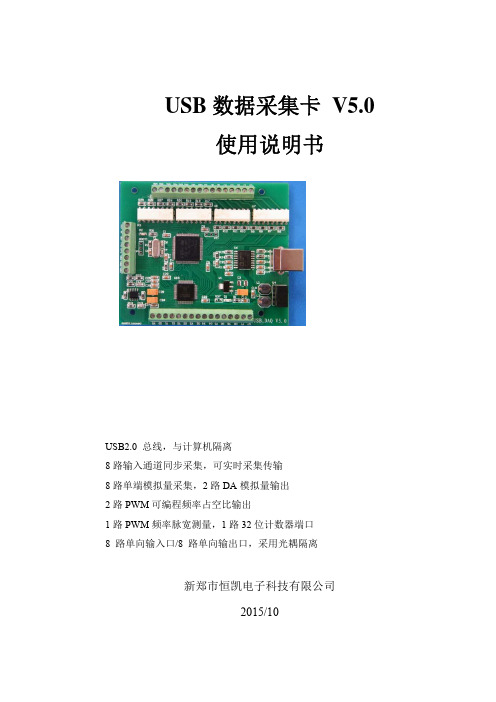
USB数据采集卡 V5.0使用说明书USB2.0 总线,与计算机隔离8路输入通道同步采集,可实时采集传输8路单端模拟量采集,2路DA模拟量输出2路PWM可编程频率占空比输出1路PWM频率脉宽测量,1路32位计数器端口8 路单向输入口/8 路单向输出口,采用光耦隔离新郑市恒凯电子科技有限公司2015/10在开始使用前请仔细阅读下面说明检查打开包装请查验如下:¾USB数据采集卡 V5.0一块;¾高屏蔽USB数据传输电缆一根;保修本产品自售出之日起一年内,用户遵守储存、运输和使用要求,而产品质量不合要求,凭保修单免费维修。
因违反操作规定和要求而造成损坏的,需缴纳器件费及相应的运输费用,如果板卡有明显烧毁、烧糊情况原则上不予维修。
如果板卡开箱测试有问题,可以免费维修(限购买板卡10天内)。
软件支持服务自销售之日起提供6个月的免费开发咨询。
目录一、 USB 数据采集卡V5.0 说明 (1)1.1 板卡简介 (1)1.2 软件支持 (2)1.3 应用领域 (2)1.4 售后服务 (2)二、性能指标 (3)2.1 USB总线性能 (3)2.2 模拟信号输入 (3)2.3 模拟信号输出 (3)2.4 数字信号输入/输出 (3)2.5 PWM测量输入 (4)2.6 计数器 (4)2.7 PWM输出 (4)2.8、工作温度 (4)三、安装与连接 (5)3.1 安装 (5)3.1.1 关于USB (5)3.1.2 USB延长线 (5)3.2 信号连接注意事项 (5)3.4 端子定义及排序说明 (6)3.4 板子尺寸 (7)3.5 各类信号链接方式 (7)四、软件的安装与使用 (10)4.1 驱动的安装与软件的使用 (10)4.1.1 驱动的安装 (10)4.1.2 软件的使用 (12)4.2 接口函数说明 (16)4.2.1 设备操作函数 (16)4.2.2 AD操作函数概况 (17)4.2.3 其它输入输出操作函数 (20)4.2.4 多板卡同时使用相关函数 (23)4.2.5 过采样及相关说明 (24)五、客户程序使用采集卡教程 (28)5.1 VC编程教程 (28)5.2 编程教程 (28)5.3 LABVIEW编程教程 (29)5.4 Labwidows/CVI (32)一、 USB 数据采集卡V5.0 说明恒凯电子-USB数据采集卡采用USB2.0高速总线接口,总线极具易用性,即插即用,是便携式系统用户的最佳选择,可以完全取代以往的PCI卡。
4051系列信号 频谱分析仪用户手册说明书

4051系列信号/频谱分析仪用户手册中电科思仪科技股份有限公司该手册适用下列型号信号/频谱分析仪:●4051A 信号/频谱分析仪(3Hz ~ 4GHz)。
●4051B 信号/频谱分析仪(3Hz ~ 9GHz)。
●4051C 信号/频谱分析仪(3Hz ~ 13.2GHz)。
●4051D 信号/频谱分析仪(3Hz ~ 18GHz)。
●4051E 信号/频谱分析仪(3Hz ~ 26.5GHz)。
●4051F 信号/频谱分析仪(3Hz ~ 40GHz)。
●4051G 信号/频谱分析仪(3Hz ~ 45GHz)。
●4051H 信号/频谱分析仪(3Hz ~ 50GHz)。
●4051L 信号/频谱分析仪(3Hz ~ 67GHz)。
●4051N 信号/频谱分析仪(3Hz ~ 85GHz)。
●4051A-S 信号/频谱分析仪(3Hz ~ 4GHz)。
●4051B-S 信号/频谱分析仪(3Hz ~ 9GHz)。
●4051C-S 信号/频谱分析仪(3Hz ~ 13.2GHz)。
●4051D-S 信号/频谱分析仪(3Hz ~ 18GHz)。
●4051E-S 信号/频谱分析仪(3Hz ~ 26.5GHz)。
4051系列信号/频谱分析仪除标准配件外的选件如下:●4051-H01,后面板射频输入:将射频信号输入接口后置。
●4051-H02,高中频输出:输出频率范围275MHz ~ 475MHz,步进分辨率1Hz,提供30dB增益,1dB步进。
●4051-H03,中频输出:输出频率范围10MHz ~ 160MHz,步进分辨率1Hz,提供4档自动增益控制电平。
●4051-H04A,重构中频/视频信号输出:以数字重构的方式实现任意中频、AM/FM或I/Q信号输出,带宽上限为40MHz。
●4051-H04B,宽带重构中频/视频信号输出:以数字重构的方式实现任意中频、AM/FM或I/Q信号输出,带宽范围为50MHz~100MHz。
●4051-H08,宽带对数检波输出:输出反映输入信号电平特性的对数检波信号。
USB-7411系列硬件说明书

USB-7411系列硬件说明书声明:本手册的版权归北京中泰联创科技有限公司所有,并保留所有的权利。
未经本公司授权,任何公司及个人不得以盈利目的进行复制、抄袭、翻译或传播。
订购产品前,请详细了解产品性能是否符合用户需求。
说明书描述了产品的基本功能,若客户有特殊要求需要增加其他功能,请与本公司工程师联系。
说明书的内容力求准确、可靠。
本公司对侵权使用说明书所造成的后果不承担任何法律责任。
安全使用常识:•使用前,请务必仔细阅读产品用户手册。
•当需要对产品进行操作时请先关闭电源。
•不要带电插拔,以免部分敏感元件被瞬间冲击电压烧毁。
•避免频繁开机对产品造成不必要的损坏。
目录第一章产品介绍 (2)1.1概述 (2)1.1.1USB/RS485/RS232多方式通讯接口 (2)1.1.2模块上16路模拟输入 (2)1.2特点 (2)1.3一般特性 (3)第二章安装与测试 (3)2.1初始检查 (3)2.2跳线分布图 (3)2.3布局说明 (4)2.3.1拨码开关说明 (4)2.3.2指示灯说明 (5)2.3.3终端匹配电阻说明 (5)2.4Windows2K/XP/9X下板卡的安装 (5)2.4.1软件的安装 (5)2.4.2硬件的安装 (6)2.5测试 (7)2.5.1模拟输入功能测试 (8)第三章连接说明 (9)3.1管脚和电位器分布图 (9)3.1.1管脚功能定义说明 (10)3.1.2电位器功能说明 (10)3.2模拟输入连接 (11)3.2.1热电偶输入连接及注意事项 (11)第四章结构说明 (11)第五章常见问题及解决方法 (13)第六章保修说明 (13)第一章产品介绍1.1概述USB7411是远端热电阻采集模块,适用于各类工业现场,可采集16路PT100、Cu50型热电阻,并转换成相应的温度值;通过USB、RS232、RS485三种接口方式,与上位机实时通讯。
1.1.1USB/RS485/RS232多方式通讯接口USB-7411系列除了可以使用USB方式进行数据采集,同时也可以使用RS485/RS232方式进行数据采集,此三种通讯方式可以同时使用。
USB-4711A使用手册
目录1. 介绍 (3)1.1 概述 (3)1.2I/O 接口 (3)1.3 针脚定义 (3)1.4 模拟量输入连接 (5)1.4.1 单端通道连接 (5)1.4.2 差分输入连接 (5)1.5 模拟量输出连接(电压) (6)1.6 触发源连接 (7)1.6.1 内部脉冲触发连接 (7)1.6.2 外部触发源连接 (7)2. 研华设备驱动应用 (7)3. 函数参考 (8)3.1USB系列函数支持列表 (8)3.1.1Device 函数组 (8)3.1.2 模拟量输入函数组 (8)3.1.3 模拟量输出函数组 (8)3.1.4 数字量输入/输出函数组 (8)3.1.5Counter 函数组 (8)4. 使用函数 (9)4.1 设备函数组 (9)4.1.1DRV_DeviceOpen (11)4.1.2DRV_DeviceClose (11)4.2 模拟量输入函数组 (12)4.2.1DRV_AIConfig (13)4.2.2DRV_AIV oltageIn (14)4.2.3DRV_AIBinaryIn (15)4.2.4DRV_AIScale (16)4.3 模拟量输出函数组 (17)4.3.1DRV_AOConfig (18)4.3.2DRV_AOV oltageOut (20)4.3.3DRV_AOBinaryOut (21)4.3.4DRV_AOScale (22)4.4Counter 函数组 (23)4.4.1DRV_CounterEventStart (24)4.4.2DRV_CounterEventRead (25)4.4.3DRV_CounterReset (26)5.VC中使用研华设备驱动编程指南 (28)5.1 添加必要文件 (30)5.2 编写代码 (31)5.3 测试程序 (32)1. 介绍1.1 概述USB-4711A系列包括即插即用数据采集模块,因此无需再打开您的计算机机箱来安装板卡。
研华工业USB IO模块
USB-4622 5端口USB 2.0集线器概述USB-4622是一个USB 2.0集线器,它能够连接最多5个USB从模块。
支持USB 2.0高速模式,可以达到480Mbps的数据转换速率,以实现USB-4700系列在大负载环境中的高性能应用。
研华独特的锁紧式USB电缆设计保证了从模块的连接,防止了电缆偶然的脱落。
特点5个USB 2.0端口(A型)兼容USB 2.0/1.1/1.0480M/s高速数据转换LED指示灯适合DIN导轨安装缩紧式USB电缆用于紧固连接规格接口 1个上游(B型)/5个下游(A型)兼容性 USB总线规格Rev.2.0/1.1/1.0先进的配置与电源接口 (ACPI), OnNow与USB电源管理需求转换速率 480Mbps(高速模式)12Mbps(全速模式)1.5Mbps(低速模式)供电电流每通道最大500mA一般规格外壳塑料(ABS+PC)尺寸132×80×32mm(L×W×H)功耗最大+5V @ 2.5A工作温度0 ~ 60° C (32 ~ 140° F) (参考 IEC 68-2-1, 2)存储温度 -20 ~ 70° C (-4 ~ 158° F)存储湿度 5~95%,RH, 无凝结(参考 IEC 68-2-3)订货信息USB-4622 5端 口USB 2.0集线器(包括电源适配器)USB-4711 100kS/s,12位多功能USB模块概述USB-4700系列包括即插即用数据采集模块,因此无需再打开您的计算机机箱来安装板卡。
仅需插上模块,便可以采集到数据。
它在工业应用中足够可靠和稳定,却并不昂贵。
USB-4700是增加任何带有USB端口的计算机测量和控制能力的最佳的途径。
USB-4711是完全的即插即用设计,便于使用。
它通过USB端口获得所有所需的电源,无需外部的电源连接。
特点支持USB 2.0便携设计总线供电16路模拟输入通道12位分辨率采样速率高达150kS/s8路DI, 8路DO, 2路AO和1路32位计数器带有接线端子适合DIN导轨安装锁紧式USB电缆用于紧固式连接规格模拟输入通道 USB-4711: 16 路单端分辨率 12 位最大采样速率 USB-4711: 最大100kS/sFIFO大小 1024 samples过压保护 30 Vp-p输入电阻 USB-4711: 2 MΩ采样模式软件,可编程pacer或外部脉冲输入范围 (V,软件可编程)极性电压± 10 ± 5 ± 2.5 ± 1.25 ± 0.625精度(% of FSR ±1LSB) 0.1 0.1 0.2 0.2 0.4*注:采样速率和吞吐量依赖于计算机硬件结构和软件环境,速率会根据编程语言、代码效率、CPU利用率等因素发生变动。
过控实验指导书(USB-4711A)
实验一过程控制系统简介及过程控制演示一、组合式过程控制系统介绍结合过程计算机控制系统理论的学习,我们研制了一套组合式过程控制系统,这套系统可以通过灵活、方便的管路组合,实现过程控制中的五种典型控制方式—单回路控制,串级控制、前馈控制、均匀控制和比值控制。
二、主要仪器与设备1、计算机2、接口板卡USB-4711AUSB-4711A系列板卡是即插即用数据采集模块,它通过USB端口与计算机相连,为数据测量与系统控制提供了便利。
USB-4711A通过USB端口获得所需电源,在该板卡上包含了所有的数据采集功能,如:16路AI,2路AO,8路DI,8路DO,1路32位计数器,其中A/D数据采集为12位。
USB-4711A 板卡如图1-1所示。
图1-2为USB-4711A 上五个10针I/O 接口的针脚定义。
图1-1 USB-4711A板卡DO0DO1DO2DO3DGNDDO4DO5DO6DO7DGNDDI0DI1DI2DI3DGNDAI0GATE DGND EXTTRG DGND EVTINPOut AGND AO1AGNDDI4DI5DI6DI7 DGNDAI1AI2AI3AGNDAI4AI5AI6AI7AGNDAI8AI9AI10AI11AGNDAI12AI13AI14AI15AGNDAO0USBLED8-TTL DO Port8-TTL DI Port16-SE/8-Diff AIExternal Control2-AO Port图1-2I/O 接口针脚定义3、水箱:水箱如图1-3所示,技术参数见表1-1。
表1-1 水箱参数工作温度最大:+65CO外部尺寸宽度深度高度240 mm 190 mm 385 mm材质塑料图1-3 水箱4、流量传感器流量传感器如图1-4所示,主要技术参数见表1-2。
表1-2 流量传感器技术参数工作电压 5 to 12 V DC工作电流 6 to 33 mA输出信号方波信号,5…12 V频率范围13 to 1200 HZ测量范围0.5 to 15.0 l/min工作压力80°C max。
PT4711A;PT4711C;PT4711N;中文规格书,Datasheet资料
For technical support and further information, visit Features•Input Voltage: 36 V to 75 V •Dual Output (15 V / 15 V)(Independently Regulated!)•Separate Output Returns(Accommodates ±15 V or +30 V)•Internal Power-Up Sequencing •Flexible On/Off Control •Output Current Limit•Fixed Frequency Operation•Over-T emperature Shutdown •Under-Voltage Lockout •1500 VDC Isolation•Space-Saving Solderable Case 1.2 sq. in. PCB Area (suffix N)•Surface Mount Option•Safety Approvals (Pending):UL 60950, cUL 60950For technical support and further information, visit On/Off Enable LogicPin DescriptionsPin 3Pin 4Output Status×1Off 10On 0×OffNotes:Logic 1 =Open collectorLogic 0 = –Vin (pin 2) potentialFor positive Enable function, connect pin 4to pin 2 and use pin 3.For negative Enable function, leave pin 3open and use pin 4.+Vin: The positive input supply for the module with respect to –V in . When powering the module from a –48-V telecom central office supply, this input is connected to the primary system ground.–Vin: The negative input supply for the module, and the 0-VDC reference for the EN 1, and EN 2 inputs.When powering the module from a +48-V supply,this input is connected to the input source return.EN 1: The negative logic input that activates the module output. This pin must be connected to –V in to enable the module’s outputs. A high impedance disables the module’s outputs.EN 2: The positive logic input that activates the module output. If not used, this pin should be left open circuit. Connecting this input to –V in disables the module’s outputs.+Vo 1: This is the positive DC output voltage with respect to –Vo 1. The output voltage produced across ±Vo 1 is electrically isolated from ±V in and indepen-dently regulated from that produced at ±Vo 2. If the +Vo 1 node is connected to the secondary ground, a negative output voltage will be produced at –Vo 1.–Vo 1: The negative output supply voltage with respect to +Vo 1. If this node is connected to the secondary ground, a positive voltage is produced at +Vo 1.+Vo 2: This is the positive DC output voltage with respect to –Vo 2. The output voltage produced across ±Vo 2 is electrically isolated from ±V in and indepen-dently regulated from that produced at ±Vo 1. If +Vo 2node is connected to the secondary ground, a nega-tive output voltage will be produced at –Vo 2.–Vo 2: The negative output supply voltage with respect to +Vo 2. If this node is connected to the secondary ground, a positive voltage is produced at +Vo 2.±Vo 1 Adjust: Using a single resistor, this pin allows the output voltage produced at ±Vo 1 to be adjusted higher or lower by up to 10%. If not used this pin should be left open circuit.±Vo 2 Adjust: Using a single resistor, this pin allows the output voltage produced at ±Vo 2 to be adjusted higher or lower by up to 10%. If not used this pin should be left open circuit.Pin Function8Pin Not Present 9Pin Not Present 10Pin Not Present 11Pin Not Present 12Pin Not Present 13Pin Not Present 14+Vo 1Pin ConfigurationNote:Shaded functions indicates those pins that are at primary-sidepotential. All other pins are referenced to the secondary.Pin Function15Not Connected 16–Vo 117Vo 1 Adjust 18+Vo 219Not Connected 20–Vo 221Vo 2 AdjustPT4711 Electrical Specifications(Unless otherwise stated, the operating conditions are:- TNotes:(1)The Enable inputs (pins 3 & 4) have internal pull-ups. Leaving pin 3 open-circuit and connecting pin 4 to –V in allows the the converter to operate when input power is applied. The maximum open-circuit voltage is 5 V.(2)The maximum voltage that may exist between any two output pins.(3)See SOA curves or consult factory for appropriate derating.(4)During solder reflow of SMD package version, do not elevate the module case, pins, or internal component temperatures above a peak of 215°C. Forfurther guidance refer to the application note, “Reflow Soldering Requirements for Plug-in Power Surface Mount Products,” (SLT A051).(5)Only the case pins on through-hole pin configurations (N & A) must be soldered. For more information see the applicable package outline drawing.For technical support and further information, visit For technical support and further information, visit Typical CharacteristicsNote A: All Characteristic data in the above graphs has been developed from actual products tested at 25°C. This data is considered typical data for the ISR.Note B: SOA curves represent operating conditions at which the internal components are at or below the manufacturer’s maximum rated operating temperatures.C r o s s R e g u l a t i o n V o 1 (V )C r o s s R e g u l a t i o n |V o 2| (V )45-W Dual-Output Isolated E f f i c i e n c y - %P d - W a t t sOperating Features of the PT4711Dual-Output DC/DC ConverterOver-Current ProtectionEach of the two outputs from the PT4711 DC/DC con-verter incorporates protection against an output load fault. When a fault impedance is applied to one output, the module initially limits the output current of that output to approximately 150% of the maximum current rating. If the fault persists for more than 20 ms the con-verter shuts down, forcing the voltage at both regulated outputs to simultaneously fall to zero. Following shutdown the converter periodically attempts to recover by executing a soft-start power-up. The converter will contine in a cycle of successive shutdowns and restarts until the load fault is removed.Over-Temperature ProtectionThe PT4711 DC/DC converter has an internal tem-perature sensor, which monitors the temperature of the module’s internal components. If the sensed temperature exceeds a nominal 115°C, the converter will shut down. The converter will automatically restart when the sensed temperature returns to about 100°C.Under-Voltage Lock-OutThe Under-Voltage Lock-Out (UVLO) circuit prevents operation of the converter whenever the input voltage to the module is insufficient to maintain output regulation. The UVLO has approximately 2 V of hysterisis. This is to prevent oscillation with a slowly changing input volt-age. Below the UVLO threshold the module is off and the enable control inputs, EN1 and EN2 are inoperative.Primary-Secondary IsolationThe PT4711 DC/DC converter incorporates electrical isolation between the input terminals (primary) and the output terminals (secondary). All converters are production tested to a withstand voltage of 1500 VDC. The isolation complies with UL/cUL 60950 and EN60950, and the requirements for operational isolation. This allows the converter to be configured for either a positive or nega-tive input voltage source.The regulation control circuitry for these modules is located on the secondary (output) side of the isolation barrier. Control signals are passed between the primary and secondary sides of the converter. The data sheet ‘Pin Descriptions’ and ‘Pin-Out Information’ provides guid-ance as to which reference (primary or secondary) that must be used for each of the external control pin.Input Current LimitingThe converter is not internally fused. For safety and overall system protection, the maximum input current to the converter must be limited. Active or passive current limiting can be used. Passive current limiting can be a fast acting fuse. A 125-V fuse, rated no more than 5 A, is recommended. Active current limiting can be imple-mented with a current limited “Hot-Swap” controller. Output Voltage ConfigurationsBoth outputs from the PT4711 DC/DC converter are independently regulated and isolated from each other. This allows flexibility to how the output voltages may be configured (up to the maximum allowed working voltage between the two outputs; see specification table). Figure 1-1 shows the most common ways that the outputs of the converter may be configured. They include ±V o (Fig. 1-1a), V o(a)/V o(b) (Fig. 1-1b), and 2 × V o (Fig. 1-1c).For technical support and further information, visit For technical support and further information, visit Figure 3-3; PT4711 Power-up SequenceOn/Off Output Voltage SequencingBoth outputs from the PT4711 converter are internally sequenced to power up in unison. Figure 3-3 shows the output waveforms after the module’s output has been enabled. The converter produces a fully regulated output within 75 ms. The waveforms were measured with the output voltages configured per Figure 1-1a (for ±15-V output). A constant current load of 1.5 A was applied to both outputs, with an input source of 48 VDC.Using the On/Off Enable Controls on the PT4711Dual-Output DC/DC ConverterThe PT4711 is a dual-output DC/DC converter incor-porates two output enable controls. EN1 (pin 4) is the Negative Enable input, and EN2 (pin 3) is the Positive Enable input. Both inputs are electrically referenced to -V in (pin 2) on the primary or input side of the converter.A pull-up resistor is not required, but may be added if desired. Voltages of up to 70 V can be safely applied to the either of the Enable pins.Automatic (UVLO) Power-UpConnecting EN1 (pin 4) to -V in (pin 2) and leaving EN2(pin 3) open-circuit configures the converter for auto-matic power up. (See data sheet “T ypical Application”).The converter control circuitry incorporates an “Under Voltage Lockout” (UVLO) function, which disables the converter until the minimum specified input voltage is present at ±V in . (See data sheet Specifications). The UVLO circuitry ensures a clean transition during power-up and power-down, allowing the converter to tolerate a slow-rising input voltage. For most applications EN1 and EN2,can be configured for automatic power-up.Positive Output Enable (Negative Inhibit)T o configure the converter for a positive enable function,connect EN1 (pin 4) to -V in (pin 2), and apply the system On/Off control signal to EN2 (pin 3). In this configura-tion, a low-level input voltage (-V in potential) applied to pin 3 disables the converter outputs. Figure 1 is an example of this configuration.Negative Output Enable (Positive Inhibit)T o configure the converter for a negative enable function,EN2 (pin 3) is left open circuit, and the system On/Off control signal is applied to EN1 (pin 4). A low-level input voltage (-V in potential) must then be applied toFigure 2; Negative Enable ConfigurationFigure 1; Positive Enable Configurationpin 4 in order to enable the outputs of the converter.An example of this configuration is detailed in Figure 2.Note: The converter will only produce an output voltage if a valid input voltage is applied to ±V in .+Vo (5 V/Div)1+Vo (5 V/Div)2HORIZ SCALE: 5 ms/DivFor technical support and further information, visit Adjusting the Output Voltages of the PT4711Dual-Output DC/DC ConvertersThe PT4711 dual-output DC/DC converter produces two independently regulated output voltages. The mag-nitude of each output may be trimmed higher or lower than the nominal set-point by up to 10%. The adjust-ment method uses a single external resistor. 1 The value of the resistor determines the magnitude of adjustment,and the location of the resistor determines the direction of adjustment (increase or decrease). The resistor values can be calculated using a formula (see below). Alterna-tively the resistor value may be selected directly from the values given in T able 2-2. The placement of each resistor is as follows.Adjust Up: To increase the magnitude of the output volt-age, add a resistor R 1 between the appropriate Vo x Adj (‘Vo 1 Adj’ or ‘Vo 2 Adj’) and the respective -Vo x voltage rail. See Figure 2-1(a) and T able 2-1 for the resistor placement and pin connections.Figure 2-1bCalculation of Resistor Adjust ValuesThe adjust resistor value may also be calculated using an equation. Note that the equation for R 1 [Adjust Up] is different to that for (R 2) [Adjust Down].R 1 [Adjust Up]=35.75– 20k Ω(V a – V o )(R 2) [Adjust Down]=14.3 (V a – 2.5)– 20k Ω(V o – V a )Where:V o = Original output voltage (Vo x )V a = Adjusted output voltage (Va x )12 lower1, or Vo 2+Vo x–Vo xFigure 2-1a12 higher1, or Vo 2+Vo x–Vo xAdjust Down: T o decrease the magnitude of the output voltage, add a resistor (R 2), between the appropriate V o x Adj (Vo 1 Adj or Vo 2 Adj,) and the respective +Vo x voltage rail. See Figure 2-1(b) and T able 2-1 for the resistor placement and pin connections.Table 2-1; Adjust Resistor Pin ConnectionsTo Adjust Up To Adjust DownConnect R 1Connect (R 2)from to from to Vo x Adj–Vo xVo x Adj+Vo xV o 117161714V o 221202118Notes:e only a single 1% (or better) tolerance resistor in either the R 1 or (R 2) location to adjust a specific output.Place the resistor as close to the ISR as possible.2.Never connect capacitors to any of the ‘Vo x Adj’ pins. Any capacitance added to these control pins will affect the stability of the respective regulated output.For technical support and further information, visit Table 2-2ADJUSTMENT RESISTOR VALUES FOR Vo 1 & Vo 2Adj. ResistorR 1/(R 2)% Adjust V a (req’d)–10%13.50 V (84.9) k Ω– 9%13.65 V (98.1) k Ω– 8%13.80 V (115) k Ω– 7%13.95 V (136) k Ω– 6%14.10 V (164) k Ω– 5%14.25 V (204) k Ω– 4%14.40 V (264) k Ω– 3%14.55 V (363) k Ω– 2%14.70 V (562) k Ω– 1%14.85 V (1.16) M Ω 0%15.00 V + 1%15.15 V 218 k Ω+ 2%15.30 V 99.2 k Ω+ 3%15.45 V 59.4 k Ω+ 4%15.60 V 39.6 k Ω+ 5%15.75 V 27.7 k Ω+ 6%15.90 V 19.7 k Ω+ 7%16.05 V 14.0 k Ω+ 8%16.20 V 9.8 k Ω+ 9%16.35 V 6.5 k Ω+10%16.50 V 3.8 k ΩR 1 = Black, R 2 = (Blue)PT4711PACKAGAddendum-Page 1PACKAGING INFORMATIONOrderable DeviceStatus(1)Package Type PackageDrawingPins Package QtyEco Plan(2)Lead/Ball Finish MSL Pea PT4711A OBSOLETE SIP MODULE ENN 21TBDCall TI Call TIPT4711CNRNDSIP MODULEENP218TBD Call TILevel-3-215C(1)The marketing status values are defined as follows:ACTIVE: Product device recommended for new designs.LIFEBUY: TI has announced that the device will be discontinued, and a lifetime-buy period is in effect.NRND: Not recommended for new designs. Device is in production to support existing customers, but TI does not recommend using this part in a new PREVIEW: Device has been announced but is not in production. Samples may or may not be available.OBSOLETE: TI has discontinued the production of the device.(2)Eco Plan - The planned eco-friendly classification: Pb-Free (RoHS), Pb-Free (RoHS Exempt), or Green (RoHS & no Sb/Br) - please check http://www.t information and additional product content details.TBD: The Pb-Free/Green conversion plan has not been defined.Pb-Free (RoHS): TI's terms "Lead-Free" or "Pb-Free" mean semiconductor products that are compatible with the current RoHS requirements for all lead not exceed 0.1% by weight in homogeneous materials. Where designed to be soldered at high temperatures, TI Pb-Free products are suitable fo Pb-Free (RoHS Exempt): This component has a RoHS exemption for either 1) lead-based flip-chip solder bumps used between the die and package, the die and leadframe. The component is otherwise considered Pb-Free (RoHS compatible) as defined above.Green (RoHS & no Sb/Br): TI defines "Green" to mean Pb-Free (RoHS compatible), and free of Bromine (Br) and Antimony (Sb) based flame retard in homogeneous material)(3)MSL, Peak Temp. -- The Moisture Sensitivity Level rating according to the JEDEC industry standard classifications, and peak solder temperature.Important Information and Disclaimer:The information provided on this page represents TI's knowledge and belief as of the date that it is provided. TI provided by third parties, and makes no representation or warranty as to the accuracy of such information. Efforts are underway to better integrate inf continues to take reasonable steps to provide representative and accurate information but may not have conducted destructive testing or chemical an TI and TI suppliers consider certain information to be proprietary, and thus CAS numbers and other limited information may not be available for releasIn no event shall TI's liability arising out of such information exceed the total purchase price of the TI part(s) at issue in this document sold by TI to Cu/分销商库存信息:TIPT4711A PT4711C PT4711N。
研华USB-4711中文使用手册
图 2.11: 设备测试对话框内的 Counter 标签................19
2.6
拆卸硬件.......................................................20
图 2.12: 拔除或弹出硬件对话框..........................20
1.3
安装指南........................................................3
图 1.1: 安装流程图.....................................4
1.4
软件概述........................................................5
3.5.1 内部脉冲触发连接 ....................................... 27 3.5.2 外部触发源连接 ......................................... 27
3.6
现场接线考虑因素 .............................................. 28
Material Authorization) 序列号。这可以让我们尽快地进行故障产品的回收。 4. 请仔细地包装故障产品,并在包装中附上完整的售后服务卡片和购买日期证明
(如销售发票)。我们对无法提供购买日期证明的产品不提供质量保证服务。 5. 把相关的 RMA 序列号写在外包装上,并将其运送给销售人员。
A.2
模拟量输出 .................................................... 30
VC++和数据采集卡编程开发2——基础部分
规格和功能说明
模拟量输入:数据传输方式 - 软件轮询方式:
▪ 前台操作,方便灵活 ▪ 无法以固定速率采集
- 中断方式: ▪ 后台操作 ▪ CPU针对一定数量的采集点数响应中断
▪ 最快可达200kS/s (USB-4716) - DMA方式:
Analog Data
采样 & 保持
数量化
AD Converter
Digital Data
数据采集控制卡的工作原理
模拟量输入:模拟量到数字量转换器 (ADC) - 分辨率:The no. of levels is 2resolution 1LSB = Range/ 2resolution
– Ex: 8bit→20V/256=0.08V=80mV
优、缺点
– 良好的散热性、抗震动性、抗冲击 – 可热插拔 – 最多可以支持256个PCI总线设备 – 用户可以自由选择前出线或者后出线方式 – 隐蔽的总线仲裁,减小了仲裁开销。
MIC系列板卡举例: MIC-3714
30 MS/s 四通道同步模拟量采集卡
特点 • 12位A/D转换器,最高可达30MS/s采集速
规格和功能说明
模拟量输入:输入模式 - 单端模式下, 电压输入的参考端为同一个地 - 差分模式下,差分通道的配对是固定的 (ch0 & ch1, ch2
& ch3, …, ch14 & ch15). - 差分模式下的通道数只有单端模式的一半。 - 某些板卡允许混合输入的模式
Single Ended
100KS/s • 量程可以程序设定 • 自动通道/增益扫描 • 板载1KFIFO缓存 • 16路数字量输入,16路数字量输出 • 板载可编程计数器
PCI 总线
- 1、下载文档前请自行甄别文档内容的完整性,平台不提供额外的编辑、内容补充、找答案等附加服务。
- 2、"仅部分预览"的文档,不可在线预览部分如存在完整性等问题,可反馈申请退款(可完整预览的文档不适用该条件!)。
- 3、如文档侵犯您的权益,请联系客服反馈,我们会尽快为您处理(人工客服工作时间:9:00-18:30)。
目录1. 介绍 (3)1.1 概述 (3)1.2I/O 接口 (3)1.3 针脚定义 (3)1.4 模拟量输入连接 (5)1.4.1 单端通道连接 (5)1.4.2 差分输入连接 (5)1.5 模拟量输出连接(电压) (6)1.6 触发源连接 (7)1.6.1 内部脉冲触发连接 (7)1.6.2 外部触发源连接 (7)2. 研华设备驱动应用 (7)3. 函数参考 (8)3.1USB系列函数支持列表 (8)3.1.1Device 函数组 (8)3.1.2 模拟量输入函数组 (8)3.1.3 模拟量输出函数组 (8)3.1.4 数字量输入/输出函数组 (8)3.1.5Counter 函数组 (8)4. 使用函数 (9)4.1 设备函数组 (9)4.1.1DRV_DeviceOpen (11)4.1.2DRV_DeviceClose (11)4.2 模拟量输入函数组 (12)4.2.1DRV_AIConfig (13)4.2.2DRV_AIV oltageIn (14)4.2.3DRV_AIBinaryIn (15)4.2.4DRV_AIScale (16)4.3 模拟量输出函数组 (17)4.3.1DRV_AOConfig (18)4.3.2DRV_AOV oltageOut (20)4.3.3DRV_AOBinaryOut (21)4.3.4DRV_AOScale (22)4.4Counter 函数组 (23)4.4.1DRV_CounterEventStart (24)4.4.2DRV_CounterEventRead (25)4.4.3DRV_CounterReset (26)5.VC中使用研华设备驱动编程指南 (28)5.1 添加必要文件 (30)5.2 编写代码 (31)5.3 测试程序 (32)1. 介绍1.1 概述USB-4711A系列包括即插即用数据采集模块,因此无需再打开您的计算机机箱来安装板卡。
仅需插上模块,便可以采集到数据,简单高效。
USB-4711A 是给任何带有USB端口的计算机增加测量和控制能力的最佳途径。
它通过USB 端口获得所有所需的电源,因此无需连接外部的电源。
USB-4711A在一块卡上包含了所有的数据采集功能,如:16路AI,2路AO,8路DI,8路DO,1路32位计数器,其中A/D数据采集为12位。
USB-4711A板卡如图1.1所示。
图1.1 USB-4711A板卡1.2I/O 接口USB-4711A 配有插入式螺丝端子接口,因此连接模块时无需另外准备端子板或电缆。
1.3 针脚定义图 1.2为USB-4711A 上五个10针I/O 接口的针脚定义。
两个接地参考AGND 和DGND 的用途不同,因此应分开使用。
不要将两者进行连接。
表1.1为I/O 接口信号的描述。
DO0DO1DO2DO3DGNDDO4DO5DO6DO7DGNDDI0DI1DI2DI3DGNDAI0GATE DGND EXTTRG DGND EVTINPOut AGND AO1AGNDDI4DI5DI6DI7 DGNDAI1AI2AI3AGNDAI4AI5AI6AI7AGNDAI8AI9AI10AI11AGNDAI12AI13AI14AI15AGNDAO0USBLED8-TTL DO Port8-TTL DI Port16-SE/8-Diff AI External Control2-AO Port图 1.2I/O 接口针脚定义表 1.1I/O 接口信号描述1.4 模拟量输入连接USB-4711A支持16 路单端/8路差分输入。
每个输入通道都可通过软件方式进行选择。
1.4.1 单端通道连接单端输入配置只为每个通道提供1根信号线,且被测电压(Vm)是以公共地为参考的线缆电压。
没有接地端的信号源称为“浮动信号源”。
将单端通道连接至浮动信号源尤为简单。
在这种模式下,USB-4711A 为外部浮动信号源提供一个参考地。
图1.3为浮动信号源与USB-4711A的1个输入通道的单端通道连接。
图1.3 单端输入通道连接1.4.2 差分输入连接差分输入为每个通道提供两根信号线,两根信号线之间的电压差是可测量的。
在USB-4711A中,当所有通道都配置为差分输入,最多可有8个模拟通道。
如果信号源的一侧连接到地面,信号源作为参考地。
因此,信号源的地与板卡地将形成不完全相同的电压。
地面之间的电压差异,形成了一个共模电压(V cm )。
为了避免共模电压引起的接地回路噪声的影响,您可以连接到低输入信号地面。
注:在差分输入模式,输入通道n应使用通道n +1。
(N =0,2,4... 14)图1.4为USB-4711A的1个输入通道的差分输入通道连接。
图1.4 差分输入通道连接1.5 模拟量输出连接(电压)USB-4711A提供了2个模拟量输出通道,即AO0和AO1。
图 1.5 为USB-4711A的模拟量输出通道连接。
图1.5 模拟量输出通道连接1.6 触发源连接1.6.1 内部脉冲触发连接USB-4711A提供了2个16-bit计数器,可以连接至1个10MHz 时钟。
计数器0负责输入通道的事件计数。
计数器1是1个16-bit定时器,用于脉冲触发。
计数器1输出的上升沿信号(低—高)将触发USB-4711A的A/D 转换。
1.6.2 外部触发源连接除脉冲触发以外,USB-4711A还为A/D 转换提供了外部触发。
将GATE信号连接至+5V DC 源时,外部触发功能即被禁用。
断开与+5VDC源的连接即可启用外部触发功能。
2. 研华设备驱动应用研华Windows设备驱动是动态链接的。
以下列出了开发应用时必需的文件:3.1USB系列函数支持列表3.1.1Device 函数组3.1.2 模拟量输入函数组3.1.3 模拟量输出函数组3.1.4 数字量输入/输出函数组3.1.5Counter 函数组函数描述函数部分包括模拟量输入函数,模拟量输出函数,数字量输入函数,数字量输出函数等等。
研华的每个函数都将以如下形式出现:status = FUNCTION_Name (parameter 1, parameter 2,... , parameter n)(n>0),每个函数都会返回一个状态,表明函数执行成功还是失败(保存在status变量中)。
Status是一个4字节的整型变量,在DRIVER.H里被定义。
4.1 设备函数组进行所有I/O 操作时,必须首先调用DRV_DeviceOpen,通过设备号(Device Number)打开设备得到设备句柄,以使用户访问该设备,然后调用一系列函数执行相应的功能。
结束操作时,调用DRV_DeviceClose关闭设备,释放由DRV_DeviceOpen分配的资源,基本流程如图4.1所示。
图4.1 设备函数组应用流程Device Number (Type:Unsigned Long,Size:4 bytes)指定要进行I/O操作的设备,即要打开的设备的设备号。
设备号在Advantech Device Manager中初始化设备的时候分配。
比如“000:Advantech DEMOI/O=1H”,这个设备的设备号就为000,用户可以直接在DRV_DeviceOpen函数中指定要打开的设备号,也可以通过调用DRV_SelectDevice 函数打开一个对话框选择需要的设备,从而取得相应的设备号。
DRV_DeviceOpen 和DRV_DeviceClose 函数DRV_DeviceOpen 打开设备号(Device Number)指定的设备。
在I/O操作中,其它函数执行前必须先调用此函数。
与之对应,DRV_DeviceClose 函数用来关闭设备。
Driver Handle (Type:Long,Size:4 bytes)指向的缓存保存了设备的设置信息。
函数DRV_DeviceOpen返回句柄(Driver Handle),其它进行I/O相关操作的函数使用该句柄来指定设备。
Error Code(Type:Unsigned Long,Size:4 bytes)驱动函数返回错误代码(Error Code)来表明函数执行是否成功。
当返回代码非零时,函数执行失败。
DRV_GetErrorMessage函数DRV_GetErrorMessage函数通过错误代码获取出错信息。
4.1.1DRV_DeviceOpenLRESULT DRV_DeviceOpen (ULONG DeviceNum,LONG * DriverHandle ); 用途:通过指定的设备号(DeviceNum)来打开一个已经安装的设备,返回设备句柄DriverHandle以备后续操作。
与指定设备相关的所有操作都必须使用指向该设备的句柄(DriverHandle),所以用户在使用与设备所分配资源相关的任何一项操作,如DIO、AO、AI等之前,必须先调用此函数。
参数:返回值:1. SUCCESS:执行成功。
2. LoadLibraryFailed:动态链接库装载失败,请尝试重新安装驱动程序。
3. MemoryAllocateFailed:驱动程序内部内存分配失败。
4. ConfigDataLost:从注册表获取设备配置信息失败,这些信息可能已经丢失,请尝试重新安装驱动程序。
5. GetProcAddressFailed:无法获得驱动程序函数地址,请尝试更新驱动程序。
注意事项:与设备所分配资源相关的任何一项操作,如DIO、AO、AI等,执行完毕后,用户必须调用DRV_DeviceClose函数来释放由该设备通过DRV_DeviceOpen 分配的资源,为设备再次操作做好准备。
4.1.2DRV_DeviceCloseLRESULT DRV_DeviceClose ( LONG * DriverHandle );用途:关闭由设备句柄DriverHandle 指向的设备,释放为该设备分配的资源。
所有与设备分配资源相关的操作,如:DIO、AO、AI等完成后需要关闭该设备,以释放由函数DRV_DeviceOpen 为该设备分配的资源。
参数:返回值:1. SUCCESS:执行成功。
2. InvalidDriverHandle:设备句柄DriverHandle为NULL。
4.2 模拟量输入函数组软件方式:该组函数通过软件命令触发数据转换。
设备驱动为单通道和多通道数据采集分别提供了不同的函数,两种数据采集都是一次完成。
可以使用软件定时器来周期性地调用这些函数,对单通道或多通道周期性地进行采样。
对于大块数据的连续高速采样,可以采用中断或DMA传输方式。
单通道采样:DRV_AIConfig 函数为指定通道设置输入值范围。