单节锂电池保护芯片
TP4100_TP4101 1000mA、500mA 线性单节锂电池充电放电保护IC

7
充电用于 USB 或小功率电源适配器、太阳 能电池来做电源,而避免电源复位或重启。
电。充满电压固定于 4.2V,而充电电流可通过一个电阻器进行外部设置。当电池达到
4.2V 之后,充电电流降至设定值 1/10,TP4100 将自动终止充电。
TP4100 的放电管理包含了欠压保护、过充保护、输出短路保护、输出过流保护、
芯片过温保护以及多种保护后的延时自激活恢复,其他特点包括充电电流监控器、欠压
充电电流的设定
充电电流是采用一个连接在 PROG 引 脚与地之间的电阻器来设定的。设定电阻器 和充电电流采用下列公式来计算: 根据需要的充电电流来确定电阻器阻值,
公式:
RPROG
900 I BAT
建议客户使用 1%精度电阻用于设置 电流,电阻的偏差直接影响电流的一致性。 不同环境测试电流与公式计算理论值也变 的不完全一致。为了方便客户应用,可根据 下表需求选取合适大小的 RPROG。
STDBY 引脚漏电流
VSTDBY=5V(待机模式)
ቤተ መጻሕፍቲ ባይዱ
STDBY 引脚输出低电平 ISTDBY=5mA
0.3
0.6
V
0
1
μA
0.3
0.6
V
3
ΔVRECHRG TLIM RON
tss tRECHARGE
tTERM IPROG IBAT RBP VOD
再充电电池门限电压 限定温度模式中的结温 功率 FET“导通”电阻 (在 VCC 与 BAT 之间) 软启动时间
VOC
过充保护电压
VOV
IOCP
TBP TCLK TCLKP
非充电状态下 BP 过压
放电输出过流保护
锂电保护芯片CT2101 说明书

过充电流检测延迟时间
tOCC
VDD = 3.5V 7.5
七.功能描述:
CT2101监控电池的电压和电流,并通过断开充电器或者负载,保护单节可充电锂电池不会因为过充 电压、 过放电压、 过放电流以及短路等情况而损坏。 这些功能都使可充电电池工作在指定的范围内; CT2101 支持四种运行模式:正常工作模式、充电工作模式、放电工作模式和休眠工作模式。 1. 正常工作模式 在正常状态下,CT2101由电芯供电,其V 端电压在过充检测电压V 和过放检测电压V 之间,VM端电
DL HD
5. 过放电流情况(过放电流 1和过放电流 2的检测 )
在正常条件下对电池进行放电,当放电电流超过过放检测电流I
检测延迟时间t 态。 恢复条件: 断开负载后电路将自动恢复到正常状态。 6. 负载短路电流情况 或者t
ODC1
或者I
ODC2
,并且维持时间超过过放电流
ODC1
ODC2
时,CT2101将关闭内部开关管,断开放电回路停止放电,进入过放电流保护状
tCU
tDL
tODC1
间 过放电流2检测延迟时
VDD = 3.5V
tODC2
间
VDD = 3.5V
Rev 1.2
2009-12-19
- 5 -
220 负载短路检测延迟时间
320 320 10 10
380 µS 540 12 mS 13.5
tSHORT
VDD = 3.5V 150 8
- 3 -
推荐工作范围
参数 供电电压(VDD 和 GND 间电压) 充电器输入电压(VM 和 GND 间电压) 工作温度范围 符号 VDD VM TOPR 最小值 2.0 -0.3 -40 最大值 5.0 5.5 85 单位 V V ℃
锂电保护芯片 DW

30
50
100
K
CO pin Nch ON voltage CO Nch ON 电压
VCOL
-
0.4
0.5
V
CO pin Pch ON voltage CO Pch ON 电压
VCOH
VDD-0.1 VDD-0.02
-
V
DO pin Nch ON voltage DO Nch ON 电压
VDOL
-
Operation mode 正常操作
Typ. 2.4 μA Max. 6.0 μA (25℃)
Standby mode 待机电流
Green-mode 休眠功能 Self-recovery function 自恢复功能
Max. 0.1 μA (25℃) Max. 3.0 μA (25℃)
Small package 超小型封装
Discharge overcurrent
Detection Voltage [Vdet3]
放电过电流检 测电压
140mV± 30mV
0V Battery Charge Function
0V 充电
Available 允许
Mode Selection
休眠功能 Auto-
recovery 自恢复
◆◆ Electrical Characteristics 电气参数 (无特殊标注时 TA = 25℃ unless otherwise specified)
3
DS-Rev-1.5_cn
DW01A
One-cell Lithium Battery Protection IC
◆◆ Product Name List 产品电压版本
XB5352G 贴片SOT23-5 单节锂电池充电保护芯片 电源管理IC
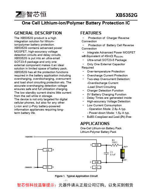
XB5352G ____________________________________________________________________________________________________________________________ One Cell Lithium-ion/Polymer Battery Protection ICGENERAL DESCRIPTIONThe XB5352G product is a high integration solution for lithium-ion/polymer battery protection.XB5352G contains advanced power MOSFET, high-accuracy voltage detection circuits and delay circuits.XB5352G is put into an ultra-smallSOT23-5 package and only oneexternal component makes it an ideal solution in limited space of battery pack. XB5352G has all the protection functions required in the battery application including overcharging, overdischarging, overcurrent and load short circuiting protection etc. The accurate overcharging detection voltage ensures safe and full utilization charging. The low standby current drains little current from the cell while in storage.The device is not only targeted for digital cellular phones, but also for any otherLi-Ion and Li-Poly battery-powered information appliances requiring long-term battery life. FEATURES·Protection of Charger Reverse Connection·Protection of Battery Cell Reverse Connection·Integrate Advanced Power MOSFET with Equivalent of 45mΩ R SS(ON)·Ultra-small SOT23-5 Package ·Only One External Capacitor Required·Over-temperature Protection ·Overcharge Current Protection ·Two-step Overcurrent Detection: -Overdischarge Current-Load Short Circuiting·Charger Detection Function·0V Battery Charging Function- Delay Times are generated inside ·High-accuracy Voltage Detection ·Low Current Consumption- Operation Mode: 2.8μA typ.- Power-down Mode: 1.5μA typ. ·RoHS Compliant and Lead (Pb) FreeAPPLICATIONSOne-Cell Lithium-ion Battery PackLithium-Polymer Battery PackFigure 1. Typical Application CircuitORDERING INFORMATIONNote: “YW” is manufacture date code, “Y” means the year, “W” means the weekPIN CONFIGURATIONFigure 2. PIN ConfigurationPIN DESCRIPTIONABSOLUTE MAXIMUM RATINGS(Note: Do not exceed these limits to prevent damage to the device. Exposure to absolute maximum rating conditions for long periods may affect device reliability.)ELECTRICAL CHARACTERISTICSTypicals and limits appearing in normal type apply for T A= 25o C, unless otherwise specifiedFigure 3. Functional Block Diagram FUNCTIONAL DESCRIPTIONThe XB5352G monitors the voltage and current of a battery and protects it from being damaged due to overcharge voltage, overdischarge voltage, overdischarge current, and short circuit conditions by disconnecting the battery from the load or charger. These functions are required in order to operate the battery cell within specified limits.The device requires only one external capacitor. The MOSFET is integrated andits R SS(ON) is as low as45mΩtypical. Normal operating modeIf no exception condition is detected, charging and discharging can be carried out freely. This condition is called the normal operating mode.Overcharge ConditionWhen the battery voltage becomes higher than the overcharge detection voltage (V CU) during charging under normal conditionand the state continues for the overcharge detection delay time (t CU) or longer, theXB5352G turns the charging control FEToff to stop charging. This condition is called the overcharge condition. The overcharge condition is released in the following two cases:1, When the battery voltage drops below the overcharge release voltage (V CL), the XB5352G turns the charging control FET on and returns to the normal condition.2, When a load is connected and discharging starts, the XB5352G turns the charging control FET on and returns to the normal condition. The release mechanism is as follows: the discharging current flows through an internal parasitic diode of the charging FET immediately after a load is connected and discharging starts, and the VM pin voltage increases about 0.7 V (forward voltage of the diode) from the GND pin voltage momentarily. TheXB5352G detects this voltage and releases the overcharge condition. Consequently, in the case that the battery voltage is equal to or lower than the overcharge detection voltage (V CU), the XB5352G returns to the normal condition immediately, but in the case the battery voltage is higher than the overcharge detection voltage (V CU),the chip does not return to the normal condition until the battery voltage drops below the overcharge detection voltage (V CU) even if the load is connected. In addition, if the VM pin voltage is equal to or lower than the overcurrent 1 detection voltage when a load is connected and discharging starts, the chip does not return to the normal condition.Remark If the battery is charged to a voltage higher than the overcharge detection voltage (V CU) and the battery voltage does not drops below the overcharge detection voltage (V CU) even when a heavy load, which causes an overcurrent, is connected, the overcurrent 1 and overcurrent 2 do not work until the battery voltage drops below the overcharge detection voltage (V CU). Since an actual battery has, however, an internal impedance of several dozens of mΩ, and the battery voltage drops immediately after a heavy load which causes an overcurrent is connected, the overcurrent 1 and overcurrent 2 work. Detection of load short-circuiting works regardless of the battery voltage.Overdischarge ConditionWhen the battery voltage drops below the overdischarge detection voltage (V DL) during discharging under normal condition and it continues for the overdischarge detection delay time (t DL) or longer, theXB5352G turns the discharging control FET off and stops discharging. This condition is called overdischarge condition. After the discharging control FET is turned off, the VM pin is pulled up by the R VMD resistorbetween VM and VDD in XB5352G. Meanwhile when VM is bigger than 1.5V (typ.) (the load short-circuiting detection voltage), the current of the chip is reduced to the power-down current (I PDN). This condition is called power-down condition. The VM and VDD pins are shorted by theR VMD resistor in the IC under the overdischarge and power-down conditions. The power-down condition is released when a charger is connected and the potential difference between VM and VDD becomes 1.3 V (typ.) or higher (load short-circuiting detection voltage). At this time, the FET is still off. When the battery voltage becomes the overdischarge detection voltage (V DL) or higher (see note), the XB5352G turns the FET on and changes to the normal condition from the overdischarge condition.Remark If the VM pin voltage is no less than the charger detection voltage (V CHA), when the battery under overdischarge condition is connected to a charger, the overdischarge condition is released (the discharging control FET is turned on) as usual, provided that the battery voltage reaches the overdischarge release voltage (V DU) or higher. Overcurrent ConditionWhen the discharging current becomes equal to or higher than a specified value (the VM pin voltage is equal to or higher than the overcurrent detection voltage)during discharging under normal condition and the state continues for the overcurrent detection delay time or longer, theXB5352G turns off the discharging control FET to stop discharging. This condition is called overcurrent condition. (The overcurrentincludes overcurrent, or load short-circuiting.)The VM and GND pins are shorted internally by the R VMS resistor under the overcurrent condition. When a load is connected, the VM pin voltage equals the VDD voltage due to the load.The overcurrent condition returns to the normal condition when the load is released and the impedance between the B+ and B- pins becomes higher than the automatic recoverable impedance. When the load is removed, the VM pin goes back to the GND potential since the VM pin is shorted the GND pin with the R VMS resistor. Detecting that the VM pin potential is lower than the overcurrent detection voltage(V IOV), the IC returns to the normal condition.Abnormal Charge Current DetectionIf the VM pin voltage drops below the charger detection voltage (V CHA) during charging under the normal condition and it continues for the overcharge detection delay time (t CU) or longer, the XB5352G turns the charging control FET off and stops charging. This action is called abnormal charge current detection. Abnormal charge current detection works when the discharging control FET is on and the VM pin voltage drops below the charger detection voltage (V CHA). When an abnormal charge current flows into a battery in the overdischarge condition, the XB5352G consequently turns the charging control FET off and stops charging after the battery voltage becomes the overdischarge detection voltage and the overcharge detection delay time (t CU) elapses.Abnormal charge current detection is released when the voltage difference between VM pin and GND pin becomes lower than the charger detection voltage (V CHA) by separating the charger. Since the 0 V battery charging function has higher priority than the abnormal charge current detection function, abnormal charge current may not be detected by the product with the 0 V battery charging function while the battery voltage is low.Load Short-circuiting conditionIf voltage of VM pin is equal or below short circuiting protection voltage (V SHORT), the XB5352G will stop discharging and battery is disconnected from load. The maximum delay time to switch current off is t SHORT. This status is released when voltage of VM pin is higher than short protection voltage (V SHORT), such as when disconnecting the load.Delay CircuitsThe detection delay time for overdischarge current 2 and load short-circuiting starts when overdischarge current 1 is detected. As soon as overdischarge current 2 or load short-circuiting is detected over detection delay time for overdischarge current 2 or load short- circuiting, the XB5352G stops discharging. When battery voltage falls below overdischarge detection voltage due to overdischarge current, the XB5352G stop discharging by overdischarge current detection. In this case the recovery of battery voltage is so slow that if battery voltage after overdischarge voltage detection delay time is still lower than overdischarge detection voltage, the XB5352G shifts to power-down.Figure 4. Overcurrent delay time0V Battery Charging Function (1) (2) (3) This function enables the charging of a connected battery whose voltage is 0 V by self-discharge. When a charger having 0 V battery start charging charger voltage(V0CHA) or higher is connected between B+ and B- pins, the charging control FET gate is fixed to VDD potential. When the voltage between the gate and the source of the charging control FET becomes equal to or higher than the turn-on voltage by the charger voltage, the charging control FET is turned on to start charging. At this time, the discharging control FET is off and the charging current flows through the internal parasitic diode in the discharging control FET. If the battery voltage becomes equal to or higher than the overdischarge release voltage (V DU), the normal condition returns. Note(1) Some battery providers do not recommend charging of completely discharged batteries. Please refer to battery providers before the selection of 0 V battery charging function.(2) The 0V battery charging function has higher priority than the abnormal charge current detection function. Consequently, a product with the 0 V battery charging function charges a battery and abnormal charge current cannot be detected during the battery voltage is low (at most 1.8 V or lower).(3) When a battery is connected to the IC for the first time, the IC may not enter the normal condition in which discharging is possible. In this case, set the VM pin voltage equal to the GND voltage (short the VM and GND pins or connect a charger) to enter the normal condition.TIMING CHART1.Overcharge and overdischarge detectionV V CU -V V DL +V V DL ONONCHARGEV DDV ov1V SS V VMFigure5-1 Overcharge and Overdischarge Voltage Detection2.Overdischarge current detectionV CU V CU -V HC V DL +V DH V DLONDISCHARGEOFFV DDV V ov2V ov1V SS(1)(4)(1)(1)(1)(4)(4)Figure5-2 Overdischarge Current DetectionRemark: (1) Normal condition (2) Overcharge voltage condition (3) Overdischarge voltage condition (4)Overcurrent condition3.Charger DetectionVV CU-VV DL+VV DLONV DDVMV SSVFigure5-3 Charger Detection4.Abnormal Charger DetectionVV CU-VV DL+VV DLONONCHARGEV DDVMV SSVFigure5-4 Abnormal Charger DetectionRemark: (1) Normal condition (2) Overcharge voltage condition (3) Overdischarge voltage condition (4)Overcurrent conditionTYPICAL CHARACTERISTICS(Test based on XB5352G version, V BAT = 3.6V, T A= 25 C unless otherwise specified)Internal FET On-Resistance vs. Junction TemperatureTYPICAL APPLICATIONAs shown in Figure 6, the bold line is the high density current path which must be kept as short as possible. For thermal management, ensure that these trace widths are adequate. C1 is a decoupling capacitor which should be placed as close as possible to XB5352G.Fig 6 XB5352G in a Typical Battery Protection CircuitPrecautions• Pay attention to the operating conditions for input/output voltage and load current so that the power loss in XB5352G does not exceed the power dissipation of the package.• Do not apply an el ectrostatic discharge to this XB5352G that exceeds the performance ratings of the built-in electrostatic protection circuit.XB5352G______________________________________ ____________________________________________________ ________ _________ ____________ - 11 -PACKAGE OUTLINESOT23-5 PACKAGE OUTLINE AND DIMENSIONS。
锂电池保护板常用IC、MOS场效应管

锂电池保护板常用IC、MOS场效应管,详细清单如下:S-8261AANMD-G2NT2G 封装:SOT-23-6 品牌:SEIKO 备注:单节S-8261AAJMD-G2JT2G 封装:SOT-23-6 品牌:SEIKO 备注:单节S-8261ABJMD-G3JT2G 封装:SOT-23-6 品牌:SEIKO 备注:单节S-8261ABPMD-G3PT2G 封装:SOT-23-6 品牌:SEIKO 备注:单节S-8261ABRMD-G3RT2G 封装:SOT-23-6 品牌:SEIKO 备注:单节S-8261ABMMD-G3MT2G 封装:SOT-23-6 品牌:SEIKO 备注:单节S-8261ACEMD-G4ET2G 封装:SOT-23-6 品牌:SEIKO 备注:磷酸铁锂保护板S-8261AAOMD-G2OT2G 封装:SOT-23-6 品牌:SEIKO 备注:单节S-8241ACLMC-GCLT2G 封装:SOT-23-5 品牌:SEIKO 备注:单节S-8242AAA-M6T2GZ 封装:SOT-23-6 品牌:SEIKO 备注:双节S-8242AAD-M6T2GZ 封装:SOT-23-6 品牌:SEIKO 备注:双节S-8242AAF-M6T2GZ 封装:SOT-23-6 品牌:SEIKO 备注:双节S-8242AAY-M6T2GZ 封装:SOT-23-6 品牌:SEIKO 备注:双节S-8242AAK-M6T3GZ 封装:SOT-23-7 品牌:SEIKO 备注:双节S-8232AAFT-T2-G 封装:TSSOP-8 品牌:SEIKO 备注:双节S-8232ABFT-T2-G 封装:TSSOP-8 品牌:SEIKO 备注:双节S-8232AUFT-T2-G 封装:TSSOP-8 品牌:SEIKO 备注:双节S-8253AAAFT-TB-G 封装:TSSOP-8 品牌:SEIKO 备注:2-3节S-8253AAD-T8T1GZ 封装:TSSOP-8 品牌:SEIKO 备注:2-3节S-8254AAAFT-TB-G 封装:TSSOP-16 品牌:SEIKO 备注:三-四节S-8254AABFT-TB-G 封装:TSSOP-16 品牌:SEIKO 备注:三-四节S-8254AAFFT-TB-G 封装:TSSOP-16 品牌:SEIKO 备注:三-四节S-8254AAGFT-TB-G 封装:TSSOP-16 品牌:SEIKO 备注:三-四节S-8254AAJFT-TB-G 封装:TSSOP-17 品牌:SEIKO 备注:三-四节S-8254AANFT-TB-G 封装:TSSOP-18 品牌:SEIKO 备注:三-四节S-8254AAKFT-TB-G 封装:TSSOP-19 品牌:SEIKO 备注:三-四节R5400N101FA-TR-F 封装:SOT-23-5 品牌:RICOH 备注:单节R5400N110FA-TR-F 封装:SOT-23-5 品牌:RICOH 备注:单节R5400N150FA-TR-F 封装:SOT-23-5 品牌:RICOH 备注:单节R5400N149FA-TR-F 封装:SOT-23-5 品牌:RICOH 备注:单节R5402N101KD-TR-F 封装:SOT-23-6 品牌:RICOH 备注:单节R5402N110KD-TR-F 封装:SOT-23-6 品牌:RICOH 备注:单节R5402N149KD-TR-F 封装:SOT-23-6 品牌:RICOH 备注:单节R5402N163KD-TR-F 封装:SOT-23-6 品牌:RICOH 备注:单节R5402N128EC-TR-F 封装:SOT-23-6 品牌:RICOH 备注:单节R5402N163KD-TR-F 封装:SOT-23-6 品牌:RICOH 备注:单节R5460N207AF 封装:SOT-23-6 品牌:RICOH 备注:双节R5460N207AA 封装:SOT-23-6 品牌:RICOH 备注:双节R5460N208AA 封装:SOT-23-6 品牌:RICOH 备注:双节R5460N208AF 封装:SOT-23-6 品牌:RICOH 备注:双节R5460N212AF 封装:SOT-23-6 品牌:RICOH 备注:双节R5460N214AF 封装:SOT-23-6 品牌:RICOH 备注:双节R5460N214AC 封装:SOT-23-6 品牌:RICOH 备注:双节R1211N002D-TR-F 封装:SOT-23-6 品牌:RICOH 备注:DC/DC升压R1224N102H-TR-F 封装:SOT-23-6 品牌:RICOH 备注:DC/DC降压R1224N332F-TR-F 封装:SOT-23-6 品牌:RICOH 备注:DC/DC降压MM1414CVBE 封装:TSSOP-20 品牌:MITSUMI 备注:三-四节MM3076XNRE 封装:SOT23-6 品牌:MITSUMI 备注:单节MM3177FNRE 封装:SOT23-6 品牌:MITSUMI 备注:单节VA7021P/C 封装:SOT-23-6 品牌:中星微备注:单节,中星微代理,中国最低价格DW01+ 封装:SOT-23-6 品牌:富晶备注:单节FS312 封装:SOT-23-6 品牌:富晶备注:单节CS213 封装:SOT-23-6 品牌:新德备注:单节STC5NF20V 封装:TSSOP-8 品牌:ST 备注:配套MOS管FTD2017M 封装:TSSOP-8 品牌:三洋备注:配套MOS管ECH8601M 封装:SNT-8A 品牌:三洋备注:配套MOS管UPA1870BGR 封装:TSSOP-8 品牌:NEC 备注:配套MOS管FS8205A 封装:TSSOP-8 品牌:富晶备注:配套MOS管SM8205ACTC 封装:SOT-23-6 品牌:茂达备注:配套MOS管SM8205AOC 封装:TSSOP-8 品牌:茂达备注:配套MOS管AO8810 封装:TSSOP-8 品牌:AOS 备注:配套MOS管AO8820 封装:TSSOP-8 品牌:AOS 备注:配套MOS管AO8822 封装:TSSOP-8 品牌:AOS 备注:配套MOS管AO8830 封装:TSSOP-8 品牌:AOS 备注:配套MOS管AO9926B 封装:TSSOP-8 品牌:AOS 备注:配套MOS管SDC6073 封装:MSOP-8 品牌:SDC光大备注:单节,二合一的保护IC。
士兰微电子 内置MOSFET的单节锂电池保护芯片SC8821 说明书

SC8821
过充电状态→负载放电→正常状态
杭州士兰微电子股份有限公司
版本号:1.2 2009.05.05 共10页 第5页
过放电状态→充电器正常充电→正常状态
SC8821
过放电状态→充电器异常充电→正常状态
杭州士兰微电子股份有限公司
充电器时, VDD电压大于VOCU,且延迟时间超过TOC,则电池电压进入到过充电状态,VBAT端电流为0,停止对电池充电。
杭州士兰电子股份有限公司
版本号:1.2 2009.05.05 共10页 第3页
SC8821
释放过充电状态 进入过充电状态后,要解除过充电状态,返回正常状态,有两种方法。 • 如果电池自我放电,并且VDD<VOCR ,返回到正常状态。 • 在移去充电器,连接负载后,如果VOCR<VDD<VOCU且VCSI>VOI1,返回到正常状态。
则返回到正常状态。
异常充电检测 当电池在正常状态时,VBAT+与VBAT-之间接充电器,若VCSI<VCH ,延迟时间超过TOC,
则VBAT-端电流为0,停止对电池充电。
过电流/短路电流检测 在正常状态下,VBAT+与VBAT-之间接负载,当放电电流太大时,检测到CSI端电压大于
VOIX(VIO1或VIO2),并且延迟时间大于TOIX (TIO1或TIO2),则代表过电流(短路)状态,CSI端 通过内部电阻RCSIS拉到VSS,VBAT-端电流为0,VBAT-端电压由于负载的原因而拉到VDD。
SC8821
内置MOSFET的单节锂电池保护芯片
描述
SC8821是内置MOSFET的单节锂电池保护芯片,为避 免锂电池因过充电、过放电、电流过大导致电池寿命缩短或 电池被损坏而设计的。SC8821具有高精确度的电压检测与 时间延迟功能。
FM3113(单节锂电池保护IC)pdf

特点
高精度电压检测电路 各延迟时间由内部电路设置(无需外接电容) 有过放自恢复功能 工作电流:典型值 3uA,最大值 6.0uA(VDD=3.9V) 连接充电器的端子采用高耐压设计(CS 端和 OC 端,绝对最大额定值是 20V) 有 0V 电池充电功能 宽工作温度范围:-40℃~+85℃ 采用 SOT23-6 封装
--
1.5
--
1.5
耗电流
--
8
V
--
20
V
IDD
VDD=3.9V
IOD
VDD=2.0V
--
3.0
6.0
uA
--
--
0.1
uA
检测电压
VCU VCR VDL VDR VDIP VSIP
----VDD=3.6V VDD=3.0V
4.375 4.150 2.750 2.950 120
0.7
4.400 4.200 2.800 3.000 150
允许向 0V 电池充电功能
1.2
--
--
V
第3页共7页
Version 1.0
深圳市富满电子有限公司
SHENZHEN FUMAN ELECTRONICS CO., LTD.
FM3113(文件编号:S&CIC1334)
延迟时间参数
单节锂电池保护 IC
项目
符号Βιβλιοθήκη 测试条件1.04.425
V
4.250
V
2.850
V
3.050
V
180
mV
1.3
V
VCIP
--
-170
-200
精工S8261系列锂电池保护IC S-8261BAM-M6T1U S-8261BAL-M6T1U
S-8261ABLMD-G3LT2x
4.275 V 0.20 V
2.30 V
S-8261ABMMD-G3MT2x 4.280 V 0.20 V 2.80 V
S-8261ABNMD-G3NT2x 4.300 V 0.20 V 2.30 V
S-8261ABPMD-G3PT2x 4.200 V 0.10 V 2.80 V
4
精工电子有限公司
Rev.5.3_00
1节电池用电池保护IC S-8261系列
表1 (2 / 2)
过充电 过充电 过放电
产品名
检测电压 滞后电压 检测电压
[VCU]
[VHC]
[VDL]
S-8261ACMMD-G4MT2x 4.325 V 0.20 V 3.00 V
S-8261ACNMD-G4NT2x 4.215 V 0.10 V
S-8261ABZMD-G3ZT2x 4.325 V 0.25 V 2.50 V
S-8261ACAMD-G4AT2x 4.280 V 0.20 V 2.30 V
S-8261ACBMD-G4BT2x 4.250 V 0.20 V 2.60 V
S-8261ACDMD-G4DT2x 4.350 V 0.25 V 2.30 V
精度±20%
(4) 内置三段过电流检测电路(过电流 1、过电流 2、负载短路)
(5) 可以选择“允许”/“禁止”向 0 V 电池充电的功能
(6) 可以选择休眠功能的“有”/“无”
(7) 可充电器检测功能、异常充电电流检测功能
· 根据检测VM端子的负电压(典型值−0.7 V)而解除过放电滞后(充电器检测功能)。
向0 V电池的 充电功能
允许 允许 禁止 禁止 禁止 允许 禁止 禁止 允许 禁止 允许 允许 允许 禁止 允许 允许 允许 禁止 允许 禁止 禁止 允许 允许 禁止 禁止 禁止 允许 允许 禁止 禁止 禁止 允许 允许 允许 允许 允许 允许 允许
- 1、下载文档前请自行甄别文档内容的完整性,平台不提供额外的编辑、内容补充、找答案等附加服务。
- 2、"仅部分预览"的文档,不可在线预览部分如存在完整性等问题,可反馈申请退款(可完整预览的文档不适用该条件!)。
- 3、如文档侵犯您的权益,请联系客服反馈,我们会尽快为您处理(人工客服工作时间:9:00-18:30)。
单节锂电池保护芯片
锂电池是一种重要的电池,广泛应用于手机、电动车和便携式电子设备等领域。
为了保证锂电池的安全和性能,需要使用单节锂电池保护芯片对锂电池进行保护。
单节锂电池保护芯片是一种集成电路,主要用于监测锂电池的电压、电流和温度,并在必要时采取措施保护锂电池。
保护芯片通常由主控芯片、保护单元、电源管理单元和通信接口等组成。
主控芯片是单节锂电池保护芯片的核心部件,负责控制和协调保护单元、电源管理单元和通信接口的工作。
主控芯片能够实时监测锂电池的电压、电流和温度,并根据设定的阈值进行判断和控制。
保护单元是单节锂电池保护芯片的关键部件,负责监测锂电池的电压和电流,并在必要时采取措施进行保护。
保护单元可以通过切断电路、放电保护和过压保护等方式来保护锂电池,避免发生过放电、过充电和短路等危险情况。
电源管理单元是单节锂电池保护芯片的重要组成部分之一,用于管理锂电池的充放电过程。
电源管理单元可以通过控制充电电流和放电电流来保护锂电池,并且可以实现恒流充电和恒压充电等充电模式,提高锂电池的充电效率和充电质量。
通信接口是单节锂电池保护芯片的重要功能之一,用于与外部设备进行通信和数据传输。
通过通信接口,可以实现对锂电池
的状态监测和控制,以及对充电器和电池管理系统的通信和控制。
单节锂电池保护芯片具有多种保护功能,可以有效地保护锂电池的安全和性能。
首先,它可以监测锂电池的电压,当电压超出设定的范围时,可以及时切断电路,避免电压过高或过低导致锂电池损坏。
其次,它可以监测锂电池的电流,当电流异常时,可以及时采取措施,避免电流过大导致锂电池过热。
此外,单节锂电池保护芯片还可以监测锂电池的温度,并在必要时控制充电或放电,避免温度过高引发火灾等安全问题。
总之,单节锂电池保护芯片是一种重要的电子元器件,可以有效地保护锂电池的安全和性能。
在使用锂电池的电子设备中,应该广泛应用单节锂电池保护芯片,以提高锂电池的使用寿命和安全性。