altera fifo异步清零信号的时序
异步FIFO的实现方式

异步FIFO的实现方式实验目的本次实验介绍一种异步FIFO的实现方式。
使用FIFO存储器可以在两个不同时钟系统之间快速而方便的传输数据。
另外,在网络接口,图像处理等方面异步FIFO存储器也得到了广泛的应用。
因此,异步FIFO存储器具有较大的研究和应用价值。
异步FIFO的介绍和整体结构异步FIFO(First In First Out)存储器是指向FIFO缓冲器中写入数据的时钟域和从FIFO缓冲器中读取数据的时钟域是不同的,这两个时钟之间没有必然的因果关系。
异步FIFO是一种先进先出的电路,使用在异步时钟域数据接口的部分,用来存储、缓冲在两个异步时钟之间的数据传输。
在异步电路中,由于时钟之间周期和相位完全独立,所以数据的丢失概率不为零。
如何设计一个高可靠性、高速的异步FIFO存储器便成为一个难点。
异步FIFO的一般结构如图1所示,都是由一个读时钟域电路、一个写时钟域电路和一个双端口的RAM来构成的。
异步FIFO与同步FIFO所做的工作是相同的,都是在写信号有效时写数据到RAM中,在读信号有效时把数据从RAM中读出,所以对于中间部分的RAM 设计是比较简单的。
另外,读电路和写电路单独实现起来也是比较容易的,只需要按照同步FIFO的工作情况,如果没有写满或读空的状态时每写一个数据就把写地址加1,每读一个数据就把读地址减1。
设计难点在于两个时钟域的交叠部分:满、空状态的产生,这也是设计的重点。
图1 异步FIFO结构针对这个问题,先从对亚稳态的处理开始介绍亚稳态的处理一个触发器进入亚稳态时,既无法预测该单元的输出电平,也无法预测何时输出才能稳定在某个正确的电平上。
在这个稳定期间,触发器输出一些中间级电平,或者可能处于振荡状态、并且这种无用的输出电平可以沿信号通道上的各个触发器级联式传播下去。
亚稳态发生的原因是由于在同步系统中,如果触发器的建立时间或保持时间不满足,就可能产生亚稳态,此时触发器输出端Q在亚稳态是指触发器无法在某个规定时间段内达到一个可确认的状态,逻辑误判有可能通过电路的特殊设计减轻危害(如本设计中将使用的Gray码计数器),而亚稳态的传播则扩大了故障面,难以处理。
同步FIFO之VHDL描述
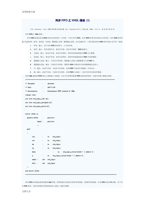
同步FIFO之VHDL描述(1)作者:skycanny时间:2007-09-28 16:09:38 来自:skycanny的笔记浏览次数:1601 文字大小:【大】【中】【小】同步FIFO之VHDL描述同步FIFO的意思是说FIFO的读写时钟是同一个时钟,不同于异步FIFO,异步FIFO的读写时钟是完全异步的。
同步FIFO的对外接口包括时钟,清零,读请求,写请求,数据输入总线,数据输出总线,空以及满信号。
下面分别对同步FIFO的对外接口信号作一描述:1.时钟,输入,用于同步FIFO的读和写,上升沿有效;2.清零,输入,异步清零信号,低电平有效,该信号有效时,FIFO被清空;3.写请求,输入,低电平有效,该信号有效时,表明外部电路请求向FIFO写入数据;4.读请求,输入,低电平有效,该信号有效时,表明外部电路请求从FIFO中读取数据;5.数据输入总线,输入,当写信号有效时,数据输入总线上的数据被写入到FIFO中;6.数据输出总线,输出,当读信号有效时,数据从FIFO中被读出并放到数据输出总线上;7.空,输出,高电平有效,当该信号有效时,表明FIFO中没有任何数据,全部为空;8.满,输出,高电平有效,当该信号有效时,表明FIFO已经满了,没有空间可用来存贮数据。
使用VHDL描述的FIFO将以上面的接口为基础,并且可以参数化配置FIFO的宽度和深度。
先把对外接口描述出来吧。
----------------------------------------------------------------------------------------------------------- Designer : skycanny-- Date : 2007-1-29-- Description : Synchronous FIFO created by VHDLlibrary ieee;use ieee.std_logic_1164.all;use ieee.std_logic_unsigned.all;use ieee.std_logic_arith.all;entity sfifo isgeneric(width : positivedepth : positive);port(clk : in std_logic;rst : in std_logic;wq : in std_logic;rq : in std_logic;data : in std_logic_vector(width - 1 downto 0);q : in std_logic_vector(width - 1 downto 0);empty : out std_logic;full : out std_logic);end entity sfifo;-----------------------------------------------------------------------------------------------------------同步FIFO内部通过控制电路和RAM实现,控制电路主要包括写指针管理电路,读指针管理电路,以及FIFO状态判断电路,对于同步FIFO来讲,读和写的指针管理电路实际上就是二进制计数器。
ALTERA的FIFO的读写控制

ALTERA的FIFO的读写控制为了防止数据堵塞在FIFO里,所以不使用FIFO的almost empty和almost full来控制避免对满FIFO的写以及对空FIFO的读。
假如简单的使用FULL信号来控制FIFO的写,那么就会出现如图1所示的对满FIFO 的写操作,这样就会丢失一个数据。
图1 错误控制FIFO写,导致对已满的FIFO进行误写操作上述FIFO写控制如下:if cnt(5)='1' and fifo_lv1_a_full_sig='0' thenfifo_lv1_a_wrreq_sig <= '1';fifo_lv1_a_data_sig <= cnt(6 downto 0);else fifo_lv1_a_wrreq_sig <= '0';end if;如果改成如下:if cnt(5)='1' and fifo_lv1_a_full_sig='0' and fifo_lv1_a_usedw_sig<15 thenfifo_lv1_a_wrreq_sig <= '1';fifo_lv1_a_data_sig <= cnt(6 downto 0);else fifo_lv1_a_wrreq_sig <= '0';end if;经过上述修改后(注意本例中的FIFO深度是16),当FIFO满了以后,逻辑会及时控制不往已经满了的FIFO里再写入数据了,效果如图2所示:图2 正确控制FIFO写,避免对满FIFO进行误写这种简单通过full信号控制fifo的写,如果不是连续写FIFO一般不会出问题,一旦需要连续的往FIFO 里压入数据,那么当FIFO压满之后FIFO将full信号置位,但是这个动作不会立即通知到user,所以user 会在不知情的情况下又往满的FIFO进行一次写的操作。
同步FIFO之VHDL描述
同步FIFO之VHDL描述(1)作者:skycanny时间:2007-09-28 16:09:38 来自:skycanny的笔记浏览次数:1601 文字大小:【大】【中】【小】同步FIFO之VHDL描述同步FIFO的意思是说FIFO的读写时钟是同一个时钟,不同于异步FIFO,异步FIFO的读写时钟是完全异步的。
同步FIFO的对外接口包括时钟,清零,读请求,写请求,数据输入总线,数据输出总线,空以及满信号。
下面分别对同步FIFO的对外接口信号作一描述:1.时钟,输入,用于同步FIFO的读和写,上升沿有效;2.清零,输入,异步清零信号,低电平有效,该信号有效时,FIFO被清空;3.写请求,输入,低电平有效,该信号有效时,表明外部电路请求向FIFO写入数据;4.读请求,输入,低电平有效,该信号有效时,表明外部电路请求从FIFO中读取数据;5.数据输入总线,输入,当写信号有效时,数据输入总线上的数据被写入到FIFO中;6.数据输出总线,输出,当读信号有效时,数据从FIFO中被读出并放到数据输出总线上;7.空,输出,高电平有效,当该信号有效时,表明FIFO中没有任何数据,全部为空;8.满,输出,高电平有效,当该信号有效时,表明FIFO已经满了,没有空间可用来存贮数据。
使用VHDL描述的FIFO将以上面的接口为基础,并且可以参数化配置FIFO的宽度和深度。
先把对外接口描述出来吧。
----------------------------------------------------------------------------------------------------------- Designer : skycanny-- Date : 2007-1-29-- Description : Synchronous FIFO created by VHDLlibrary ieee;use ieee.std_logic_1164.all;use ieee.std_logic_unsigned.all;use ieee.std_logic_arith.all;entity sfifo isgeneric(width : positivedepth : positive);port(clk : in std_logic;rst : in std_logic;wq : in std_logic;rq : in std_logic;data : in std_logic_vector(width - 1 downto 0);q : in std_logic_vector(width - 1 downto 0);empty : out std_logic;full : out std_logic);end entity sfifo;-----------------------------------------------------------------------------------------------------------同步FIFO内部通过控制电路和RAM实现,控制电路主要包括写指针管理电路,读指针管理电路,以及FIFO状态判断电路,对于同步FIFO来讲,读和写的指针管理电路实际上就是二进制计数器。
fpga中异步信号处理

fpga中异步信号处理
在FPGA中进行异步信号处理是一项重要的任务,因为许多
输入信号可能以不同的时钟信号、频率或相位到达FPGA。
处
理这些异步信号需要特殊的技术和电路设计。
以下是一些常用的异步信号处理方法:
1. 异步复位器:在FPGA中,可以使用异步复位器来处理异
步复位信号。
异步复位器可确保在输入复位信号到达时立即将FPGA重置为初始状态,而不需要等待时钟信号。
2. 异步触发器:通过使用异步触发器,可以将异步输入信号转换为同步的信号。
异步触发器具有单独的时钟信号和数据输入,当触发信号到达时,会将数据输入传递到输出。
这样,异步信号就可以与FPGA中的同步逻辑一起使用。
3. FIFO缓冲器:FIFO(First-In-First-Out)缓冲器用于将异步
信号转换为同步信号,并进行缓冲。
当异步输入信号到达时,它会存储在FIFO中,然后由同步时钟信号按顺序输出。
这样
可以确保异步信号按照正确的顺序被处理。
4. 时序分析和约束:在设计FPGA中的异步信号处理电路时,需要进行时序分析和约束。
时序分析可以帮助确定异步信号到达的时机、时钟边沿等。
时序约束可以确保异步信号处理电路能够按照预期的时序工作。
需要注意的是,异步信号处理在FPGA设计中需要特别小心,
因为异步信号可能导致不稳定的或不确定的行为。
因此,正确设计和验证异步信号处理电路是至关重要的。
异步FIFO

•什么是FIFO随着IC的发展,模块与模块之间的通信设计中,多时钟的情况已经不可避免;数据在不同时钟域之间的传输很容易引起亚稳态;异步FIFO就是一种简单、快捷的解决方案。
FIFO的英文名称是first in first out,是一种先进先出的储存结构;他与普通存储器的区别是没有外部读写地址线,这样使用起来非常简单,但缺点就是只能顺序写入数据,顺序的读出数据,其数据地址由内部读写指针自动加1完成,不能像普通存储器那样可以由地址线决定读取或写入某个指定的地址。
•异步FIFO的结构•异步FIFO的设计难点1.亚稳态的消除;2.空满状态的判断;•什么是亚稳态每一种触发器都会有时序的要求,对于使用上升沿触发的DFF,建立时间(setup time)是时钟上升沿到来之前,数据需要保持稳定的最小时间;保持时间(hold time)是时钟上升沿到来之后,数据需要保持稳定的最小时间;如果setup time或者hold time不满足要求,那么就会导致输出数据的不稳定,引起亚稳态。
•异步FIFO的亚稳态1.由于异步FIFO是工作在两个不同的时钟域中,如果读地址在某一时刻从0111->1000转变;恰好写时钟要在这时刻采样读地址,那么得到的值有可能是0000~1111中的任一个值;这个不确定的读地址值会导致空满状态判断错误。
上面所说的情况,亚稳态的出现是不可避免的;如果把二进制地址计数器转换成格雷码然后再采样,而不是直接采样二进制计数器出来的值,那么就能很好的减少亚稳态的发生;格雷码的特点:1.格雷码相邻的2个数值之间只会有一位发生变化,其余各位都相同;2.格雷码是一种循环码,0和最大数(2的n次方减1)之间也只有一位不同。
引用格雷码之后,相邻数值只有1位发生翻转,1位翻转所引起的亚稳态的概率远远要小于几位同时翻转所引起的概率;因此,格雷码能很好的亚稳态出现的概率。
数值二进制码格雷码0000000 1001001 2010011 3011010 4100110 5101111 6110101 71111001.二进制码转化为格雷码:从最右边第一位开始,依次将每一位与左邻一位异或(XOR),作为对应格雷码该位的值,最左边一位不变;2.格雷码转化为二进制码:从左边第二位起,将每位与左边一位解码后的值异或(XOR),作为该位解码后的值(最左边一位依然不变)。
Altera提供的FIFO说明书
101 Innovation Drive San Jose, CA 95134(408) 544-7000Single- and Dual-Clock FIFO MegafunctionUser GuideQuartus II Version:7.1Document Version: 4.0 Document Date:May 2007Copyright © 2007 Altera Corporation. All rights reserved. Altera, The Programmable Solutions Company, the stylized Altera logo, specific device des-ignations, and all other words and logos that are identified as trademarks and/or service marks are, unless noted otherwise, the trademarks and service marks of Altera Corporation in the U.S. and other countries. All other product or service names are the property of their respective holders. Al-tera products are protected under numerous U.S. and foreign patents and pending applications, maskwork rights, and copyrights. Altera warrants performance of its semiconductor products to current specifications in accordance with Altera's standard warranty, but reserves the right to make changes to any products and services at any time without notice. Altera assumes no responsibility or liability arising out of the ap-plication or use of any information, product, or service described herein except as expressly agreed to in writing by AlteraCorporation. Altera customers are advised to obtain the latest version of device specifications before relying on any published in-formation and before placing orders for products or services.UG-MFNALT_FIFO-4.0ContentsAbout this User GuideRevision History (v)Referenced Documents (v)How to Contact Altera (vi)Typographic Conventions (vi)Chapter 1. About These MegafunctionsDevice Family Support.........................................................................................................................1–1 Introduction............................................................................................................................................1–1 Features...................................................................................................................................................1–2 General Description...............................................................................................................................1–3 The scfifo Megafunction..................................................................................................................1–3 The dcfifo Megafunction.................................................................................................................1–4 Flag Latency in the dcfifo Megafunction......................................................................................1–7 Resource Utilization and Performance.........................................................................................1–8 Chapter 2. Getting StartedSoftware and System Requirements...................................................................................................2–1 Mega Wizard Plug-In Manager Customization................................................................................2–1 FIFO MegaWizard Page Descriptions................................................................................................2–2 Inferring Megafunctions from HDL Code.......................................................................................2–11 Instantiating Megafunctions in HDL Code or Schematic Designs...............................................2–11 Generating a Netlist for EDA Tool Use.......................................................................................2–12 Using the Port and Parameter Definitions..................................................................................2–12 Identifying a Megafunction after Compilation...............................................................................2–13 Simulation.............................................................................................................................................2–13 Quartus II Simulation....................................................................................................................2–13 EDA Simulation..............................................................................................................................2–14 SignalTap II Embedded Logic Analyzer..........................................................................................2–14 Design Examples for the FIFO Megafunctions...............................................................................2–14 Design Files.....................................................................................................................................2–14 Run Functional Simulation...........................................................................................................2–15 Example 1: scfifo Megafunction Behavior in Legacy Mode.....................................................2–16 Initial Write Operation to an Empty Single-Clock FIFO (Legacy Mode):Simulation Results (0 ns to 90 ns)...........................................................................................2–17 Asynchronous and Synchronous Clear Operations in a Single-Clock FIFO (Legacy mode): Simulation Results (90 ns to 190 ns).......................................................................................2–17 Read and Write Operations to an Almost Full Single-Clock FIFO (Legacy Mode):Simulation Results (290 ns to 410 ns).....................................................................................2–18 Read Operation to an Almost Empty Single-Clock FIFO (Legacy Mode):Simulation Results (440 ns to 560 ns).....................................................................................2–19ContentsExample 2: scfifo Megafunction Behavior in Show-Ahead Mode..........................................2–20 Initial Write Operation to an Empty Single-Clock FIFO (Show-Ahead Mode):Simulation Results (0 ns to 90 ns)...........................................................................................2–21 Asynchronous and Synchronous Clear Operations in Single-Clock FIFO (Show-AheadMode): Simulation Results (90 ns to 190 ns).........................................................................2–22 Read and Write Operations to an Almost Full Single-Clock FIFO (Show-Ahead Mode):Simulation Results (290 ns to 410 ns).....................................................................................2–23 Read Operation to an Almost Empty Single-Clock FIFO (Show-Ahead Mode):Simulation Results (440 ns to 560 ns).....................................................................................2–23 Example 3: dcfifo Megafunction Behavior in Legacy Mode....................................................2–24 Initial Write Operation to an Empty Dual-Clock FIFO (Legacy Mode):Simulation Results (0 ns to 150 ns).........................................................................................2–24 Read and Write Operations to an Almost Full Dual-Clock FIFO (Legacy Mode):Simulation Results (280 ns to 400 ns).....................................................................................2–25 Read Operation to an Almost Empty Dual-Clock FIFO (Legacy Mode):Simulation Results (470 ns to 570 ns).....................................................................................2–26 wrempty, rdempty, rdusedw[] and wrusedw[] Behaviors in a Dual-Clock FIFO (LegacyMode) When rdclk is Faster Than wrclk: Simulation Results (580 ns to 680 ns).............2–27 Example 4: dcfifo Megafunction Behavior in Show-Ahead Mode..........................................2–29 Initial Write Operation to an Empty Dual-Clock FIFO (Show-Ahead Mode):Simulation Results (0 ns to 150 ns).........................................................................................2–29 Read and Write Operations to an Almost Full Dual-Clock FIFO (Show-Ahead Mode):Simulation Results (280 ns to 400 ns).....................................................................................2–30 Read Operation to an Almost Empty Dual-Clock FIFO (Show-Ahead Mode):Simulation Results (470 ns to 570 ns).....................................................................................2–31 Example 5: dcfifo Megafunction Behaviorwith Wide Write Data and Narrow Read Output.....................................................................2–32 Example 6: dcfifo Megafunction Behaviorwith Narrow Write Data and Wide Read Output.....................................................................2–34 Chapter 3. SpecificationsSpecifications for the scfifo Megafunction.........................................................................................3–1 Design Requirements for the scfifo Megafunction......................................................................3–1 SCFIFO Ports and Parameters........................................................................................................3–2 Flag Latency in the scfifo Megafunction.......................................................................................3–6 Specifications for the dcfifo Megafunction........................................................................................3–7 Design Requirements for the dcfifo Megafunction.....................................................................3–7 DCFIFO Ports and Parameters.......................................................................................................3–9 Flag Latency in the dcfifo Megafunction....................................................................................3–15About this User Guide Revision History The following table shows the revision history for this user guide.ReferencedDocumentsThis user guide references the following documents:■AN42:Metastability in Altera Devices■Recommended HDL Coding Styles chapter in volume 1 of the Quartus IIHandbook■Synthesis section in volume 1 of the Quartus II Handbook■Quartus II Integrated Synthesis chapter in volume 1 of the Quartus IIHandbook■Design Debugging Using the SignalTap II Embedded Logic Analyzerchapter in volume 3 of the Quartus II Handbook.Date andDocumentVersionChanges Made Summary of ChangesMay 2007v4.0Updates for Quartus II v7.1:●Added support for Arria GX devices.●Updated for new GUI.●Added six design examples in place of functionaldescription.●Reorganized and updated Chapter3,Specifications to have separate tables for thescfifo and dcfifo megafunctions.●Added Referenced Documents section.Major updates for Quartus II v7.1,including addition of six new designexamples in place of the previousfunctional description, and a majorreorganization of Chapter 3 topresent specifications for the scfifoand the dcfifo megafunctionsseparately.March 2007v3.3Updates for Quartus II v7.0:●Minor content changes, including addingStratix®III and Cyclone®III information●Re-took screenshots for software version 7.0Minor updates for Quartus II v7.0,including addition of Stratix III andCyclone IIISeptember 2005v3.2Minor content changes.How to Contact AlteraHow to Contact Altera For the most up-to-date information about Altera® products, refer to the following table.Typographic Conventions This document uses the typographic conventions shown in the following table.Information Type Contact (1)T echnical support /mysupport/T echnical training /training/custrain@Product literature /literature/Altera literature services literature@FTP site Note to table:(1)You can also contact your local Altera sales office or sales representative.Visual Cue MeaningBold Type with Initial Capital Letters Command names, dialog box titles, checkbox options, and dialog box options are shown in bold, initial capital letters. Example: Save As dialog box.bold type External timing parameters, directory names, project names, disk drive names,filenames, filename extensions, and software utility names are shown in boldtype. Examples: f MAX, \qdesigns directory, d: drive, chiptrip.gdf file.Italic Type with Initial Capital Letters Document titles are shown in italic type with initial capital letters. Example: AN 75: High-Speed Board Design.Italic type Internal timing parameters and variables are shown in italic type.Examples: t PIA, n + 1.Variable names are enclosed in angle brackets (< >) and shown in italic type.Example: <file name>, <project name>.pof file.Initial Capital Letters Keyboard keys and menu names are shown with initial capital letters. Examples:Delete key, the Options menu.“Subheading Title”References to sections within a document and titles of on-line help topics areshown in quotation marks. Example: “T ypographic Conventions.”Courier type Signal and port names are shown in lowercase Courier type. Examples: data1,tdi, input. Active-low signals are denoted by suffix n, e.g., resetn.Anything that must be typed exactly as it appears is shown in Courier type. Forexample: c:\qdesigns\tutorial\chiptrip.gdf. Also, sections of anactual file, such as a Report File, references to parts of files (e.g., the AHDLkeyword SUBDESIGN), as well as logic function names (e.g., TRI) are shown inCourier.About this User Guide1.,2.,3., anda.,b.,c., etc.Numbered steps are used in a list of items when the sequence of the items is important, such as the steps listed in a procedure.■●•Bullets are used in a list of items when the sequence of the items is not important. v The checkmark indicates a procedure that consists of one step only.1The hand points to information that requires special attention.c A caution calls attention to a condition or possible situation that can damage ordestroy the product or the user’s work.w A warning calls attention to a condition or possible situation that can cause injuryto the user.r The angled arrow indicates you should press the Enter key.f The feet direct you to more information on a particular topic.Visual Cue MeaningTypographic ConventionsChapter 1.About TheseMegafunctionsDevice Family SupportThe Single-Clock FIFO (scfifo) and Dual-Clock FIFO (dcfifo)megafunctions support the following target Altera ® device families:■Arria™GX ■Stratix ®III ■Stratix II ■Stratix II GX ■Stratix ■Stratix GX ■Cyclone ®III ■Cyclone II ■Cyclone■HardCopy ® II ■HardCopy Stratix ■MAX ® II■MAX 7000AE ■MAX 7000B ■MAX 7000S ■MAX 3000A ■ACEX 1K ®■APEX™ II ■APEX 20KC ■APEX 20KE ■FLEX 10K ®■FLEX ® 10KA ■FLEX 10KE ■FLEX 6000IntroductionAs design complexities increase, use of vendor-specific IP blocks has become a common design methodology. Altera provides parameterizable megafunctions that are optimized for Altera device architectures. Using megafunctions instead of coding your own logic saves valuable design time. Additionally, the Altera-provided functions may offer more efficient logic synthesis and device implementation. You can scale a megafunction’s implementation size by simply setting parameters.FeaturesTo help you efficiently implement FIFOs in your design, the Quartus IIsoftware provides a FIFO MegaWizard® Plug-In Manager that supportsboth the scfifo and the dcfifo megafunctions. The FIFO MegaWizardPlug-In Manager is a user-view wizard that selects and customizes themegafunction based on the properties you select.If the FIFO’s read and write operations use the same clock, the Plug-InManager customizes the scfifo megafunction. If the FIFO’s read and writeoperations use different clocks, the Plug-In Manager customizes thedcfifo megafunction.Features Table1–1 shows the features of the scfifo and dcfifo megafunctions.Table1–1.scfifo and dcfifo Megafunction Features(Part 1 of2) (1)Features DescriptionSupport most of the common FIFO status flags The following status flags are supported:●full●empty●almost_empty (scfifo only)●almost_full (scfifo only)●usedw[] (scfifo only)●wrusedw[] (dcfifo only)●rdusedw[] (dcfifo only)Support different write input data width and read outputdata widthOnly applicable to dcfifoSupport legacy mode Legacy synchronous FIFO mode treats the signal as aread-request signal: the FIFO outputs the data uponassertion of rdreq.Support show-ahead mode Show-ahead synchronous FIFO mode treats therdreq signal as a read-acknowledge signal tominimize the FIFO's read latency. The FIFO outputsdata when it is available; assertion of rdreqacknowledges the data and causes the FIFO to outputthe next data word if available).Support optimization for speed or area Optimizing for speed produces a faster FIFO.Optimizing for area results in fewer resources beingused.Support circuitry protection for FIFO overflow and underflow Overflow checking disables write access while the FIFO is full. Underflow checking disables read access while the FIFO is empty. T urning on both these features prevents FIFO data corruption.About These MegafunctionsGeneral Description The Altera parameterizable scfifo and dcfifo megafunctions can be customized to meet a wide range of data-buffering requirements. For example, the scfifo megafunction is a simple function that can simultaneously read and write in the same clock cycle. The dcfifo megafunction provides data buffering for both synchronousclock-domain and asynchronous clock-domain applications (high-speed data buffering). The dcfifo megafunction also supports simultaneous read and write operations.You can parameterize the scfifo or dcfifo megafunctions to implement almost any combination of width and depth. The FIFO depth must be a power of two, but its only other limitation is the available memory space in the device itself. If the desired combination is not available on the Plug-In Manager menu, simply enter the width and depth required for your design. You can also configure the scfifo and dcfifo megafunctions to output several optional FIFO flag signals, including empty and full flags and the number of words read or written.For a more detailed specification and requirements description for the scfifo and dcfifo megafunctions, refer to the “Design Requirements for the scfifo Megafunction” and “Design Requirements for the dcfifo Megafunction” sections in Chapter3, Specifications.The scfifo MegafunctionThe scfifo megafunction uses a single clock signal for FIFO read and write operations, and allows simultaneous read and write transactions.The scfifo megafunction provides two operational modes:■Legacy synchronous FIFO mode (Legacy mode)■Show-ahead synchronous FIFO mode (Show-ahead mode)Support simultaneous read and write Read and write operations can occur simultaneously.Support additional bit as MSB extension of usedw[] ports An additional bit becomes the MSB for the usedw[] port, allowing it to hold the correct count when the FIFO is full instead of the value 0. This feature is available for the dcfifo megafunction in the Arria GX, Stratix III, Stratix II, Stratix II GX, Cyclone III, and Cyclone II device families.Note to Table1–1:(1)Refer to the “SCFIFO Ports and Parameters” and “DCFIFO Ports and Parameters” sections in Chapter3,Specifications for more detailed descriptions of these features.Table1–1.scfifo and dcfifo Megafunction Features(Part 2 of2) (1)Altera Corporation 1–3General DescriptionWhen the scfifo megafunction is configured in Legacy mode, read data isavailable on the first clock cycle after rdreq is asserted (that is, the rdreqsignal operates as a normal read request). However, when the scfifomegafunction is configured in Show-ahead mode, the rdreq signaloperates as a read-acknowledge signal. Thus, the first word of valid datain the FIFO appears on its outputs without a read operation occurring.The almost_full and almost_empty output ports are optional andare only available in scfifo. These flags provide an early indication thatthe FIFO is almost full or almost empty.The value on usedw[] increments for every write operation anddecrements for every read operation. The full signal is asserted on therising clock edge at which usedw[] reaches the maximum number ofwords the FIFO can store, while the empty signal is asserted on the risingclock edge at which usedw[] reaches its minimum value of zero.For a more detailed description of these ports, refer to the “SCFIFO Portsand Parameters” section in Chapter3, Specifications.The dcfifo MegafunctionThe dcfifo megafunction is well-suited for the complex data processingrequirements of high-data-rate, asynchronous-clock-domainapplications, in which data is transferred or buffered betweenasynchronous clock domains. This megafunction can also performsimultaneous read and write transactions. The dcfifo megafunction is adual-pipelined function that stores data in the dual-port memorystructures available in Altera devices.Like the scfifo megafunction, the dcfifo megafunction provides twooperational modes:■Legacy synchronous FIFO mode (Legacy mode)■Show-ahead synchronous FIFO mode (Show-ahead mode)When the dcfifo megafunction is configured in Legacy mode, read data isavailable on the first clock cycle after rdreq is asserted (that is, the rdreqsignal operates as a normal read request). However, when the dcfifomegafunction is configured in Show-ahead mode, the rdreq signaloperates as a read-acknowledge signal. Thus, the first word of valid datain the FIFO appears on its outputs without a read operation occurring.1–4Altera CorporationAbout These MegafunctionsYou can configure the dcfifo megafunction to output any of the followingsix FIFO status flags:■The wrusedw[]and rdusedw[]signals, which represent thenumber of words stored in the FIFO. The wrusedw[]signal is aregistered output that is synchronous with the write clock (wrclk),and the rdusedw[]signal is a registered output that is synchronouswith the read clock (rdclk).■The rdfull and rdempty signals, which indicate whether the FIFOis full or empty. These signals are registered outputs synchronouswith the read clock.■The wrfull and wrempty signals, which indicate whether the FIFOis full or empty. These signals are registered outputs synchronouswith the write clock.Figure1–1 is a block diagram that shows how the dcfifo megafunction isimplemented with an Altera Memory Block. All control logic isimplemented in logic elements (LEs).Altera Corporation 1–5General DescriptionFigure1–1.DCFIFO Megafunction Block DiagramFigure1–1 shows the dcfifo megafunction uses two independent clocks,wrclk and rdclk. The wrclk synchronizes data write transactions tothe Altera Memory Block at the memory location indicated by the WriteAddress Pointer. The rdclk synchronizes data read transactionsfrom the Altera Memory Block from the memory location indicated by theRead Address Pointer. The Flag Control Logic generates the six FIFOstatus flags by subtracting the value of the Read Address Pointerfrom the value of the Write Address Pointer.Because the Read Address Pointer and the Write AddressPointer are in different clock domains, unsynchronized values outputon the FIFO status flag signals can be incorrect as a result of metastability,especially when the read and write clock domains are not related.Synchronization in the Read Pipeline eliminates the effects of this1–6Altera CorporationAbout These Megafunctionsmetastability in the paths from the Read Address Pointer to the FlagControl Logic. Similarly, synchronization in the Write Pipeline eliminatesthe effects of this metastability in the paths from the Write AddressPointer to the Flag Control Logic. The register delays in the pipelinesdelay the effects of updates to the two pointers on the FIFO status flags.Therefore, these synchronization pipelines cause the FIFO status signalsrdempty, rdfull, rdusedw[], wrempty, wrfull, and wrusedw[] tobe delayed by multiple clock cycles.f For more information about synchronization pipelines, refer toAN42:Metastability in Altera Devices.Flag Latency in the dcfifo MegafunctionThe Read Pipeline and the Write Pipeline shown in Figure1–1 cause theFIFO status flag output signals to be delayed by multiple clock cycles. Therdfull,rdempty, wrfull, and wrempty flags are generated fromdirect internal counter comparisons, and have lower latencies than therdusedw[] and wrusedw[] signals. This section explains how therdusedw[] and wrusedw[] signals are generated and how theycontribute to the pipeline latency.The value on the wrusedw[] signal is calculated in the wrclk clockdomain. The Read Address Pointer value is passed from the rdclkclock domain into the Flag Control Logic and is compared with theWrite Address Pointer value in the wrclk clock domain. The FlagControl Logic calculates the value on the wrusedw[] signal bysubtracting the Read Address Pointer value from the current WriteAddress Pointer value. However, the Read Address Pointercannot be passed to the Flag Status Logic directly because the ReadAddress Pointer value may be changing during the calculation.Instead, the Read Address Pointer value is Gray-code encoded priorto the calculation. This encoding ensures only one bit changes at once. Ifthe Flag Status Logic uses the encoded Read Address Pointer value whileit is changing, the value used is either the old address or the new address,and not an intermediate, irrelevant value. However, two issues remain:■If multiple registers use the changing bit as input, some registers maycapture a zero and others a one, leading to an inconsistency in thelogic calculations.■If the setup or hold time of the changing bit is violated, a register maybe in a metastable state, and may require time to recover.To solve these problems, the encoded Read Address Pointer value issynchronized two or more times with the wrclk clock. Thissynchronization occurs in the Read Pipeline. The Flag Control Logic thenAltera Corporation 1–7General Descriptionconverts the synchronized, encoded Read Address Pointer back intostandard binary format, to enable subtraction, and generates thewrusedw[] flag output signal.The rdusedw[] flag is generated similarly in the rdclk clock domain,requiring synchronization of the Write Address Pointer value in theWrite Pipeline. The encoding and synchronization lead to a delay ofseveral clock cycles to update the rdusedw[]and wrusedw[] flags.Because of this latency, the rdusedw[] and wrusedw[] output signalsare unlikely to have the same value until several clock cycles pass with noread or write transactions.The flag latencies may vary for different configuration settings and indifference device families.For more detailed information about the latency of the dcfifomegafunction FIFO status flag, refer to the “Flag Latency in the dcfifoMegafunction” section in Chapter3, Specifications.Resource Utilization and PerformanceAltera recommends that you implement FIFO functions in the memorystructures of Altera devices. If all the memory resources are used for othermemory functions, the Quartus II software can implement the FIFOs inLEs as well.You may see a significant decrease in performance when thesefunctions are implemented in LEs. Altera recommends you select theAuto option and let the Quartus II program decide on the memoryimplementation.The MegaWizard Plug-In Manager displays the estimated resourceusage. Different megafunction configurations produce different resourceusage counts.1For the scfifo and dcfifo megafunctions, resource usage isreduced when overflow and underflow checking are disabled.1For the dcfifo megafunction, resource usage is further reducedwhen the optional output signals rdusedw[] and wrusedw[]are not selected.1–8Altera Corporation。
异步清零法原理
异步清零法原理
异步清零法是一种用于数字电路中的异步复位技术,用于将电路中的寄存器或触发器的状态清零。
该方法基于电路中逻辑门的特性,实现异步清零功能。
异步清零法的原理是利用与门和非门(反相器)来实现异步复位功能。
异步复位信号通常为一个低电平信号(例如0V),当接收到复位信号时,寄存器或触发器的状态会被强制清零。
以下是异步清零法的一种基本实现方式:
1. 异步复位信号:一个低电平信号(例如0V),表示需要将寄存器或触发器的状态清零。
2. 与门(AND gate):将异步复位信号和需要清零的寄存器或触发器的时钟信号作为输入,输出连接到寄存器或触发器的清零端(例如CLR端)。
3. 非门(NOT gate):将异步复位信号作为输入,输出连接到与门的另一输入端,将异步复位信号进行取反(反相)。
当异步复位信号为低电平时(0V),与门的输入为低电平与时钟信号,输出为低电平,对应于清零端(CLR端)的激活信号。
寄存器或触发器的状态被强制清零。
当异步复位信号为高电平时,与门的输入为高电平与时钟信号,输出为高电平,不会对寄存器或触发器的状态造成影响。
异步清零法可以确保在任何情况下都能及时清零寄存器或触发器,即使其他电路出现故障或异常情况。
它在数字电路设计中广泛应用,可以实现稳定和可靠的复位功能。
关于ALTERA提供的FIFO核使用原理 改
关于ALTERA提供的FIFO核使用原理ALTERA提供了LPM_FIFO参数宏模块,可以在代码中例化使用。
FIFO有两种工作模式:(1)SCFIFO,(2)DCFIFO其中SCFIFO指读写用一个时钟进行同步,可以支持同时读写的功能。
其中DCFIFO指读写使用不同的时钟进行同步,这在设计多时钟系统中相当有用,可用于不同时钟同步信号之间的同步调整。
首先看看DCFIFO模式下的几个比较重要的信号:[A]在写端,主要有以下几个信号:(1) data[n-1:0]:写入数据信号总线;(2) wrreq:写入请求信号,高有效(2) wrclk:写入同步时钟;(3) wrfull, wrempty:用于指示写端FIFO为空或者满的状态;(4) wrusedw[log2(SIZE_FIFO)-1:0] :写入的数据个数,按写入个数递增;上述信号都与写入时钟srclk同步;[B]在读端,主要有以下几个信号:(1) q[n-1:0]:读取数据信号总线;(2) rdreq:读取请求/确认信号,高有效(2) rdclk:读取同步时钟;(3) rdfull, rdempty:用于指示读端FIFO为空或者满的状态;(4) rdusedw[log2(SIZE_FIFO)-1:0] :读取FIFO主要有两种工作模式:(1) Legacy mode(Legacy synchronous FIFO mode )(2) Show-ahead mode(Show-ahead synchronous FIFO mode)其中:在Legacy mode,读端的rdreq信号作为读取FIFO的请求信号(REQ),读取数据在rdreq置位后的第二个时钟周期有效。
在Show-ahead mode,读端的rdreq信号作为读取FIFO的确认信号(ACK),读取数据在rdreq置位后立即有效,不要额外的读取周期。
下面分别给出Legacy mode和Show-ahead mode的读写时序:[A] Legacy mode[B] Show-ahead mode由上述时序可以看出两种模式的区别。
怎么用Verilog语言描述同步FIFO和异步FIFO
怎么⽤Verilog语⾔描述同步FIFO和异步FIFO感谢知乎龚⼤佬打杂⼤佬⽹上⼏个nice的博客(忘了是哪个了。
)前⾔虽然FIFO都有IP可以使⽤,但理解原理还是⾃⼰写⼀个来得透彻。
什么是FIFO?Fist in first out。
先⼊先出的数据缓存器,没有外部读写地址线,可同时读写。
规则:永远不要写⼀个已经写满了的fifo。
永远不要读⼀个读空了的fifo。
FIFO种类?同步FIFO和异步FIFO。
同步FIFO只有⼀个时钟,也就是说写端和读端的时钟是⼀⽑⼀样的。
异步FIFO读端和写端两个时钟则是不⼀样的。
包括同频异相,异频异相。
FIFO⽤途?1. 数据缓冲器。
⽐如你写端burst⼀个数据,没有fifo缓冲的话就炸了。
Fifo会把写端的突发数据吃到肚⼦⾥,读端可以慢慢的⼀个个读出来。
2. 跨时钟域。
异步fifo主要使⽤在不同时钟域的边缘,⽤来同步数据到另⼀个时钟域。
3.ALTERA FIFO IP 的缺点是什么?虽然altera贴⼼的提供了FIFO的IP块,但是对于可移植性与⾃定义位宽深度更好的话,还是⾃⼰写的更佳。
FIFO深度如何计算?(避免溢出)对于异步fifo,如果读时钟⼤于写时钟且每个周期读写,那么⼀定是会读空的,反之⼀定会被写满。
⼀般来说,不会设计这么⽆聊的东西。
假设写端有突发的数据,⽽读端是均匀的读出,怎么保证fifo不溢出呢?异步FIFO快转慢的问题:可能采样踩不到某些值。
同步FIFO:当缓冲器使⽤,可以⽤ram资源搭。
原理图:信号定义:clk:时钟信号rst_n:异步复位信号wr:写请求rd:读请求data:数据输⼊q:数据输出full:满信号,表⽰fifo吃饱了empty:空信号,表⽰fifo肚⼦已经空掉了usedw:表⽰fifo中已有的数据个数仿真:没有usedw款:有usedw款:资源使⽤量:如何设计⼀个异步FIFO?⼀般⽤作跨时钟域,可⽤ram搭。
判断读空与写满,读写指针要跨时钟域,所以采⽤格雷码减少亚稳态。
- 1、下载文档前请自行甄别文档内容的完整性,平台不提供额外的编辑、内容补充、找答案等附加服务。
- 2、"仅部分预览"的文档,不可在线预览部分如存在完整性等问题,可反馈申请退款(可完整预览的文档不适用该条件!)。
- 3、如文档侵犯您的权益,请联系客服反馈,我们会尽快为您处理(人工客服工作时间:9:00-18:30)。
altera fifo异步清零信号的时序
一、引言
在数字电路设计中,FIFO(First In First Out)是一种常见的数据缓冲器,用于解决不同速度的数据传输之间的数据流失问题。
Altera是一家知名的FPGA芯片制造商,其FIFO模块提供了异步清零信号来实现清空缓冲区的功能。
二、FIFO异步清零信号的定义
FIFO异步清零信号是一种特殊的控制信号,用于将FIFO缓冲区中的数据全部清空。
当该信号被激活时,FIFO模块会将缓冲区中的数据全部丢弃,并将指针重置为初始状态。
三、FIFO异步清零信号的工作原理
FIFO异步清零信号的工作原理如下:
1. 当FIFO异步清零信号被激活时,FIFO模块会检测到该信号的变化。
2. FIFO模块会立即停止写入数据和读取数据的操作,并将指针重置为初始状态。
3. FIFO模块会将缓冲区中的数据全部丢弃,不再进行任何处理。
4. FIFO异步清零信号被取消激活后,FIFO模块会恢复正常的读写操作。
四、FIFO异步清零信号的时序特性
FIFO异步清零信号的时序特性如下:
1. 异步清零信号可以随时激活,无需与其他信号同步。
2. 异步清零信号的激活时间和激活持续时间可以根据设计要求进行调整。
3. FIFO模块在接收到异步清零信号后会立即响应,无需等待时钟信号。
4. 异步清零信号的取消激活时间可以根据设计要求进行调整。
5. 异步清零信号的取消激活时间应保证足够长,以确保FIFO模块完全恢复正常操作。
五、FIFO异步清零信号的注意事项
在使用FIFO异步清零信号时,需要注意以下几点:
1. 异步清零信号的激活和取消激活应遵循设计规范,不得出现脉冲信号或持续激活导致异常操作。
2. 异步清零信号的激活和取消激活时间应考虑到FIFO模块的响应时间和恢复时间,避免信号过短或过长导致操作不稳定。
3. 在设计中,应考虑到异步清零信号与其他控制信号的相互作用,避免冲突或误操作。
六、总结
FIFO异步清零信号是一种重要的控制信号,用于清空FIFO缓冲区中的数据。
了解其工作原理和时序特性对于正确使用和设计FIFO模块至关重要。
在实际应用中,我们应根据具体需求合理配置异步清
零信号的激活和取消激活时间,以确保FIFO模块的正常操作和数据流动。
七、参考资料
[1] Altera Corporation. "FIFO Intel FPGA IP User Guide." Altera Corporation, 2019.。