贴片开关二极管 MMBD4148TW SOT-363 规格书推荐
贴片二极管型号、参数

相关型号
IS2836 IS2838 ISS223
ISS221
ISS123
Vr Min Vde
IF mA
VF
Vde
Min
IF mA
Ir
Max uA
VR
Trr ns
80 100
300
80
80 100
300
80
80 100
300
80
80 100
300
80
80 100
300
80
80 100
300
80
80 100
70 200
250
70
40 200 1 40
35
70 200 1 15
50
30 200 1 100 2 25
75 200 1 50
75
内部结构 STYLE
12 9
18 8 18 11 18 8 8 8 8 9 9 11 11 9 12 12 89 11 12 89 11 12 89 11 12 8
创作时间:二零二一年六月三十日
Trr (US)
封装方式 NOTE
1
30 1
1
4 SMA(D0214AC)
1
30 1
1
4 SMA(D0214AC)
1
30 1
1
4 SMA(D0214AC)
1
30 1
1
4 SMA(D0214AC)
1
30 1
1
4 SMA(D0214AC)
1
30 1
1
4 SMA(D0214AC)
30 1
20MA 4
D0214
55 55 55
贴片开关二极管型号 MMBD7000LT1G BAS16WT1G BAV99WT1G 贴片低压差稳压器 MC33269DT-3.3G TL431ACLPG

贴片开关二极管型号MMSD4148T1G MMBD7000LT1G BAS16WT1G BAV99WT1G 贴片低压差稳压器MC33269DT-3.3G TL431ACLPG深圳市金色长城科技有限公司是一家集渠道代理与分销的专业化半导体公司,产品信息网络资源丰富,战略合作遍布全球。
主要供应于通讯,电源。
安防,汽车电子,工业控制,物联网,新能源,智能家居,智慧家庭等专业领域,诚实经营,务实进取。
为AI智能世界提供安全互联的解决方案!拥有务实高效的金牌团队及完善的配套服务从而促进了供求关系的平衡,满足了生产厂商的采购需求!金色长城,赢在品牌战略!整合优质资源!形成优势互补!达成财富共享!公司产品品种规格齐全,有普通整流、快速恢复、高效率、超快速和肖特基等各种系列与多种封装形式的二极管。
产品介绍贴片二极管又称晶体二极管,简称二极管(diode),另外,还有早期的真空电子二极管;它是一种具有单向传导电流的电子器件。
在半导体二极管内部有一个PN结两个引线端子,这种电子器件按照外加电压的方向,具备单向电流的转导性。
一般来讲,贴片晶体二极管是一个由p型半导体和n型半导体烧结形成的p-n结界面。
在其界面的两侧形成空间电荷层,构成自建电场。
当外加电压等于零时,由于p-n 结两边载流子的浓度差引起扩散电流和由自建电场引起的漂移电流相等而处于电平衡状态,这也是常态下的二极管特性。
具体参数贴片二极管的管压降:硅二极管(不发光类型)正向管压降0.7V,锗管正向管压降为0.3V,发光二极管正向管压降会随不同发光颜色而不同。
主要有三种颜色,具体压降参考值如下:红色发光二极管的压降为2.0--2.2V,黄色发光二极管的压降为1.8—2.0V,绿色发光二极管的压降为3.0—3.2V,正常发光时的额定电流约为20mA。
贴片二极管的电压与电流不是线性关系,所以在将不同的贴片二极管并联的时候要接相适应的电阻。
贴片二极管特性贴片二极管(英语:Diode),电子元件当中,一种具有两个电极的装置,只允许电流由单一方向流过。
FH1N4148(LL-34-DO-35)贴片式开关二极管规格书

ఎਈऔ!Switching DiodeSwitching Diode ఎਈऔFH1N41481DESCRIPTION & FEATURES 概述及特點Low forward voltage 低正向壓降Fast reverse recovery time 快恢復時間 Ultra High Speed Switching Application 超高速開關應用PIN ASSIGNMENT 引腳說明PIN NUMBER 引腳序號PIN NAME 管腳符號 LL-34/DO-35FUNCTION 功能 A 1 Anode C 2 CathodeLL-34DO-35Maximum Ratings&Thermal Characteristics (T a =25℃) 最大額定值及熱特性CHARACTERISTIC 特性參數 Symbol符號 Value 數值 Unit 單位Maximum Peak Repetitive Reverse Voltage最大反向峰值電壓V RRM 100 V Maximum RMS Voltage 反向電壓V RMS 75 V Voltage Rise when Switching ON Tested with 50mA Forward Pulses Tp=0.1s, Rise Time <30ns, fp=5 to 100KHzV FR 2.5 V Rectifier Current (average) Half Wave Rectification with Resist.Load At T A =25℃ andf ≥50Hz 半波整流電流 I O 150 mA Surge Forward Current at t <1s and T A =25℃I FSM 500 mA Power Dissipation at T A =25℃PTOT 500 mW Thermal Resistance Junction to ambient air 熱阻 R ΘJA0.35℃/mW Junction and Storage Temperature 結溫和儲存溫度T J ,T STG 175,-65~150℃ELECTRICAL CHARACTERISTICS 電特性(T A =25℃ unless otherwise noted 如無特殊說明,溫度為25℃)Characteristic 特性參數Symbol 符號 Test Condition 測試條件 Min 最小值TYPE 典型值 Max 最大值Unit單位Forward Voltage 正向電壓V F I F =10mA — — 1.0 V Reverse Voltage 反向電壓V RI R =100µA 75 — — V V R =20V — — 25 nAV R =75V — — 5 µA Reverse Voltage LeakageCurrent 反向漏電流I RV R =20V, Tj=150℃ — — 50 µATotal Capacitance 電容 C T V R =0,f = 1.0MHz — — 4.0 pF Reverse Recovery Time 反向恢復時間 t rr From IF=10mA toIR=1mA,VR=6V,R=100Ω— — 4 nSRectification Efficiency整流效率ηr f =100MHZ, VRF =2V 0.45 — — —。
LL4148开关二极管规格书
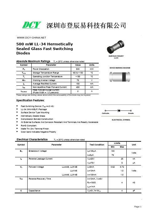
Notes: 1. 2. All dimensions are within DO213AC JEDEC standard. LL-34 polarity denoted by cathode band.
Page 3
These ratings are limiting values above which the serviceability of the diode may be impaired.
Specification Features:
Fast Switching Device (TRR <4.0 nS) LL-34 (Mini-MELF) Package Surface Device Type Mounting Hermetically Sealed Glass Compression Bonded Construction All External Surfaces Are Corrosion Resistant And Terminals Are Readily Solderable RoHS Compliant Matte Tin (Sn) Terminal Finish Color band Indicates Negative Polarity
f = 1MHz Ta = 25℃ 1.0
0.5
0.0 0 5 10 15 20 25 30
VR - Reverse Voltage [V]
Figure 1. Power Dissipation vs Ambient Temperature
Valid provided leads at a distance of 0.8mm from case are kept at ambient temperature
贴片M系列三极管参数
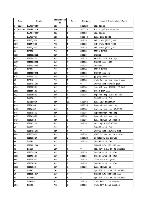
R F XQ XQ W UQ XQ K W W W W W E DN E N W N N M M W W C C C C M A A A A W UQ UQ M W B B B B M U
SOT23 SOT143 SOT143R SOT346 SOT363 SOT346 SOT23 SOT23 SOT323 SOT23 SOT23 SOT323 SOT346 SOT323 SOT346 SOT23 SOT323 SOT346 SOT323 SOT346 SOT143 SOT143R SOT343 SOT23 SOT323 SOT346 SOT323 SOT346 SOT23 -
Code M (blue) M (white) M M M08 M09 M10 M1 M1B M1E M1F M1J M2 M2B M2C M3 M3 M3A M3B M3J M4 M4 M4A M4B M4C M4E M4F M4G M5 M5 M5C M5 M6 M6 M6 M6A M6B M6C M6E M6H M7 M7 M8 M8 M8p
Leaded Equivalent/Data pin diode 5.4-2.3pF varicap in pin diode dual pin diode VHF n-ch JFET J308 VHF n-ch JFET J309 VHF n-ch JFET J310 BFW11 BF245 2N2222 MPSA43 200V Vce npn 2N5550 npn 140V 2N2369A BFW12 BF245 2N2907 pnp gp gp pnp MPSA70 n-ch fet gp low level amp 2N5086 hfe 60-120 pnp npn VHF amp 400MHz fT 30V 2N918 UHF amp pnp VHF amp 2GHz fT 15V 2N4856 n-ch fet dual UHF schottky Hyperabrupt varicap dual cc varicap 45pF/2V Hyperabrupt varicap Hyperabrupt varicap dual MBD101 in series varicap 6.8pF MV2101 2N5457 n-ch fet 2N5086 hfe 135-270 pnp 100V 2x series sw diodes 2x MBD101 in series 2N4858 n-ch fet 2N5086 hfe 200-400 pnp npn 40V 0.1A sw fT 250MHz 2N4416 n-ch rf jfet 2N5484 n-ch rf jfet U310 n-ch rf jfet 2N5460 n-ch rf jfet dual MBD101 cc npn 40V 0.1A sw fT 300MHz 2N5086 hfe 300-600 pnp npn 40V 0.1A sw fT 250MHz n-ch 50V 0.11A mosfet n-ch 50V 0.11A mosfet
MMSD4148 SOD-123 规格书推荐

ns
−
4.0
Product parametric performance is indicated in the Electrical Characteristics for the listed test conditions, unless otherwise noted. Product performance may not be indicated by the Electrical Characteristics if operated under different conditions.
0
2
4
6
8
VR, REVERSE VOLTAGE (VOLTS)
Figure 4. Capacitance
3
CD, DIODE CAPACITANCE (pF)
MMSD4148, SMMSD4148
PACKAGE DIMENSIONS
D
ÂÂÂÂÂÂ1 ÂÂ
HE
E
2
b
SOD−123 CASE 425−04
SOLDERING FOOTPRINT*
0.91
ÉÉÉÉÉÉ 0.036 ÉÉÉÉÉÉ
1.22 0.048
2.36
0.093
4.19
0.165
ǒ Ǔ SCALE 10:1
mm inches
*For additional information on our Pb−Free strategy and soldering details, please download the ON Semiconductor Soldering and Mounting Techniques Reference Manual, SOLDERRM/D.
JCET长电1N4148W高速开关二极管规格书
Capacitance Characteristics
1.6 Ta=25℃ f=1MHz
1.4
1.2
1.0
0.8
0.6
0
4
8
12
16
20
REVERSE VOLTAGE VR (V)
Power Derating Curve
500
400 BAV16W 1N4148W
300
200
100
0
0
25
50
75
100
Email:sales@
1
Limit 100
100
71 300 150 2.0 350 400 250 150 -55~+150
Unit V
V
V mA mA A mW ℃/W ℃ ℃
D,Nov,2017
ELECTRICAL CHARACTERISTICS
VF2
0.855 V
VF3
1.0
V
VF4
1.25
V
IR1
1
μA
IR2
25
nA
CT
2
pF
trr
4
ns
Conditions IF=1mA IF=10mA IF=50mA
IF=150mA VR=75V VR=20V VR=0V,f=1MHz IF=IR=10mA Irr=0.1XIR,RL=100Ω
1.6
FORWARD VOLTAGE VF (V)
REVERSE CURRENT IR (nA)
10000 3000 1000 300 100 30 10 3 1 0
Reverse Characteristics
FOSAN富信电子 二级管 1N4148WS-产品规格书
安徽富信半导体科技有限公司ANHUI FOSAN SEMICONDUCTOR TECHNOLOGY CO.,LTD.1N4148WSSOD-323Switching Diode 开关二极管■Features 特点Fast Switching Speed 快的开关速度Surface mount device 表面贴装器件High Conductance 高电导率Case 封装:SOD-323Marking 印字:T4■Maximum Rating 最大额定值(T A =25℃unless otherwise noted 如无特殊说明,温度为25℃)Characteristic 特性参数Symbol 符号Rating 额定值Unit 单位Non-Repetitive Peak Reverse Voltage 不重复反向峰值电压V RM 100V DC Reverse Voltage 直流反向电压V R 75V Peak Repetitive Reverse Voltage 峰值重复反向电压V RRM 75V Woke Peak Reverse Voltage 峰值反向工作电压V RWM 75V RMS Reverse Voltage 反向电压均方根值V R(RMS)53V Forward Rectified Output Current 正向工作电流I O 200mA Non-Repetitive Peak Surge Current@t=1µS 不重复峰值浪涌电流@t=1S I FSM 21A Power Dissipation 耗散功率P D 200mW Thermal Resistance Junction-Ambient 结到环境热阻R θJA 625℃/W Junction/StorageTemperature 结温/储藏温度T J,T stg-50to+150℃℃■Electrical Characteristics 电特性(T A =25℃unless otherwise noted 如无特殊说明,温度为25℃)Characteristic 特性参数Symbol 符号Min 最小值Max 最大值Unit 单位Condition 条件Reverse Voltage 反向电压V R75VI R =1µA Forward Voltage 正向电压V F 0.7150.8551.01.25V I F =1mA I F =10mA I F =50mA I F =150mA Reverse Current 反向电流I R 125µA nA V R =75V V R =20V Junction Capacitance 结电容C J2pFV R =4V,f=1MHz安徽富信半导体科技有限公司ANHUI FOSAN SEMICONDUCTOR TECHNOLOGY CO.,LTD.1N4148WS ■Typical Characteristic Curve典型特性曲线■Dimension外形封装尺寸。
1N4148WT快速开关二极管SOD-523规格书
200
Power Derating Curve
CAPACITANCE BETWEEN TERMINALS CT (pF)
1.1
(mW) POWER DISSIPATION
5 10 15 20
150
1.0
PD
100 0.9 50 0.8 0 0 0 25 50 75 100 125 150
ELECTRICAL CHARACTERISTICS(Ta=25℃ unless otherwise specified)
Parameter Reverse voltage Reverse current Symbol V(BR) IR IR=1μA VR=75V VR=20V IF=1mA IF=10mA Forward voltage VF IF=50mA IF=150mA Total capacitance Reverse recovery time Ctot trr VR=0V,f=1MHz IF= IR =10mA, Irr=0.1*IR,RL=100Ω Test conditions Min 75 1 25 0.715 0.855 1 1.25 2 4 Typ Max Unit V µA nA V V V V pF ns
1n4148wt快速开关二极管sod523规格书
1N4148WT
FEATURES
FAST SWITCHING DIODE
SOD-523
Small Package Low Reverse Current Fast Switching Speed Surface Mount Package Ideally Suited for Automatic Insertion
MMSD4148T3G;MMSD4148T1G;MMSD4148T1;中文规格书,Datasheet资料
5I M G
(Note: Microdot may be in either location)
ORDERING INFORMATION
Device MMSD4148T1G SMMSD4148T1G MMSD4148T3G SMMSD4148T3G Package SOD−123 (Pb−Free) SOD−123 (Pb−Free) SOD−123 (Pb−Free) SOD−123 (Pb−Free) Shipping† 3,000 / Tape & Reel 3,000 / Tape & Reel 10,000 / Tape & Reel 10,000 / Tape & Reel
ON Semiconductor and are registered trademarks of Semiconductor Components Industries, LLC (SCILLC). SCILLC reserves the right to make changes without further notice to any products herein. SCILLC makes no warranty, representation or guarantee regarding the suitability of its products for any particular purpose, nor does SCILLC assume any liability arising out of the application or use of any product or circuit, and specifically disclaims any and all liability, including without limitation special, consequential or incidental damages. “Typical” parameters which may be provided in SCILLC data sheets and/or specifications can and do vary in different applications and actual performance may vary over time. All operating parameters, including “Typicals” must be validated for each customer application by customer’s technical experts. SCILLC does not convey any license under its patent rights nor the rights of others. SCILLC products are not designed, intended, or authorized for use as components in systems intended for surgical implant into the body, or other applications intended to support or sustain life, or for any other application in which the failure of the SCILLC product could create a situation where personal injury or death may occur. Should Buyer purchase or use SCILLC products for any such unintended or unauthorized application, Buyer shall indemnify and hold SCILLC and its officers, employees, subsidiaries, affiliates, and distributors harmless against all claims, costs, damages, and expenses, and reasonable attorney fees arising out of, directly or indirectly, any claim of personal injury or death associated with such unintended or unauthorized use, even if such claim alleges that SCILLC was negligent regarding the design or manufacture of the part. SCILLC is an Equal Opportunity/Affirmative Action Employer. This literature is subject to all applicable copyright laws and is not for resale in any manner.
- 1、下载文档前请自行甄别文档内容的完整性,平台不提供额外的编辑、内容补充、找答案等附加服务。
- 2、"仅部分预览"的文档,不可在线预览部分如存在完整性等问题,可反馈申请退款(可完整预览的文档不适用该条件!)。
- 3、如文档侵犯您的权益,请联系客服反馈,我们会尽快为您处理(人工客服工作时间:9:00-18:30)。
JIANGSU CHANGJIANG ELECTRONICS TECHNOLOGY CO., LTD
www.cj-elec.com 1
SOT-363 Plastic-Encapsulate Diodes
Maximum Ratings and Electrical Characteristics, Single Diode @T
a=25℃
Parameter Symbol Limit Unit
Non-Repetitive Peak Reverse Voltage
V
RM
100 V
Peak Repetitive Peak
Reverse Voltage
Working Peak Reverse Voltage
DC Blocking Voltage
V
RRM
VRWMVR75
V
RMS Reverse Voltage
V
R(RMS)
53 V
Forward Continuous Current
I
FM
300 mA
Average Rectified Output Current
IO150 mA
I
FSM
2
.0
A
Power Dissipation
Pd 200 mW
Thermal
Resistance Junction
to
Ambient
R
θJA
℃/W
℃
℃
Forward Surge Current @
t=8.3ms
Non-Repetitive Peak
Junction Temperature
Storage Temperature
T
j
150
TSTG-55~+150
625
SOT-363
61524
3
BAS16TW/MMBD4148TW
SWITCHING DIODE
FEATURES
z
Fast Switching Speed
z
For General Purpose Switching Applications
z
High Conductance
Electrical Ratings @Ta=25℃
Parameter Symbol MinTypMaxUnit Conditions
Reverse breakdown voltageV (BR) 75 V IR=10μA
VF1 0.715V IF=1mA
VF2 0.855V IF=10mA
VF3 1.0 V IF=50mA
Forward voltage
VF4 1.25 V I
F
=150mA
IR1 1 μA VR=75V
Reverse current
IR2 25 nA V
R
=20V
Capacitance between terminals
CT 2 pF VR=0V,f=1MHz
Reverse
recovery time
t
rr
4
ns
I
F=IR
=10mA
Irr=0.1XI
R,RL
=100Ω
MARKING:
MMBD4148TW:KA2BAS16TW:KA2
Solid
dot = Green molding compound device,
if none,the normal device.
KA2
+
-
+ +
- -
KA2
+ - + +
- -
KA2
KA2
Solid
dot = Pin1 indicate.
C,Mar,2016
www.cj-elec.com2
Typical Characteristics
0.00.20.40.60.81.01.21.41.61101000
2040
6080100
1
10
100
1000
10000
025507510012515005010015020025004
8
121620
0.6
0.7
0.8
0.9
1.0
1.1
F
O
R
W
A
R
D
C
U
R
R
E
N
T
I
F
(
m
A
)
FORWARD VOLTAGE VF (V)
T
a
=
1
0
0
℃
T
a
=
2
5
℃
Forward Characteristics
300
R
E
V
E
R
S
E
C
U
R
R
E
N
T
I
R
(
n
A
)
REVERSE VOLTAGE VR (V)
Ta=25
℃
Ta=100
℃
Reverse Characteristics
AMBIENT TEMPERATURE T
a
()
℃
P
O
W
E
R
D
I
S
S
I
P
A
T
I
O
N
P
D
(
m
W
)
Power Derating Curve
Capacitance Characteristics
J
U
N
C
T
I
O
N
C
A
P
A
C
I
T
A
N
C
E
C
J
(
p
F
)
REVERSE VOLTAGE VR (V)
Ta=25
℃
f=1MHz
C,Mar,2016
www.cj-elec.com3
SOT-363 Package Outline Dimensions
SOT-363Suggested Pad Layout
MinMaxMinMax
A0.9001.1000.0350.043
A10.0000.1000.0000.004
A20.9001.0000.0350.039
b0.1500.3500.0060.014
c0.1000.1500.0040.006
D2.0002.2000.0790.087
E1.1501.3500.0450.053
E12.1502.4000.0850.094
e
e11.2001.4000.0470.055
LL10.2600.4600.0100.018θ0°8°0°8°0.525 REF0.021 REF
Symbol
Dimensions In MillimetersDimensions In Inches
0.650 TYP0.026 TYP
C,Mar,2016
www.cj-elec.com 4
SOT-363 Tape and Reel
C,Mar,2016