Long-wavelength vertical-cavity lasers
基于PLC的外文论文
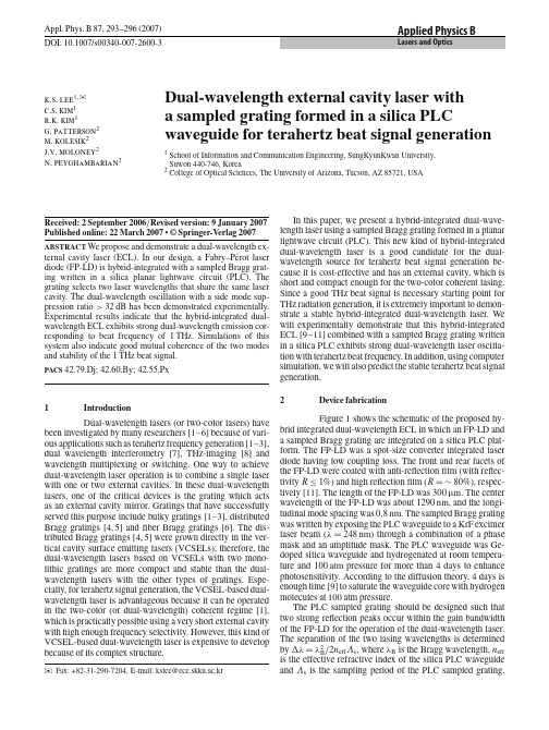
DOI:10.1007/s00340-007-2600-3Appl.Phys.B 87,293–296(2007)Lasers and OpticsApplied Physics Bk.s.lee 1,u c.s.kim 1r.k.kim 1g.patterson 2m.kolesik 2j.v.moloney 2n.peyghambarian 2Dual-wavelength external cavity laser with a sampled grating formed in a silica PLCwaveguide for terahertz beat signal generation1School of Information and Communication Engineering,SungKyunKwan University,Suwon 440-746,Korea2College of Optical Sciences,The University of Arizona,Tucson,AZ 85721,USAReceived:2September 2006/Revised version:9January 2007Published online:22March 2007•©Springer-Verlag 2007ABSTRACT We propose and demonstrate a dual-wavelength ex-ternal cavity laser (ECL).In our design,a Fabry–P´e rot laser diode (FP-LD)is hybrid-integrated with a sampled Bragg grat-ing written in a silica planar lightwave circuit (PLC).The grating selects two laser wavelengths that share the same laser cavity.The dual-wavelength oscillation with a side mode sup-pression ratio >32dB has been demonstrated experimentally.Experimental results indicate that the hybrid-integrated dual-wavelength ECL exhibits strong dual-wavelength emission cor-responding to beat frequency of 1THz.Simulations of this system also indicate good mutual coherence of the two modes and stability of the 1THz beat signal.PACS 42.79.Dj;42.60.By;42.55.Px1IntroductionDual-wavelength lasers (or two-color lasers)havebeen investigated by many researchers [1–6]because of vari-ous applications such as terahertz frequency generation [1–3],dual wavelength interferometry [7],THz-imaging [8]and wavelength multiplexing or switching.One way to achieve dual-wavelength laser operation is to combine a single laser with one or two external cavities.In these dual-wavelength lasers,one of the critical devices is the grating which acts as an external cavity mirror.Gratings that have successfully served this purpose include bulky gratings [1–3],distributed Bragg gratings [4,5]and fiber Bragg gratings [6].The dis-tributed Bragg gratings [4,5]were grown directly in the ver-tical cavity surface emitting lasers (VCSELs);therefore,the dual-wavelength lasers based on VCSELs with two mono-lithic gratings are more compact and stable than the dual-wavelength lasers with the other types of gratings.Espe-cially,for terahertz signal generation,the VCSEL-based dual-wavelength laser is advantageous because it can be operated in the two-color (or dual-wavelength)coherent regime [1],which is practically possible using a very short external cavity with high enough frequency selectivity.However,this kind of VCSEL-based dual-wavelength laser is expensive to develop because of its complex structure.u Fax:+82-31-290-7204,E-mail:kslee@ece.skku.ac.krIn this paper,we present a hybrid-integrated dual-wave-length laser using a sampled Bragg grating formed in a planar lightwave circuit (PLC).This new kind of hybrid-integrated dual-wavelength laser is a good candidate for the dual-wavelength source for terahertz beat signal generation be-cause it is cost-effective and has an external cavity,which is short and compact enough for the two-color coherent lasing.Since a good THz beat signal is necessary starting point for THz radiation generation,it is extremely important to demon-strate a stable hybrid-integrated dual-wavelength laser.We will experimentally demonstrate that this hybrid-integrated ECL [9–11]combined with a sampled Bragg grating written in a silica PLC exhibits strong dual-wavelength laser oscilla-tion with terahertz beat frequency.In addition,using computer simulation,we will also predict the stable terahertz beat signal generation.2Device fabricationFigure 1shows the schematic of the proposed hy-brid integrated dual-wavelength ECL in which an FP-LD and a sampled Bragg grating are integrated on a silica PLC plat-form.The FP-LD was a spot-size converter integrated laser diode having low coupling loss.The front and rear facets of the FP-LD were coated with anti-reflection film (with reflec-tivity R ≤1%)and high reflection film (R =∼80%),respec-tively [11].The length of the FP-LD was 300µm .The center wavelength of the FP-LD was about 1290nm ,and the longi-tudinal mode spacing was 0.8nm .The sampled Bragg grating was written by exposing the PLC waveguide to a KrF excimer laser beam (λ=248nm )through a combination of a phase mask and an amplitude mask.The PLC waveguide was Ge-doped silica waveguide and hydrogenated at room tempera-ture and 100atm pressure for more than 4days to enhance photosensitivity.According to the diffusion theory,4days is enough time [9]to saturate the waveguide core with hydrogen molecules at 100atm pressure.The PLC sampled grating should be designed such that two strong reflection peaks occur within the gain bandwidth of the FP-LD for the operation of the dual-wavelength laser.The separation of the two lasing wavelengths is determined by ∆λ=λ2B /2n eff Λs ,where λB is the Bragg wavelength,n eff is the effective refractive index of the silica PLC waveguide and Λs is the sampling period of the PLC sampled grating.294Applied Physics B –Lasers andOpticsFIGURE 1Configuration of a dual-wavelength external cavity laser with a sampled Bragg grating formed in a silica PLC waveguideThus,for n eff =1.45,the required sampling period Λs for gen-eration of 1THz beating signal is ∼103µm .The length of the sampled grating was adjusted to ∼10mm by using a shut-ter placed between the KrF excimer laser and the phase mask.One can also vary the strength of the grating by controlling the exposure time of the excimer laser beam because the strength is proportional to the UV exposure time.A number of PLC gratings with a pitch,Λ,of 450.91nm and different sampling periods Λs were written with the laser beam of fluence of 680mJ /cm 2at the repetition rate of 5Hz .In an ideal case,when the gain experienced by the two frequencies fed back in the laser by the sampled grating is ap-proximately equal,and the two modes are perfectly mutually coherent,the output intensity I (t )is modulated as [1]I (t )=I 1+I 2+2I 1I 2cos (2πf b t ),(1)where I 1and I 2are the laser mode intensities for the two dif-ferent wavelengths,and f b is the beat frequency of the two wavelengths.In reality,the lasing modes are only partially mutually coherent,and the amplitude of the modulation term in (1)decreases accordingly.Thus,a good dual-wavelength design must exhibit high mutual coherence between the lasing modes in order to achieve strong THz radiation generation.3Experimental resultsThe PLC gratings were grown after 900s-irradia-tion.Figure 2shows the transmission spectra of thePLCFIGURE 2Transmission spectra of the PLC sampled gratings used in the dual-wavelength external cavity laser with two different sam-pling periods,(a )Λs =∼100µm and (b )Λs =∼150µmsampled gratings used in the dual-wavelength external cavity lasers for two different sampling periods Λs =∼100µm and Λs =∼150µm .The two reflection peaks in Fig.2indicate that the PLC gratings act as an external cavity mirror feed-ing back two laser wavelengths.The two peak wavelengths of the PLC gratings with Λs =∼100µm are approximately at 1312.02nm and 1318.86nm ,as shown in Fig.2a.Those of the PLC gratings with Λs =∼150µm are 1313.08nm and 1317.02nm as shown in Fig.2b.The bandwidths of the reflec-tion peaks of the PLC gratings are measured to be ∼0.1nm ,which is limited to the resolution of the optical spectrum analyzer.The reflectivity of the reflection peaks ranges be-tween 80%and 94%.The wavelength spacing between the two peaks for Λs =∼100µm is ∼5.84nm ,while the spacing for Λs =∼150µm is ∼3.94nm .We demonstrated two different dual-wavelength ECLs using the PLC sampled gratings.The optical spectra of the dual-wavelength external cavity lasers with the PLC sam-pled gratings corresponding to the Fig.2a and b are shown in Fig.3a and b,respectively.Note that the FP-LD,which runs multi-mode without the external cavity feedback,becomes stabilized at two laser modes with sidemode suppression ratio (SMSR)>32dB after the hybrid integration on the silica PLC platform.The oscillation spectra of the PLC-based dual-wavelength ECL were measured at 25◦and at an injection current of 60mA .Figure 3a shows that the dual-wavelength ECL (with the grating with Λs =∼100µm )emits laser out-puts with equal intensity (i.e.,I 1=I 2)at 1313.04nm and 1318.74nm .Figure 3b shows that the dual-wavelength ECL with Λs =∼150µm oscillates with unequal intensity (i.e.,I 1=I 2)at 1313.08nm and 1317.14nm .This indicates that the laser output of the first ECL (Λs =∼100µm )results in a beat signal with f b ∼1THz and that of the second ECL (Λs =∼150µm )yields to the beat signal with f b ∼0.7THz .However,the dual-wavelength laser with equal intensity is ideal because it gives the modulation depth of unity (see (1)).Therefore,the first dual-wavelength ECL shown in Fig.3a is better than the second dual-wavelength ECL for the terahertz beat signal generation.The oscillation wavelengths of the dual-wavelength ECL were extremely stable and consistent with the Bragg wave-lengths of the PLC gratings.This is because the thermal sta-LEE et al.Dual-wavelength external cavity laser for terahertz beat signal generation295FIGURE3Optical spectra of the dual-wavelength external cavity laser with different grating sampling periods for two different bias conditions,(a)Λs=∼100µm and(b)Λs=∼150µmbility of the silica-based PLC gratings is excellent and the PLC gratings act as the external mirror of the PLC-based dual-wavelength ECLs.Also,the silica PLC waveguide was formed to be operating under the single-mode condition above 1300nm.Therefore,the two modes should be oscillating in the same fundamental spatial mode such that the mode overlapping is excellent.In this section,we experimentally demonstrated that our external cavity lasers,consisting of a FP-LD hybrid-integrated with a sampled Bragg grating writ-ten in a PLC,exhibit strong dual-wavelength emission whose corresponding beat frequency is about1THz.The beat fre-quency can be directly measured by an intensity autocorre-lator[2].But in this work we do not attempt to measure it directly;instead,we use computer simulation to demonstrate the terahertz beat signal generation from the hybrid-integrated dual-wavelength ECLs in the next section.4Simulated results and discussionSeveral two-color lasing regimes exists,among which the coherent two-color lasing regime is the most promising one for THz radiation generation[1].In order to operate the laser systems in this regime,it requires very short feedback loops and very narrow spectralfilters,preferentially integrated on a chip[1]as shown in Fig.1.To complement our experimental results,we use realistic computer simulations to assess the coherence properties and stability of our two-color source.We utilize the same simulation technology as in[1], with the core of the model based on a broad-band laser model capable of resolving semiconductor laser dynamics on very fast time scales while properly capturing all properties of the active structure[12].Our model consists essentially of two parts.Thefirst is the waveguide with the sampled grating,and the second is a Fabry–P´e rot semiconductor laser.Since we do not have access to details of the laser active structure,we re-sort to using an active structure model that should have similar properties,though the gain-maximum wavelength is slightly different from the lasing wavelength of the experimental laser. However,from the point of view of THz generation,details of the active structure are less important.In fact,the behav-ior observed here can be reproduced on a qualitative level with any similar active structure.On the other hand,the laser cav-ity and feedback properties are crucial[1].These parameters are,therefore,taken directly from the experiment.These pa-rameters are taken directly from the ly,we reproduce the mode spacing of the laser and both facet reflec-tivities.Also,we use experimental parameters for the sampled grating.We choose coupling coefficient that reproduces the experimental reflectivity spectrum by shifting the central fre-quency to match the gain peak of the modellaser.FIGURE4Simulation results of the dual-wavelength ECL with a sampled grating withΛs=∼100µm.(a)Optical spectrum and(b)laser output power exhibiting deep modulation(f b=∼1THz)296Applied Physics B–Lasers and OpticsFigure4a shows the simulated spectrum in the two-color operation regime.The two peaks correspond to two frequen-cies enforced by the sampled-grating feedback.The almost equal height of the two peaks means roughly equal output powers of the two lasing modes.Simulation shows that their relative intensitiesfluctuate only slightly on a nano-second time scale.To check the long-term stability,we have simu-lated the system over hundreds of microseconds.Indeed,the simulation showed that the two-color regime is stable and ex-hibits only smallfluctuations.The mutual coherence of the two lasing modes can be seen as a beat signal in the output intensity shown in Fig.4b.The depth of the modulation is almost100%indicating both equal-ized power and high mutual coherence of the lasing modes. Long-time simulation showed that the mutual coherence is stable and exhibits only smallfluctuations.Among the various two-color lasing regimes classified by Matus et al.in[1],our regime can be characterized as a coherent two-color regime, with a small multi-mode contribution.Thus,our simulations strongly indicate that the proposed design is highly suitable for THz beat signal generation.5ConclusionWe demonstrated experimentally and theoretically a hybrid-integrated dual-wavelength laser consisting of an FP-LD which is hybrid-integrated with a sampled Bragg grat-ing written in a silica PLC for terahertz beat signal gen-eration.The PLC sampled grating in this new design acts as an external mirror that forces the two laser wavelengths to share the same composite cavity,unlike the conventional dual-wavelength laser which often used two ing the PLC sampled gratings written with sampling periods of 100µm and150µm,we demonstrated two ECLs exhibit-ing simultaneous dual-wavelength emission corresponding to the beat signals of f b≈1THz and≈0.7THz,respectively. The dual-wavelength oscillation with a side-mode suppres-sion ratio>32dB has been demonstrated.Our simulation results also indicate that the two-color operation is stable and produces mutually highly coherent modes suitable for THz beat signal generation.Thus,our dual-wavelength ECL de-sign combines favorable manufacturing aspects with the de-sired high quality dual-wavelength operation.ACKNOWLEDGEMENTS This work was supported by the Ko-rea Science and Engineering Foundation(KOSEF)grant funded by the Korea government(MOST)(No.R01-2005-000-10252-0)and by AFOSR MRI grant F49620-02-1-0380.JVM acknowledges support from the Alexander von Humboldt Foundation.REFERENCES1M.Matus,M.Kolesik,J.Moloney,M.Hofmann,S.Koch,J.Opt.Soc.Am.B21,1758(2004)2C.Wang,C.Pan,Opt.Lett.20,1292(1995)3M.Tani,P.Gu,M.Hyodo,K.Sakai,T.Hidaka,Opt.Quantum Electron.30,503(2000)4P.Pellandini,R.Stanley,R.Houdre,U.Oesterle,M.Ilegems,C.Weis-buch,Appl.Phys.Lett.71,864(1997)5M.Brunner,K.Gulden,R.Hovel,M.Moser,J.Carlin,R.Stanley, M.Ilegens,IEEE Photon.Technol.Lett.12,1316(2000)6W.Wang,M.Cada,J.Seregelyi,S.Paquet,S.Mihailov,P.Lu,IEEE Photon.Technol.Lett.17,2436(2005)7C.Tilford,Appl.Opt.16,1857(1977)8B.Hu,M.Nuss,Opt.Lett.20,1716(1995)9J.H.Lim,G.Lim,K.S.Lee,J.H.Song,Y.K.Oh,S.T.Jung,T.Kim,Fiber Integ.Opt.24,73(2005)10J.H.Lim,J.H.Song,R.K.Kim,K.S.Lee,J.R.Kim,IEEE Photon.Tech-nol.Lett.17,2430(2005)11R.K.Kim,J.H.Lim,J.H.Song,K.S.Lee,IEEE Photon.Technol.Lett.18,580(2006)12M.Kolesik,J.V.Moloney,IEEE J.Quantum Electron.QE-37,936 (2001)。
Finisar Endurance 耐力光纤产品说明书

Fiber Optics for Military ApplicationsSolutions GuideFinisar designs and manufactures high-performance and reliable fiber optics products for military applications. With more than 25 years experience in the optical communications industry, Finisar is recognized as the world’s largest supplier and volume leader of optical components and sub-systems. The products featured in this solutions guide provide an overview of some optics tech-nology best suited for advanced military applications.Fiber Optics for Military ApplicationsEndurance ® Rugged, Compact 10 Gb/s TransceiverFinisar’s Endurance transceiver provides bi-directional optical data links at data rates from 125 Mb/s up to 10 Gb/s for harsh environments. It is interoperable with standard SFP/SFP+ pluggable modules and contains 2-wire serial communication interface for digital control and diagnostics.Endurance operates at a wide temperature range from -40C to 85C and available with anoptional conformal coating resistant to corrosive environments. It mounts directly to the Printed Circuit Board to handle excessive shock and vibration. Finisar’s 850nm oxide Vertical Cavity Surface Emitting Laser (VCSEL) is best-in-class for reliability and has excellent performance over temperature. Endurance has been qualified to additional military specifications for long-term aging, salt spray and vibration.At half the length of Small-Form Factor (SFF) modules, Endurance saves space on PrintedCircuit Boards and allows multiple modules to be mounted side-by-side for high-density edge port counts.3 GHz XFP-RF Wavelength-Tunable TransmittersFinisar’s XFP-RF transmitter is a small form factor hot-pluggable optical module that can be fully loaded with analog carriers from 50 MHz to 3000 MHz on a single wavelength for RF-over-Fiber applications. The transmitter wavelength can be tuned to any of the 43 different Dense Wavelength Division Multiplexing (DWDM) wavelengths across the entire C-band in less than 500 ms. With 43 transmitters, this allows up to 43 optical signals, each with a full RF load up to 3GHz, to be multiplexed onto a single optical fiber to provide high bandwidth capacity.Advanced RF Optical Detectors and ReceiversFinisar’s single and balanced photodetectors, which leverage advanced waveguide integrated photodiodes, offer a highly-linear frequency response from DC to over 100 GHz and high RF output power levels for Analog RF-over-Fiber applications. The detectors operate at variouswavelengths including 1310 nm and 1550 nm. Finisar also offers receivers mating these advancedphotodetectors with high-performance transimpedance amplifiers.SFFEnduranceOptical Sensors and Discrete ComponentsFinisar offers a broad array of optical sources that can be used for developing sensors for reflectiveand scattering applications such as gesture recognition, motion sensors, velocity measurement, 3D scanning, and turbidity measurements. Finisar’s laser components can also be utilized for atomic clocks, communication links in hazardous environments with transmitting power over fiber to operate the remote site and free-space, line-of-site communication data links.Finisar’s VCSELs products include single mode and multi-mode devices, spanning wavelength rangesfrom 780 to 1000nm and powers from sub-mW to >1W and can operate reliably across the entire industrial temperature range in hermetic and non-hermetic environments. Finisar also has custom optical sensor design and packaging capabilities that can deliver a product as simple as a TO-46 can with a VCSEL die or as complex as a touch-less velocity sensor with integrated electronics delivering an analog signal output.High-Efficiency Diffractive GratingsLightSmyth™ Technologies, a Finisar Company, provides high efficiency diffraction gratings for optical telecommunications, defense and biological markets. LightSmyth offers more than 100 grating products based on its record-breaking transmission grating platform. This includes gratings forpulse compression and high-power beam combining utilized in high-power industrial lasers andhigh energy laser (HEL) weapons.Optical IsolatorsFinisar’s optical isolators have low insertion loss and high isolation to prevent optical feedback into lasers and maintain optimal and consistent link performance. A proprietary bonding process, combined withyears of volume manufacturing experience, results in high reliability. The types of isolators include free-space isolators, isolators with fiber pigtails, and receptacle isolators.Optical PassivesFinisar has a wide-array of high-performance optical passive products including wavelength multiplexers and optical interleavers.Finisar’s Dense Wavelength Division Multiplexers (DWDM) enables up to 48 wavelengths to be combinedonto a single fiber for high-capacity transport. They utilize Thin Film Filter technology which offers flexibility from single to high port count and high integration from single MUX or DeMux to OADM (Optical Add-Drop Multiplexer) feature in one module. This product requires no electrical power, and offers a combination of low loss and high channel isolation along with long term reliability.Fiber Optics for Industrial ApplicationsThe Industrial Internet, also known as Industry 4.0, is bringing greater speed and efficiency to industries such as fac-tory automation, rail transportation, power generation, oil and gas development, and health care delivery. An enormous amount of data is collected, transported, and analyzed - all which requires a vast number of high-bandwidth inter-connections between a myriad of nodes such as machines, sensors, facilities, computers, data centers, and people. Industrial Ethernet is becoming the communication standard to network all of these devices.Fiber optic communication solutions provide high data rates, long distances, galvanic isolation, low flammable media, and good electromagnetic compatibility (EMC). As the world’s largest fiber optic components and subsystem manufacturer, Finisar is best positioned to provide the Fast Ethernet and Gigabit Ethernet solutions to interconnect the Industrial Internet.Fiber Optics for Industrial ApplicationsToday, industrial communications are dominated by copperconnections along with fiber optic links utilizing Light Emitting Diodes (LEDs) at low bit rates and short distances. With the rise of the Industrial Internet, communication links will need to support higher datarates such as Fast Ethernet (125 Mb/s) and Gigabit Ethernet (1 Gb/s). Distances for these links may span meters to hundreds of meters (Short-Reach) and even kilometers (Long-Reach). LED fiber optic technology cannot support the higher data rates at these link distances. Laser sources such as Vertical-Cavity Surface-Emitting Lasers (VCSELs) andDistributed Feedback (DFBs) satisfy these new requirements while being cost competitive with LED solutions.Since interconnections in industrial applications will be more critical, the availability of fiber optic links will be very important. Finisar has shipped 175 million fiber optic transceivers with VCSELs with a failure rate of less than 10 parts per million. Finisar transceivers have patented digital diagnostic functions that provide early warning if a fiber optic link will godown. This enables maintenance to be dispatched before a data link fails.Comparison of Fiber Optic CharacteristicsEvolution of Industrial Fiber OpticsEndurance® Rugged, Compact Laser TransceiversFinisar’s Endurance® transceiver provides two-way optical data links at data rates for Fast Ethernet, Gigabit Ethernet and 10 Gigabit Ethernet. It interoperates with standard SFP/SFP+ pluggable modules and contains 2-wire serial communication interface for digital control and diagnostics.The Endurance transceiver operates at a wide temperature range, from -40°C to 85°C, and comes with an optional conformal coating (resistant to corrosive environments). It mounts directly to the Printed Circuit Board to handle excessive shock and vibration. Endurance is qualified to military specifications for long-term aging, salt spray, and vibration.At half the length of Small-Form Factor (SFF) modules, the Endurance transceiver saves space on Printed Circuit Boards and allows multiple modules to be mounted side-by-side for high-density edge port counts.SFP/SFP+ Pluggable TransceiversFinisar’s Small-Form Factor Pluggable (SFP) transceivers provide tremendous flexibility forindustrial applications. Common equipment can be designed with generic SFP ports and later the optimal transceiver can be installed for the application. This reduces R&D investments and streamlines operations.Finisar has the broadest SFP/SFP+ portfolio in the industry to accommodate data rates from Fast Ethernet to 10 Gigabit Ethernet, and distances from meters to kilometers. There is also an SFP option for RJ45 copper links.SFPwire® Active Optical CableFinisar’s SFPwire® AOC is a rugged fiber optic cable with SFP+ transceivers directly attached eliminating optical interfaces and providing an even lower cost solution for data links. The transceiver ends plug into standard SFP ports on industrial Ethernet equipment.The SFPwire AOC also operates at data rates from Fast Ethernet to 10 Gigabit Ethernet. Various standard cable lengths are available from 1 meter to 20 meters.Finisar’s proprietary digital diagnostics can provide early warnings to issues in the data links.Example of Finisar Products in Industrial EthernetEndurance® Rugged, Compact Laser TransceiversIndustrial Ethernet Switch modules that mount on DIN railings on the factory floor, have embedded Endurance laser transceivers to provide the optical interface. The transceiver’srugged form-factor is qualified for shock, vibration, and hazardous environments. These switch modules are small and power efficient due to the Endurance transceiver. With the multi data rate capabilities, Switch modules operate at Fast Ethernet and can transition up to Gigabit Ethernet as more bandwidth is required. This equipment fully interoperates with SFP/SFP+ transceivers on the other end of the link.Link Details:Fiber Type: Glass, Single-mode Data Rate: Fast Ethernet (125 Mb/s), Gigabit Ethernet (1 Gb/s), or 10 GbE (10 Gb/s) Laser type: 1310nm Distributed Feedback (DFB)Distance: 10 kilometers (at Gigabit Ethernet and 10 Gigabit Ethernet)SFP/SFP+ Pluggable TransceiversThe Industrial Ethernet backbone platform is designed with open SFP/SFP+ ports. Depending on the fiber distances and/or data rate required for each link, the factory can choose the optimal SFP/SFP+ transceivers. For some very short links, the factory utilizes a copper SFP with a standard RJ45 interface.With the patented digital diagnostic capabilities on the transceivers, the Ethernet Switch can monitor the link characteristics, such as receive optical input power, and provide early warningalarms to maintenance if it starts to deteriorate.Endurance Laser TransceiverSFP/SFP+ Laser TransceiverSFP Copper TransceiverFinisar CPRI (Common Public Radio Interface) Reference GuideIntroductionThe Common Public Radio Interface (CPRI) initiative was formed in June of 2003 and defined a new standardized interface for the interconnect point between the radio equipment (RE) and radio equipment controller (REC) within the base station. Finisar has several modules in the SFP form factor that are ideal for CPRI and other wireless base station applications ranging from short reach to 80km or greater in link length and from 614.4 Mbit/s to 9830.4 Mbit/s or greater in transmission rate.System ArchitectureTo provide mobile network operators better deployment flexibility, the specification breaks down the traditional radio base station into two separate building blocks: the radio equipment control (REC) and the radio equipment (RE). This allows the RE to be located close to the antenna and the REC at a location that can be easily accessed. The concept is illustrated in Figure 1. Additionally, the CPRI system architecture features the flexibility to have multiple remote head ends feed into one controller.Figure 1. Illustration of the basic building blocks in a radio base station using CPRI.Radio Standards SupportedThe CPRI standard supports transmission of data between the REC and RE in both directions for a radio base station consisting of one REC and one or more RE compliant to the following radio standards:•3rd Generation Partnership Project (3GPP) Universal Terrestrial Radio Access (UTRA) Frequency divisionduplex (FDD). Release 9 March 2010;•3GPP E-UTRA Release 9 March 2010;•Universal Mobile telecommunication system (UMTS) and Evolved UMTS (E-UMTS);•3GPP GSM/EDGE RAN Release 9 December 2009;•WiMAX Forum Mobile System Profile v1.5 (2009-08).The interface supports a mix of different radio standards on a link and the support of future standards is not precluded.Physical Layer Specification (Layer 1)Time division multiplexing (TDM) is used to multiplex the information from different antenna carriers onto the data stream. The CPRI standard defines seven different options for line bit-rate on either electrical or optical links:614.4, 1228.8, 2457.6, 3072.0, 4915.2, 6144.0, & 9830.4 Mbit/s. The interface supports a continuous range of distances between a master and slave port as illustrated in the Finisar CPRI Compatibility Product Guide (see reverse). There is the option to use either multi-mode or single-mode fiber for the uplink or downlink, using the same optical connectors and building practices as for SFP transceivers.No protocol is specified in the interface standard and vendors are free to use any technique that is proven to reach the specified clock stability, and bit error ratio (BER) of 10-12 required to avoid the need for forward error correction (FEC). The data format uses standard 8/10B line coding according to the IEEE Standard. The CPRI document recommends the re-use of optical transceivers from the following high-speed serial link standards:•Gbit Ethernet: Standard IEEE 802.3-2002 clause 38 (1000BASE-SX/LX);•10 Gbit Ethernet: Standard IEEE 802.3-2005clause 53 (10GBASE-LX4);•Fiber Channel (FC-PI-4) –INCITS Rev 8;•InfiniBand Volume 2 Rel 1.1 (November 2002); and•10 Gbit Ethernet: Standard IEEE 802.3-2008clause 52 (10GBASE-S/L/E)Interconnecting With Optical LinksREC to RE links typically reside outside of temperature-controlled environments and therefore require equipment capable of withstanding extreme temperatures. Finisar has a broad portfolio of products that are extended and industrial temperature capable. Although the CPRI standard allows either electrical or optical links between the REC and RE, optical links are the most proficient method of connecting REC and RE at distances greater than several meters. Readily available in the Finisar portfolio are CPRI-compatible products that fulfill links anywhere from <10m all the way up to 80km or greater.Finisar Product CompatibilityIn addition to SFP form factor modules, Finisar now offers products in the SFP+ form factor which are backward compatible with SFP and allow for applications up to 16x the base CPRI rate and higher.Please refer to the Finisar CPRI Compatibility Product Guide (see reverse) and the Finisar website for productrecommendations and to find more detailed product information.Pluggable Optics for the Data CenterThe data center ecosystem is going through unprecedented growth and innovation as new players,new business models and new technologies converge. One of the key trends is the growing importance and evolving landscape of fiber optic technologies enabling new architectures and enhanced levels of performance in the data center.Fiber optics is no longer an optional technology, or only reserved for the toughest interconnect problems. Bandwidth, port density and low-power demands now require fiber optics. And fiber optics is now a pervasive, high-volume, low-cost set of technologies that make it an easy choice for switch interconnect and server I/O.Finisar is investing heavily in the data center. Our 10G, 40G and 100G fiber optic products are enablingthe highest bandwidth, highest density, lowest power and lowest total cost interconnect solutions on the market today. And we are already working on 400G and beyond. We are ready to partner with you to push optical interconnect technologies even further to enable unprecedented scale, bandwidth, flexibility and efficiency to the modern, highly-interconnected data center.The Modern Highly-Interconnected Data CenterSERVERS10G SFP+25G SFP2810G SFPwire AOCTOR/LEAFSWITCHES40G QSFP+4x10G QSFP+100G QSFP284x25G QSFP2810G SFP+25G SFP2810G SFPwire AOCROUTERS100G CFP4100G CFP2100G CFP 100G CFP2-ACOCORE/SPINE SWITCHES40G QSFP+100G QSFP2840G/100G Quadwire AOC100G CXP 100G C.wire AOC 120G/300G BOAFinisar Products for the Data CenterAustraliaSingaporeMal aysi a IsraelCaliforniaIndia TexasSwedenGermany PennsylvaniaCanadaBrazilJapan South Korea Italy UKChinaAbout FinisarFinisar is a global technology leader in optical communications components and subsystems. These products enable high-speed voice, video and data communications for networking, storage, wireless, and cable TV applications. For more than 25 years, Finisar has provided critical breakthroughs in optics technologies and has supplied system manufacturers with the production volumes needed to meet the expanding demand for network bandwidth. Finisar’s industry-leading products include optical transceivers, optical engines, active optical cables, optical components, optical instrumentation, ROADM & wavelength management, optical amplifiers, and RF-over-Fiber.。
Vertical cavity surface emitting laser and method

专利名称:Vertical cavity surface emitting laser andmethod for fabricating the same发明人:Kyu-Sub Kwak申请号:US10447017申请日:20030528公开号:US20040120376A1公开日:20040624专利内容由知识产权出版社提供专利附图:摘要:A vertical cavity surface emitting laser (VCSEL) is provided with an aperture for guiding a flow of electric currents. The aperture is defined by an oxide so that the aperture is formed to be substantially circular in shape. A method for fabricating thelaser is also disclosed. The structure of the (VCSEL) makes it possible to control the oxidation rates of an oxidable layer in which an aperture is formed for guiding the flow of electric currents of a VCSEL, by forming a mesa trench of the VCSEL in a segmented structure which has a predetermined number of segments. Accordingly, it is possible to form an aperture approximately in a circular shape, so that the light emitting angle and shape of the VCSEL are easily controlled.申请人:KWAK KYU-SUB更多信息请下载全文后查看。
1550 nm高对比度光栅的VCSEL(中英双语)

1550 nm high contrast grating VCSELChristopher Chase, Yi Rao, Werner Hofmann, and Connie J.Chang-Hasnain* Department of Eletrical Engineering and Computer Sciences, University of California, Berkeley,CA 94720, USAAbstract: We demonstrate an electrically pumped high contrast grating(HCG) VCSEL operating at 1550 nm incorporating a porton implant-defined aperture. Output powers of >1 mW are obtained at room temperature under continuous wave operation. Devices operate continuous wave at temperatures exceeding 60℃. The novel device design, which is grown in a single epitaxy step, may enable lower cost long wavelength VCSELs.References and Links1. C. J. Chang-Hasnain, “Tunable VCSEL,” IEEE J. Sel. Top. Quantum Electron. 6(6), 978–987(2000).2.M. Lackner, M. Schwarzott, F. Winter, B. Kögel, S. Jatta, H. Halbritter, and P. Meissner, “COand CO2 spectroscopy using a 60 nm broadband tunable MEMS-VCSEL at 1.55 μm,” Opt.Lett. 31(21), 3170–3172(2006).3.M. Ortsiefer, R. Shau, G. Böhm, F. Köhler, and M. C. Amann, “Low-threshold index-guided1.5 μm longwavelength vertical-cavity surface-emitting laser with high efficiency,” Appl.Phys. Lett. 76(16), 2179 (2000).4.W. Yuen, G. S. Li, R. F. Nabiev, J. Boucart, P. Kner, R. J. Stone, D. Zhang, M. Beaudoin, T.Zheng, C. He, K.Yu, M. Jansen, D. P. Worland, and C. J. Chang-Hasnain, “High-performance1.6 μm single-epitaxy top-emitting VCSEL,” Electron. Lett. 36(13), 1121–1123 (2000).5.S. Nakagawa, E. Hall, G. Almuneau, J. K. Kim, D. A. Buell, H. Kroemer, and L. A. Coldren,“88 °C, continuouswave operation of apertured, intracavity contacted, 1.55 μm vertical-cavity surface-emitting lasers,” Appl. Phys. Lett. 78(10), 1337 (2001).6.N.Nishiyama, C. Caneau, B. Hall, G. Guryanov, M. Hu, X. Liu, M. Li, R. Bhat, and C. Zah,“Long-Wavelength Vertical-Cavity Surface-Emitting Lasers on InP With Lattice Matched AlGaInAs-InP DBR Grown by MOCVD,” IEEE J. Sel. Top. Quantum Elec tron. 11(5), 990–998 (2005).7. A.Syrbu, A. Mereuta, A. Mircea, A. Caliman, V. Iakovlev, C. Berseth, G. Suruceanu, A.Rudra, E. Deichsel, and E. Kapon, “1550 nm-band VCSEL 0.76 mW singlemode output power in 20–80°C temperature range,” Electron. Lett. 40(5), 306 (2004).8. C.Mateus, M. Huang, L. Chen, C. Chang-Hasnain, and Y. Suzuki, “Broad-Band Mirror(1.12-1.62 μm) Using a Subwavelength Grating,” IEEE Photon. Technol. Lett. 16(7),1676–1678 (2004).9.M.C.Huang,Y.Zhou, and C. J. Chang-Hasnain, “A surface-emitting laser incorporating ahigh-index-contrast subwavelength grating,” Nat. Photonics 1(2), 119–122 (2007).10.Y. Zhou, M. C. Y. Huang, C. Chase, V. Karagodsky, M. Moewe, B. Pesala, F. G. Sedgwick,and C. J. Chang-Hasnain, “High-Index-Contrast Grating (HCG) and Its Applications in Optoelectronic Devices,” IEEE J. Sel.Top. Quantum Electron. 15(5), 1485–1499 (2009). 11. A.Haglund, J. Gustavsson, J. Bengtsson, P. Jedrasik, and A. Larsson, “Design and Evaluationof Fundamental-Mode and Polarization-Stabilized VCSELs With a Subwavelength Surface Grating,” IEEE J. Quantum Electron.42(3), 231–240 (2006).12.M.Ortsiefer, M. Gorblich, Y. Xu, E. Ronneberg, J. Rosskopf, R. Shau, and M. Amann,“Polarization Control in Buried Tunnel Junction VCSELs Using a Birefringent Semiconductor/Di electric Subwavelength Grating,” IEEE Photon. Technol. Lett. 22(1), 15–17 (2010).13.M.C. Y. Huang, Y. Zhou, and C. J. Chang-Hasnain, “A nanoelectromechanical tunable laser,”Nat. Photonics 2(3), 180–184 (2008).14. C. Chase, Y. Zhou, and C. J. Chang-Hasnain, “Si ze effect of high contrast gratings inVCSELs,” Opt. Express 17(26), 24002–24007 (2009).15.V. Karagodsky, B. Pesala, C. Chase, W. Hofmann, F. Koyama, and C. J. Chang-Hasnain,“Monolithically integrated multi-wavelength VCSEL arrays using high-contrast gratings,”Opt. Express 18(2), 694–699 (2010).16.W.Hofmann, C. Chase, M. Müller, Y. Rao, C. Grasse, G. Böhm, M. Amann, and C. J.Chang-Hasnain, “Long-Wavelength High-Contrast Grating Vertical-Cavity Surface-Emitting Laser,” IEEE Photon. J. 2(3), 415–422 (2010).17.P. Gilet, N. Olivier, P. Grosse, K. Gilbert, A. Chelnokov, I. Chung, and J. Mørk,“High-index-contrast subwavelength grating VCSEL,” in Vertical-Cavity Surface-EmittingLasers XIV, J. K. Guenter and K. D. Choquette, eds. (SPIE, 2010), V ol. 7615, p. 76150J.1. IntroductionLong wavelength VCSELs are promising as a low cost laser source for metro area access networks [1], high speed optical interconnects, and diode laser spectroscopy [2]. They have traditionally been more challenging to realize when compared to GaAs-based short wavelength VCSELs because of several additional technical challenges posed by the InP material system, the most difficult of which are the top mirror and current aperture.The InP system is challenging to form a current aperture in because there is no easily oxidizable material in the system, unlike GaAs in which an aluminum oxide current aperture can be easily formed. Traditionally this problem has been overcome by forming a buried tunnel junction in the VCSEL structure [3]. Other approaches to solving this problem have been shown using an oxide aperture formed after pseudomorphic growth of GaAs-based materials above the active region [4], or by etching away layers in the middle of the VCSEL structure [5]. These aperture approaches are technically challenging and add expense to mass manufacturing long wavelength VCSELs.In addition to the challenge of the current aperture, the p-side mirror on the VCSEL also poses problems. The index contrast available in the InGaAIAs/InGaAsP/InP material system is substantially smaller than other VCSEL material systems. This small index contrast means greater than 40 pairs of epitaxial DBR are required on both bottom and top of the VCSEL structure, an extremely challenging technological proposition from the standpoint of epitaxial growth.This necessitates an alternative approach to the p-side mirror of the VCSEL structure. Typically a short current spreading p-region followed by a tunnel junction with n- region and intra-cavity contacts is employed [3]. The top mirror is then formed by either evaporating a dielectric mirror [6], wafer fusing an epitaxially-grown DBR grown on another material system [7], using an Sb-based DBR [5], or a metamorphically grown GaAs/AIGaAs top DBR [4]. These options are technologically challenging from a growth and fabrication standpoint and relatively costly compared to using a monolithic structure already including a p-GaAs/A1GaAs DBR as is used in a short wavelength VCSEL.Our group has reported that a high contrast grating [8], a grating subwavelength in period made of high index bars completely surrounded by a low index media such as oxide or air, cantotally replace the top DBR in a VCSEL [9]. An HCG provides intrinsic polarization control to VCSELs [10], a highly sought feature. Previously subwavelength gratings have been shown to provide polarization differentiation in VCSELs [11, 12], but because they were not completely surrounded by a low index material, they do not provide enough reflectivity for a VCSEL to lase, so a mirror in addition to the subwavelength grating was still required. When integrated on a wavelength-tunable VCSEL, a much faster tuning speed can be achieved due to the small mass of the HCG compared to a conventional DBR [13, 14]. In addition, HCGs can be leveraged to make controllably-defined arrays of VCSELs operating at different wavelengths for use in applications such as wavelength division multiplexing [IS].Electrically-pumped HCG VCSELs have been demonstrated at wavelengths of 850 nm, 980 nm and recently 1.32 um [9,10,16,17]. Many potential applications for VCSE current aperture Ls in next generation access networks and passive optical networks (PONS) require the VCSELs to operate at 1.55 um, and the InP material system is the widespread choice for a 1.55um active region. Here we report for the first time a 1.55 um HCG VCSEL on an InP platform operating continuous wave at room temperature. Due to a great reduction in epitaxial layer thickness above the active region, we can use proton implantation to form a current aperture. This novel design, hence, enables only one epitaxy step and simple fabrication, a feature that is very promising to manufacture high yield, low cost, long wavelength VCSELs.2. VCSEL design and fabricationA cross section of the device is shown schematically in Fig. 1. It consists of, starting from the substrate side, 45 pairs of n-DBR, an InP heat sink layer, an active region with 6 GaAlInAs quantum wells, and a thin layer of p-GaAlInAs, followed by a tunnel junction. Above the tunnel junction there are 2 pairs of n-DBR, followed by a -1.8 um air gap and a 195 nm thick InP high contrast grating. The grating is 12 X 12 μm2wide in all cases described here. Electrical confinement is provided in the structure by a proton implantation at a depth near the tunnel junction. The size of the proton implant aperture is varied from 8 to 25 um. Contacts are deposited on the backside of the wafer and topside on a contact layer above the HCG layer and surrounding the etched HCG.Fig 1. Schematic of a 1550 nm VCSEL with a suspended TE-HCG in place of a typical top DBR. Current confinement isprovided through the use of a proton-implant-defined aperture.The HCG in this structure is~195 nm thick and has a period of~1070 nm and semiconductor width of ~370 nm. The grating is designed to highly reflect light with electric field polarized parallel to the direction of the grating bars (TE), but not to the orthogonal polarization (TM). The grating is optimized so that it has a wide tolerance to the air gap dimension for ease of fabrication. Figure 2(a) shows the simulated reflectivity of HCG as a function of wavelength and light polarization (TE light (blue) has its electric field polarized along the bar direction while TM (red) is polarized perpendicular to the grating bar direction). The simulation is performed using rigorous coupled wave analysis (RCWA) [18]. Over 99% of TE-polarized light is reflected, while only~50% of TM-polarized light is. Figure 2(b) shows the reflectivity of the TE light as a function of wavelength over a smaller reflectivity interval. The TE HCG is over 99% reflective over a 150 nm range. In this simulation, parameters are fixed at: a grating thickness of 195 nm, a period of 1075 nm, and a grating duty cycle of 35% (~370 nm InP/~700 nm air). The HCG material is InP with a refractive index of 3.17 in all cases.Fig.2. a) Reflectivity of the HCG as a function of wavelength and polarization. The grating is highly reflective for TE light (blue, light with electric field polarized along the direction of the grating), and much less so for TM light (red, light polarized perpendicular to the direction of the grating). b) Zoomed in reflectivity of the TE polarization. The grating is over 99%reflective over a bandwidth of 150 nm.Device fabrication was carried out as follows. A current aperture was formed by protecting the aperture area by a thick photoresist, followed by a H + ion implantation with a dosage between 1014cm-2to 1015cm-2 and energy between 250keV to 400keV. A top annular n-contact subsequently was fabricated by lithography, metal evaporation and lift-off. A mesa was etched around the contact ring to the depth of the n-DBRs to electrically isolate the devices from each other.The HCG was defined by electron beam lithography and transferred by several steps of wet etching. In principle, the pattern could also be defined using a standard DUV lithography stepper. The HCG is then released by a selective etch of a sacrificial region below the HCC followed by critical point drying to prevent the structure from being damaged during the drying process. A scanning electron microscope (SEM) image of a completed HCG VCSEL is shown in Fig. 3(a). A zoomed in SEM image of the HCG is shown in Fig. 3(b).Fig. 3. SEM images of a (a) a completed 1550 nm HCG VCSEL (b) Zoomed in image of the high contrast grating, which is just195 nm thick.3.Characteristics3.1 Light-current-voltage characteristicsA series of VCSELs were fabricated with an identical HCG size of 12 X 12 um2and various implant aperture sizes, ranging from 5 to 20 um. The fabricated devices show excellent electrical and optical characteristics. Figure 4(a) shows the light-current (solid) and voltage-current (dashed) characteristics of a VCSEL with a 13 um proton implant aperture at various heat sink temperatures. The VCSELs have a threshold current of~3 mA at room temperature (AT) and lase continuous wave (CW) at temperatures exceeding 60 ℃. The RT peak output power is ~1.1 mW with slope efficiencies >0.25 mW/mA. Other devices with slightly higher thresholds showed up to 1.4 mW peak output powers at room temperature. The devices show a differential resistance of 60-100 Ω depending on aperture size.Fig.4. a) Light-current (solid lines) and voltage-current (dashed lines) characteristics of a HCG VCSEL with a 13 μm proton implant aperture at various heat sink temperatures. Devices show over 1.1 mW output power at room temperature and operate continuous wave to >60° C.b) Spectrum of the same device under various heat sink temperatures. A wavelength shift of0.12nm/K is extractedFigure 4 (b) shows its optical spectrum at a constant bias current of 8 mA at various heat sink temperatures. A wavelength shift of 0.12 nm/K is observed. A thermal resistance of 1.55 K/mW is also obtained, indicating good heat transfer away from the active region. At all biases the VCSELs emit in a single transverse mode with a side mode suppression ratio > 45dB. Single mode emission was seen in VCSELs with proton implant aperture size up to 20um. It should be noted though that the HCG is only 12 X 12 μm2, so the finite HCG size is also providing some transverse mode discrimination.3.2 Optical mode characteristicsFavorable optical mode characteristics for optical communications applications are also obtained due to the use of the HCG and a proton implant aperture. An important characteristic for VCSELs for mid-and long-reach optical communications links is polarization stability, as any polarization instability can have deleterious effects on an optical link. HCG VCSELs are polarization stable due to the high differentiation between the reflectivity in the orthogonal electric field polarizations as is shown in Fig. 2(a). Figure 5(a) shows the polarization-resolved light-current characteristics of a device with a 15 um proton implant aperture and 12 X12um2 HCG. The orthogonal polarization is suppressed by >20 dB (limited by the polarizer in the experimental setup).Since proton implant defined apertures provide little optical index guiding, it is possible to achieve larger size apertures while maintaining a single transverse mode emission profile .This makes the devices ideal for high coupling efficiency to a single mode fiber. The near-field intensity profile of a device with a 15 um proton implant aperture and 12 X12um2 HCG is shown in Fig. 5(b). This device emits in a single fundamental transverse mode with a full width half maximum (FWHM) of ~6.5 um. Generally, the devices have FWHMs of 40-50% of their lithographically defined aperture size. VCSFLs with >20 um proton-implant-defined apertures show no significant higher order transverse mode, since the finite area of HCG reflectivity (12 X12um2)contributes to the suppression of the higher order transverse modes in the largest aperture devices.Fig.5. a) Polarization-resolved light-current characteristics of a 1550 nm HCG VCSEL. A polarization suppression ratio of >20 dB is achieved, with the measurement limited by the polarizer. b) Near field intensity profile of the device at 2.5 X I th. A FWHM of ~6.5μm is obtained with a VCSEL with a proton implant aperture size of 15 μm.4.ConclusionWe present a 1550 nm VCSEL utilizing an HCG as a top mirror and proton implantation to form an electrical aperture. These devices can be simply fabricated using a monolithic epitaxial growth without the need for additional regrowth or dielectric mirror deposition.These devices have >1 mW output power at room temperature and operate continuous wave to greater than 60℃. Single mode operation is achieved with large apertures and no degenerate polarization modes. This simple VCSEL structure is promising for manufacturable, low-cost, long wavelength VCSEL for optical communications applications.AcknowledgementsThe authors would like to acknowledge support from the National Science Foundation through CIAN NSP ERC under grant #EEC-0812072 and a National Science Foundation Graduate Research Fellowship. We also thank the Berkeley Microfabrication Laboratory for their fabrication support.(译文)1550 nm高对比度光栅的VCSEL克里斯托弗大通,易扰,沃纳霍夫曼,康妮J.Chang - Hasnain *电子工程与计算机科学系,加州大学伯克利分校,加州94720,美国摘要:我们展示了一个工作在1550nm波长集成了波顿植入定义光圈的电动泵高对比度光栅(HCG)的VCSEL。
清华考博辅导:清华大学电子科学与技术考博难度解析及经验分享 (2)

清华考博辅导:清华大学电子科学与技术考博难度解析及经验分享根据教育部学位与研究生教育发展中心最新公布的第四轮学科评估结果可知,全国共有74所开设电子科学与技术类专业的大学参与了排名,其中排名第一的是电子科技大学,排名第二的是西安电子科技大学,排名第三的是北京大学。
作为清华大学实施国家“211工程”和“985工程”的重点学科,电子工程系的电子科学与技术一级学科在历次全国学科评估中均名列第四。
下面是启道考博整理的关于清华大学电子科学与技术考博相关内容。
一、专业介绍清华大学电子科学与技术是属于清华大学电子工程系,电子科学与技术是信息科学技术的前沿学科,它以现代物理学与数学为基础,研究电子、光子的运动及在不同介质中的相互作用规律,研究采用计算机与信息处理技术,发明和发展各种信息电子材料和元器件、信息光电子材料和器件、集成电路和集成电子系统。
我系电子科学与技术专业的研究方向为物理电子学与光电子学。
物理电子学与光电子学主要内容为: 集成光电子学;纳米光子学;光纤通信系统与光网络智能化技术;光电子器件与应用技术;新型显示和新型电光薄膜材料与器件; 信息纳米材料与器件;大功率高速电子器件;微细技术和信息光电子材料评价与检测技术; 光电信息传感技术等。
本专业设有集成光电子学国家重点实验室 (清华大学实验区), 超净工艺线和电子系统集成与专用集成电路技术研究中心。
清华大学电子工程系电子科学与技术专业在博士招生方面,划分为十个研究方向:080900 电子科学与技术博士研究方向:01 物理电子与光电子学02 电路与系统03 电磁场与微波理论及技术04 感知智能与纳米传感器05 新能源及生物医疗光电子技术06 电磁场与微波理论及技术、新型电磁材料07 生物光子学08 多模态数据处理系统与脑神经系统信息挖掘09 脑机接口系统集成技术及其生物医疗应用10 界面电磁学的理论与应用此专业实行申请考核制。
二、考试内容清华大学管理电子科学与技术专业博士研究生招生为资格审查加综合考核形式,由笔试+专业面试+英语口语构成。
光与物质相互作用英文
光与物质相互作用英文Light-Matter Interaction.Light and matter interact in a variety of ways,including absorption, emission, scattering, and reflection. These interactions are essential for many natural phenomena, such as photosynthesis, vision, and the colors of objects. They are also used in a wide range of technologies, such as lasers, solar cells, and optical fibers.Absorption.When light is absorbed by matter, the energy of thelight is transferred to the matter. This can cause the matter to become excited, which can lead to a change in its chemical or physical properties. For example, absorption of light can cause a molecule to dissociate, or it can causean electron to be promoted to a higher energy level.Emission.When matter emits light, the energy of the light comes from the matter itself. This can happen when an excited atom or molecule returns to its ground state, or it can happen when an electron recombines with a hole. Emission of light is the basis for many light sources, such as lasers and LEDs.Scattering.When light is scattered by matter, the direction of the light is changed. This can happen when light interacts with particles that are smaller than the wavelength of light, or it can happen when light interacts with rough surfaces. Scattering of light is responsible for the blue color of the sky and the white color of clouds.Reflection.When light is reflected by matter, the direction of the light is changed, but the wavelength of the light remains the same. This can happen when light interacts with asmooth surface, such as a mirror, or it can happen when light interacts with a transparent material, such as glass. Reflection of light is used in a variety of applications, such as mirrors, lenses, and optical fibers.The interaction of light with matter is a complex and fascinating topic. It is essential for understanding a wide range of natural phenomena and technologies.Here are some additional details about each of the four types of light-matter interactions:Absorption.When light is absorbed by matter, the energy of the light is transferred to the matter. This can cause the matter to become excited, which can lead to a change in its chemical or physical properties. For example, absorption of light can cause a molecule to dissociate, or it can cause an electron to be promoted to a higher energy level.The amount of light that is absorbed by matter dependson the wavelength of the light and the properties of the matter. Some materials, such as metals, are very good at absorbing light, while other materials, such as glass, are very poor at absorbing light.Emission.When matter emits light, the energy of the light comes from the matter itself. This can happen when an excited atom or molecule returns to its ground state, or it can happen when an electron recombines with a hole.The wavelength of the light that is emitted by matter depends on the energy difference between the two states involved in the transition. For example, when an electron recombines with a hole in a semiconductor, the energy difference between the two states is typically in the visible range, so the emitted light is visible light.Scattering.When light is scattered by matter, the direction of thelight is changed. This can happen when light interacts with particles that are smaller than the wavelength of light, or it can happen when light interacts with rough surfaces.The amount of light that is scattered by matter depends on the size and shape of the scattering particles and the wavelength of the light. For example, small particles scatter light more effectively than large particles, and short-wavelength light is scattered more effectively than long-wavelength light.Reflection.When light is reflected by matter, the direction of the light is changed, but the wavelength of the light remains the same. This can happen when light interacts with a smooth surface, such as a mirror, or it can happen when light interacts with a transparent material, such as glass.The amount of light that is reflected by matter depends on the refractive index of the material. The refractive index is a measure of how much light is bent when it passesfrom one material to another. Materials with a high refractive index, such as glass, reflect more light than materials with a low refractive index, such as air.。
Transceiver laser
• Surface emitting device (high yield –can be optically tested before dicing) • narrow spectral width (can be SLM) • Very low threshold current (<1mA to 7mA) • High speed (depending on design) – can be used at data rates from 155 Mbps to >10 Gbps • Output current (bias plus modulation) must remain above the laser threshold current to avoid turn-on delay and optimize speed • Some device exhibit a behavior called “off-state bounce” which can result in slower fall times • VCSELs (Vertical Cavity Surface-Emitting Lasers) include geometries, circular output beams, high fiber optic coupling efficiencies, extremely low power consumption, and high modulation rates.
Welcome!
1. Abstract
• Fabry-Perot Laser (FP)
• Distributed Feedback Laser (DFB) • Light Emitting Diode (LED) • Vertical Cavity Surface-Emitting Laser (VCSEL) • Photo Diode (PD) • Pin-Transimpedance (PIN-TIA) • Transceiver
(整理)光学英语词汇.
A01光学材料:A01-001 光学材料 Optical MaterialsA01-002 光学玻璃 Optical GlassA01-003 激光玻璃 Laser GlassA01-004 声光玻璃 Acousto-Optic Glass ,acoustic有关声音的, 声学的, 音响学的A01-005 红外线玻璃 Infrared GlassA01-006 红外线材料 Infrared MaterialsA01-007 紫外线材料 Ultraviolet MaterialsA01-008 石英镜片 Fused Silica GlassA01-009 光学陶瓷 CeramicsA01-010 矽半导体材料Silicon Semiconductor MaterialsA01-011 化合物半导体材料Compound Semiconductor MaterialsA01-012 光纤材料 Fiber Optic MaterialsA01-013 光纤预型体 Fiber Optic PreformsA01-014 PLZT晶圆,钛酸锆酸铅晶圆 PLZT WafersA01-015 环氧树脂 EpoxiesA01-016 声光光学晶体 Acousto-Optic CrystalsA01-017 双折射/偏光晶体 Birefringent and Polarizing CrystalsA01-018 电光光学晶体 Electro-Optic CrystalsA01-019 红外线晶体 Infrared CrystalsA01-020 激光晶体 (YAG) YAG Laser CrystalsA01-021 激光晶体(亚历山大) Alexandrite Laser CrystalsA01-022 激光晶体(GGG) GGG Laser CrystalsA01-023 激光晶体(GSGG,GSAG) GSGG GSAG Laser CrystalsA01-024 激光晶体(YLF) YLF Laser CrystalsA01-025 激光晶体(其他) Other Laser CrystalsA01-026 非线性光学晶体 Nonlinear CrystalsA01-027 有机光学材料 Organic Optical MaterialsA01-028 萤光放射晶体 Fluorescent Emission CrystalsA01-029 结晶育成材料 Crystals Growing MaterialsA01-030 镀膜材料 Coating MaterialsA01-031 光罩材料 Photomask MaterialsA01-032 真空蒸镀化学药品 Vaccum Evaporation ChemicalsA01-033 感光剂 SensitizersA01-034 影像用材料 Materials for ImagingA01-035 热色材料 Thermochromic MaterialsA01-036 光色材料 Photochromic MaterialsA01-037 稀土族材料 Rare Earth MaterialsA01-038 光碟基板,基板材料 Optical Disk Substrate MaterialsA01-039 光碟记录材料 Optical Disk Data Storage MaterialsA02 加工用其他材料 MATERIALS FOR PROCESSINGA02-001 光学用胶合剂/接著剂 Optical Cements and AdhesivesA02-002 光学用气体 Gases for Optical ApplicationA02-003 激光用气体 Gases for LasersA02-004 光学研磨材料(研磨布纸) Optical-Coated AbrasiveA02-005 光学研磨材料(砥粒) Optical-Powder or Grin AbrasiveA02-006 光学研磨材料(砥石) Optical-Wheel AbrasiveA02-007 研磨化合物 Polishing CompoundsA02-008 研磨衬垫及布 Polishing Pads and ClothA02-009 全像底片及感光板 Holographic Films and PlatesA02-010 红外线底片及感光板 Infrared Films and PlatesA02-011 相片用化学药品 Photographic ChemicalsA02-012 折射率液 Refractive Index LiquidsA02-013 显微镜浸液 Microscope Immerison LiquidsA02-014 显微镜埋置用材料 Microscope Imbedding MediaA02-015 激光用染料 Laser DyesA02-016 冷媒 CoolantsA02-017 拭镜纸 Lens TissueA03 显示器用材料 MATERIALS FOR DISPLAYA03-001 液晶 Liquid CrystalsA03-002 导电膜玻璃基板 ITO Glass SubstrateA03-003 彩色滤光片 Color FilterA03-004 偏光板/相位差板 Polarizer/ Phase Shift LayerA03-005 显示面板用驱动IC Driver ICA03-006 背光源 BacklightA03-007 配向膜 Alignment FilmA03-008 间隔物SpacerB01 透镜 LENSESB01-001 单透镜 Simple (Single) LensesB01-002 球透镜 Ball LensesB01-003 歪像透镜 Anamorphic LensesB01-004 圆锥透镜 Conical LensesB01-005 柱状透镜,环形透镜 Cylindrical & Toroidal LensesB01-006 非球面透镜 Aspheric LensesB01-007 反射折射透镜 Catadioptric LensesB01-008 绕射极限透镜 Diffraction-Limited LensesB01-009 GRIN透镜 GRIN Lenses (Graduated Refractive Index Rod)B01-010 微小透镜阵列 Micro Lens ArraysB01-011 准直透镜 Collimator LensesB01-012 聚光透镜 Condenser LensesB01-013 多影像透镜 Multiple Image LensesB01-014 傅利叶透镜 Fourier Lenses B01-015 菲涅尔透镜 Fresnel Lenses B01-016 替续透镜 Relay LensesB01-017 大口径透镜(直径150mm以上) Large Aperture Lenses (150mm)B01-018 复合透镜 Complex LensesB01-019 红外线透镜 Infrared LensesB01-020 紫外线透镜 Ultraviolet LensesB01-021 激光透镜 Laser LensesB01-022 望远镜对物镜 Telescope Objectives LensesB01-023 显微镜对物镜 Microscope Objectives LensesB01-024 接目镜 Eyepieces LensesB01-025 向场透镜 Field LensesB01-026 望远镜头 Telephoto LensesB01-027 广角镜头 Wide Angle LensesB01-028 可变焦伸缩镜头 Variable Focal Length Zoom LensesB01-029 CCTV镜头 CCTV LensesB01-030 影印机镜头 Copy Machine LensesB01-031 传真机镜头 Facsimile LensesB01-032 条码扫描器镜头 Bar Code Scanner LensesB01-033 影像扫描器镜头 Image Scanner LensesB01-034 光碟机读取头透镜 Pick-up Head LensesB01-035 APS相机镜头 APS Camera LensesB01-036 数位相机镜头 Digital Still Camera LensesB01-037 液晶投影机镜头 Liquid Crystal Projector LensesB02 镜面 MIRRORB02-001 平面镜 Flat MirrorsB02-002 球面凹面镜,球面凸面镜 Spherical Concave and Convex Mirrors B02-003 抛物面镜,椭圆面镜 Off-Axis Paraboloids and Ellipsoids Mirrors B02-004 非球面镜 Aspheric MirrorsB02-005 多面镜 Polygonal MirrorsB02-006 热镜 Hot MirrorsB02-007 冷镜 Cold MirrorsB02-008 玻璃,玻璃/陶瓷面镜 Glass and Glass-Ceramic MirrorsB02-009 双色向面镜 Dichroic MirrorB02-010 金属面镜 Metal MirrorsB02-011 多层面镜 Multilayer MirrorsB02-012 半涂银面镜 Half-Silvered MirrorsB02-013 激光面镜 Laser MirrorsB02-014 天文用面镜 Astronomical MirrorsB02-099 其他面镜 Other MirrorsB03 棱镜 PRISMB03-001 Nicol棱镜 Nicol PrismsB03-002 Glan-Thomson棱镜 Glan-Thomson PrismsB03-003 Wollaston棱镜 Wollaston PrismsB03-004 Rochon棱镜 Rochon PrismsB03-005 直角棱镜 Right-Angle; Rectangular PrismsB03-006 五面棱镜 Pentagonal PrismsB03-007 脊角棱镜 Roof PrismsB03-008 双棱镜 BiprismsB03-009 直视棱镜 Direct Vision PrismsB03-010 微小棱镜 Micro PrismsB03-099 其他棱镜 Other PrismsB04 滤光镜 FILTERB04-001 尖锐滤光镜 Sharp Cut (off) FiltersB04-002 色温变换滤光镜,日光滤光镜 Colour Conversion/Daylight FiltersB04-003 干涉滤光镜 Interference FiltersB04-004 中性密度滤光镜 Neutral Density FiltersB04-005 空间/光学匹配滤光镜 Spatial/Optical Matched FiltersB04-006 双色向滤光镜 Dichroic FiltersB04-007 偏光滤光镜 Polarizing FiltersB04-008 排除频带滤光镜 Rejection Band FiltersB04-009 可调式滤光镜 Turnable FilterB04-010 超窄频滤光镜 Ultra Narrowband FiltersB04-011 色吸收滤光镜 Absorption FiltersB04-012 红外吸收/反射滤光镜 Infrared Absorbing/Reflecting FiltersB04-013 红外透过滤光镜Infrared Transmitting FiltersB04-014 紫外吸收滤光镜Ultraviolet Absorbing FiltersB04-015 紫外透过滤光镜 Ultraviolet Transmitting FiltersB04-016 针孔滤光镜 Pinhole FiltersB04-017 有色玻璃滤光镜 Colored-Glass FiltersB04-018 塑胶滤光镜 Plastic FiltersB04-019 照像用滤光镜 Photographic FiltersB04-020 全像滤光镜 Holographic FiltersB04-021 微小干涉滤光镜 Micro Interference FiltersB06 激光 LASERSB06-100 气体激光 GAS LASERSB06-101 氦氖激光 He-Ne LasersB06-102 金属蒸气激光 Metal Vapor LasersB06-103 氩离子激光 Argon LasersB06-104 氪离子激光 Krypton LasersB06-105 二氧化碳激光(气流型) CO2 (Gas Flow type) LasersB06-106 二氧化碳激光(脉冲,TEA型) CO2 (Pulsed,TEA) LasersB06-107 二氧化碳激光(密封型) CO2 (Sealed tube) LasersB06-108 二氧化碳激光(波导型) CO2 (Wave guide) LasersB06-109 一氧化碳激光 CO Lasers B06-110 氦镉激光 He-Cd LasersB06-111 氮分子激光 Nitrogen LasersB06-112 准分子激光 Excimer LasersB06-113 氙分子激光 Xenon LasersB06-200 固体激光 SOLID STATE LASERSB06-201 红宝石激光 Ruby LasersB06-202 玻璃激光 Glass LasersB06-203 Nd:YAG激光(脉冲式) Nd:YAG (Pulsed) LasersB06-204 Nd:YAG激光(连续式) Nd:YAG Laser (CW) LasersB06-205 Nd:YAG激光(半导体激光激发) Nd:YAG (LD Pumped) LasersB06-206 YLF激光 YLF LasersB06-207 亚历山大激光 Alexanderite LasersB06-208 铒固体激光 Erbium LasersB06-209 半导体激光激发式固态激光 Solid State(LD pumped)LaserB06-210 其他固态激光 OthersB06-300 染料激光 DYE LASERSB06-301 染料激光(闪光灯激发) Dye (Flash lamp Pumped) LasersB06-302 染料激光(激光激发) Dye (Laser Pumped) LasersB06-400 半导体激光 SEMICONDUCTOR LASERSB06-401 半导体激光(1.55μm带) Semiconductor (1.55μm) LasersB06-402 半导体激光(1.30μm带) Semiconductor (1.30μm) LasersB06-403 半导体激光(0.85μm带) Semiconductor (0.85μm) LasersB06-404 半导体激光(0.78μm带) Semiconductor (0.78μm) LasersB06-405 半导体激光(0.60μm带) Semiconductor (0.60μm) LasersB06-406 半导体激光(其他波长带) Other Semiconductor LasersB06-407 半导体激光模组(长波长) Semiconductor (Long Wavelength) Laser ModulesB06-408 半导体激光模组(短波长) Semiconductor (Short Wavelength) Laser ModulesB06-409 半导体激光模组(可见光) Semiconductor (Visible) Laser ModulesB06-501 铁离子中心激光 F-Center LasersB06-502 化学激光(HF-DF) Chemical (HF-DF) LasersB06-503 平板激光 Slab LasersB06-504 远红外线激光 Far-Infrared LasersB06-505 真空紫外线激光 Vacuum Ultraviolet LasersB06-506 多色激光 Multi Colour LasersB06-507 稳频激光 Frequency Stabilized LasersB06-508 自由电子激光 Free Electron LasersB07 激光用元件 LASER COMPONENTSB07-001 Q 开关 Laser Q-SwitchesB07-002 激光管 Laser Tubes and BoresB07-003 激光棒 Laser RodsB07-004 激光板 Laser SlabsB07-005 气体再生设备,气体填充设备 Gas Recyclers and Gas Handling EquipmentB07-006 激光控制设备 Laser Control EquipmentB07-007 激光用盒 Laser CellsB07-008 参数振汤器 Parametric OscillatorsB07-009 光脉冲产生设备 Optical Pulse GeneratorsB07-010 激光用共振腔 Resonators for LasersB07-011 磁铁 MagnetsB07-012 激光用冷却设备 Cooling Systems for LasersB07-013 激光护眼镜 Safty Equipment; Goggles Glasses and FilmsB07-014 激光光吸收体 Safty Equipment; Laser AbsorbersB07-015 激光用安全设备 Safty Equipment; Protective HousingsB08 发光二极体 LIGHT-EMITTING DIODES; LEDB08-001 通信用1.55μm发光二极体 1.55μm LEDs for CommunicationB08-002 通信用1.30μm发光二极体 1.30μm LEDs for CommunicationB08-003 通信用0.85μm发光二极体 0.85μm LEDs for CommunicationB08-004 通信用长波长发光二极体模组 Long Wavelength LED Modules for CommunicationB08-005 通信用短波长发光二极体模组 Short Wavelength LED Modules for CommunicationB08-006 可见光发光二极体(红色) Visible (Red) LEDsB08-007 可见光发光二极体(黄色) Visible (Yellow,Orange) LEDsB08-008 可见光发光二极体(绿色,多色) Visible (Green,Multi-Color) LEDsB08-009 可见光发光二极体(蓝色) Visible (Blue) LEDsB08-010 红外线二极体(非通信用) Infrared (not for Communication) LEDsB08-011 文数字表示用发光二极体 Alpha-Numeric LEDsB08-012 发光二极体晶圆(通信用) LED Wafers for CommunicationB08-013 发光二极体晶圆(非通信用) LED Wafers not for CommunicationB08-014 发光二极体晶片、晶粒(通信用) LED Chips for CommunicationB08-015 发光二极体晶片、晶粒(非通信用) LED Chips not for CommunicationB09 光源设备 LIGHT SOURCESB09-001 标准光源 Standard Light SourcesB09-002 安定化光源 Stabilized Light SourcesB09-003 弧光灯 Arc Light SourcesB09-004 氪灯 Krypton Light SourcesB09-005 卤素灯 Halogen Light SourcesB09-006 氙灯 Xenon /Xenon Flashlamps Light SourcesB09-007 紫外线光源 Ultraviolet Light SourcesB09-008 真空紫外线光源 VUV Light SourcesB09-009 红外线光源 Infrared Light SourcesB09-010 闪光光源 Stroboscopic Light SourcesB09-011 小型光源 Miniature Light SourcesB09-012 光纤光源 Fiber Optic IlluminatorsB10 显示器元件 DISPLAY PANELB10-001 发光二极体显示器 LED DisplaysB10-002 液晶显示器 Liquid Crystal Display (LCD)B10-003 电浆显示器 Plasma Display Panels(PDP)B10-004 电激发光显示器 Electroluminescence Display (ELD)B10-005 电铬显示器 Electrochromic Display (ECD)B10-006 真空萤光显示器 Vacuum Fluorescent Display (VFD)B10-007 平面阴极射线管 Flat CRTsB10-008 场发射显示器 Field Emitter Display(FED)B10-099 其他平面显示元件 Other Flat Panel DisplaysB11 检光元件及光纤混成元件 DETECTORS & FIBEROPTIC HYBRID DEVICESB11-001 通信用PIN光二极体 PIN Photodiodes for CommunicationB11-002 通信用崩溃光二极体 Avalanche Photodiodes for CommunicationB11-003 通信用(长波长)Ge和III-V族检光元件Long-wavelength Detectors for CommunicationB11-004 通信用PIN光二极体模组 PIN Photodiode Modules for CommunicationB11-005 通信用崩溃光二极体模组 Avalanche Photodiode Modules for CommunicationB11-006 通信用(长波长)Ge和III-V族检光模组 Long-wavelength Decector Modules for CommunicationB11-007 光二极体(近红外光) Near-infrafed PhotodiodesB11-008 光二极体(可见光) Visible PhotodiodesB11-009 光二极体(紫外光) Ultraviolet PhotodiodesB11-010 光电晶体 PhototransistorsB11-011 光电管 PhototubesB11-012 光电子增倍管(PMT) PhotomultipliersB11-013 光导电池 Photoconductive CellsB11-014 热电偶检测器 Thermocouple DetectorsB11-015 热堆检测器 Thermopile DetectorsB11-016 微道板 Microchannel PlatesB11-017 热电检测器 Pyroelectroic DetectorsB11-018 辐射热测定器 BolometersB11-019 其他红外线检测器 Infrared DetectorsB11-020 摄像管 Camera TubesB11-021 线型检光元件 One Dimension Detector ArraysB11-022 面型检光元件 Two Dimension Detector ArraysB11-023 光电耦合器 Photo CouplerB11-024 光断续器 Photo InterrupterB11-025 光反射器 Photo ReflectorB11-026 光闸流晶体管 PhotocyristorsB11-027 光感测元件 Photosensing UnitsB11-028 内藏电路之光感测器 Detectors with CircuitB11-029 民用用太阳电池 Solar Cells for Consumer UseB11-030 产业用太阳电池 Solar Cells for Power & Space UseB12 光纤及光缆 FIBER OPTIC FIBERS & CABLEB12-100 光纤 FIBER OPTIC FIBERSB12-101 石英系多模态步阶式折射率型光纤 Fiber Optic Fibers, Silica, Multimode, Step IndexB12-102 石英系多模态渐近式折射率型光纤(50/125) Fiber Optic Fibers, Silica, Multimode, Graded Index,50/125B12-103 石英系多模态渐近式折射率型光纤(62.5/125) Fiber Optic Fibers, Silica, Multimode,Graded Index ,62.5/125B12-104 石英系多模态渐近式折射率型光纤(100/140) Fiber Optic Fibers, Silica, Multimode,Graded Index ,100/140B12-105 石英系单模态标准型光纤 Fiber Optic Fibers, Silica, Single Mode,StandardB12-106 色散位移光纤 Fiber Optic Fibers, Dispersion – ShiftedB12-107 偏振恒持光纤 Fiber Optic Fibers, Polarization – MaintainingB12-108 其他单模态光纤 Other Single Mode Optic FibersB12-109 石英系塑胶包覆光纤 Fiber Optic Fibers, Plastic - Clad SilicaB12-110 塑胶光纤 Fiber Optic Fibers, PlasticB12-111 石英系影像光纤 Fiber Optic Bundles, Silica, ImagingB12-112 多成分影像光纤 Fiber Optic Bundles, Non-silica, ImagingB12-113 光导管 Fiber Optic LightguidesB12-199 其他集束光纤 Other Fiber Optic BundlesB12-200 光缆 FIBER OPTIC CABLEB12-201 单模态标准型松包悬空式光缆 Fiber Optic Cable, Single Mode, Standard, Loosely Buffered, AerialB12-202 单模态标准型松包管路式光缆 Fiber Optic Cable, Single Mode, Standard, Loosely Buffered, DuctB12-203 单模态标准型松包直埋式光缆 Fiber Optic Cable, Single Mode, Standard, Loosely Buffered, Direct BuriedB12-204 单模态标准型紧包单心式光缆 Fiber Optic Cable, Single Mode, Standard, Tightly Buffered, Single FiberB12-205 单模态标准型紧包多心式光缆 Fiber Optic Cable, Single Mode, Standard, Tightly Buffered, MultifiberB12-206 光纤带 RibbonB12-207 色散位移光缆 Fiber Optic Cable, Dispersion-ShiftedB12-208 偏振恒持光缆 Fiber Optic Cable, Polarization – MaintainingB12-209 其他单模态光缆 Other Single Mode Fiber Optic CableB12-210 多模态石英系(50/125)光缆 Fiber Optic Cable, Multimode, Silica, 50/125B12-211 多模态石英系(62.5/125)光缆 Fiber Optic Cable, Multimode, Silica, 62.5/125B12-212 多模态石英系(100/140)光缆 Fiber Optic Cable, Multimode, Silica, 100/140B12-213 塑胶光缆 Fiber Optic Cable, PlasticB12-214 石英系塑胶包覆光缆 Fiber Optic Cable, Plastic-Clad SilicaB12-215 其他多模态光缆 Other Multimode Fiber Optic CableB12-216 光纤保护用管 Protect Tubes for Fiber Optic FiberB13 光被动元件/光控制元件 OPTICAL PASSIVE DEVICES/CONTROL DEVICESB13-001 单模态ST光纤连接器 Fiber Optic Connectors, Single Mode, STB13-002 单模态Biconic光纤连接器 Fiber Optic Connectors, Single Mode, BiconicB13-003 单模态FC/PC光纤连接器 Fiber Optic Connectors, Single Mode, FC/PCB13-004 单模态APC光纤连接器 Fiber Optic Connectors, Single Mode, APCB13-005 单模态FDDI光纤连接器 Fiber Optic Connectors, Single Mode, FDDIB13-006 单模态SC光纤连接器 Fiber Optic Connectors, Single Mode, SCB13-007 单模态D4光纤连接器 Fiber Optic Connectors, Single Mode, D4B13-008 单模态光纤连接器插座(ST,FC/PC,SC,Biconic) Fiber Optic Connectors, Single Mode, Adapter(ST,FC/PC,SC,Biconic)B13-009 单模态多心光纤连接器(MT) Fiber Optic Connectors, Single Mode,Multi-Channel/MT B13-010 其他单模态光纤连接器 Other Single Mode Fiber Optic ConnectorsB13-011 多模态ST光纤连接器 Fiber Optic Connectors, Multimode, STB13-012 多模态FC/PC相容光纤连接器 Fiber Optic Connectors, Multimode, FC/PCB13-013 多模态SMA光纤连接器 Fiber Optic Connectors, Multimode, SMAB13-014 多模态FDDI光纤连接器 Fiber Optic Connectors, Multimode, FDDIB13-015 多模态SC光纤连接器 Fiber Optic Connectors, Multimode, SCB13-016 多模态D4光纤连接器 Fiber Optic Connectors, Multimode, D4B13-017 多模态光纤连接器插座(ST,SMA,FC/PC) Fiber Optic Connectors, Multimode,Adapter(ST,SMA,FC/PC)B13-018 多模态多心光纤连接器 Fiber Optic Connectors, Multimode, Multi-ChannelB13-019 其他多模态光纤连接器 Other Multimode Fiber Optic ConnectorsB13-020 套筒 SleevesB13-021 金属箍(套管) Metal FerrulesB13-022 塑胶箍(套管) Plastic FerrulesB13-023 陶瓷箍(套管) Ceramic FerrulesB13-024 插座 ReceptaclesB13-025 插头 PlugsB13-026 光连接器(含光纤线) Optical Connectors with FiberB13-027 光纤耦合器(两分支) Optical Couplers, Tap/SplitterB13-028 光纤耦合器(树状分支) Optical Couplers, TreeB13-029 星状光纤耦合器(穿透形) Transmission Type Star Optical CouplersB13-030 星状光纤耦合器(反射形) Reflection Type Star Optical CouplersB13-031 其他光纤耦合器 Other Optical CouplersB13-032 光分波合波器(两波长) Optical Couplers, WDM, Dual-WavelengthB13-033 光分波合波器(多波长) Optical Couplers, WDM, Over Two WavelengthB13-034 其他光分波合波器 Other Optical WDM CouplersB13-035 光衰减器(固定) Fixed Optical AttenuatorsB13-036 光衰减器(可变) Adjustable Optical AttenuatorsB13-037 光隔离器(通信用) Optical Isolators for CommunicationB13-038 光隔离器(非通信用) Optical Isolators for Non-CommunicationB13-039 光环流器 Optical CirculatorsB13-040 光开关(机械式) Mechanical Optical SwitchesB13-041 光开关(非机械式) Non-mechanical Optical SwitchesB13-042 光纤光栅 Fiber Bragg GratingB13-043 光移相器 Optical Phase ShiftersB13-044 光共振器 Optical ResonatorsB13-045 空间调变元件 Spatial Light ModulatorsB13-046 光影像转换元件(ITC) Incoherent to Coherent Devices(ITC)B13-047 光截波器,机械式光调变器 Optical Choppers, Mechanical ModulatorsB13-048 磁光调变器 Maganeto-Optic ModulatorsB13-049 声光调变器 Acousto-Optic ModulatorsB13-050 电光调变器 Electro-Optic ModulatorsB13-051 波导形调变器,行波形调变器 Optical Waveguide,Travelling-wave ModulatorsB13-052 类比/强度调变器 Analog/Intensity ModulatorsB13-053 数位调变器 Digital ModulatorsB13-054 其他调变器 Other ModulatorsB13-055 光弹性调变器 Photoelastic ModulatorsB13-056 机械式偏折/扫瞄器(Galvanometer方式) Mechanical Optical Deflectors/Scanners(Galvanometer Mirror)B13-057 声光偏折/扫瞄器 Acousto-Optic Optical Deflectors/ScannersB13-058 电光偏折/扫瞄器 Electro-Optic Optical Deflectors/ScannersB13-059 机械式扫瞄器(回转多面镜方式) Mechanical Optical Scanners(Polygonal Mirrors) B13-060 机械式扫瞄器(全像方式) Mechanical Optical Scanners(Holographic)B13-061 光纤跳接线 Fiber Optic Patchcord PigtailB13-062 光纤终端箱 Fiber Optic Distribution BoxB13-063 光纤接续盒 Fiber Optic ClosureB13-099 其他光被动元件/控制元件 Other Optical Passive Devices/Control DevicesB14 积体光元件 INTEGRATED OPTICAL DEVICESB14-001 光IC Optical ICB14-002 OEIC Optoelectronic ICB14-099 其他光电元件 Other DevicesC01 光通讯设备 OPTICAL COMMUNICATION EQUIPMENTC01-100 电信用光通讯设备 OPTICAL COMMUNICATION EQUIPEMNT(TELECOMMUNICATION)C01-101 同步光纤网路光波传输系统及多工机设备 Lightwave/Transimission System and Multiplexer Equipment (SONET-Based)C01-102 同步光纤网路光数位回路载波机设备 Optical/Digital Loop Carrier Equipment (SONET-Based)C01-103 同步光纤网路数位交换连接系统设备 Digital Cross Connect System Equipment (SONET-based)C01-104 同步数位阶层光波传输系统及多工机设备 Lightwave/Transmission System and Multiplexer Equipment (SDH-Based)C01-105 同步数位阶层光数位回路载波机设备 Optical/Digital Loop Carrier Equipment (SDH-Based)C01-106 同步数位阶层数位交换连接系统设备 Digital Cross Connect System Equipment (SDH-Based)C01-107 光纤网路单体 ONU(Optical Network Unit)C01-108 非同步光通讯设备 Asynchronous Optical Communication EquipmentC01-199 其他公众用光通讯设备 Other Optical Communication Equipment (Telecommunication) C01-200 数据通讯光纤网路设备 OPTICAL DATA COMMUNICATION NETWORK EQUIPMENT (PREMISES) C01-201 光纤分散式资料介面网路设备 FDDI Network EquipmentC01-202 非同步传输模式网路设备 ATM Network EquipmentC01-203 高速乙太网路设备 Fast Ethernet Network EquipmentC01-204 光纤通道 Fiber ChannelC01-299 其他用户光数据通讯设备 Other Optical Data Communication Network Equipment (Premises)C01-300 特殊用途光传输设备 OPTICAL TRANSMISSION EQUIPMENT(SPECIAL PURPOSE)C01-301 有线电视光传输设备 Optical Transmission Equipment, CATVC01-302 视讯/闭路监视光传输设备 Optical Transmission Equipment, Video/CCTVC01-303 量测/控制信号光传输设备 Optical Transmission Equipment, Measure/ControlC01-304 空间(无线)光传输设备 Optical Transmission Equipment, Spatial (Wireless)C01-305 光放大器 Optical AmplifierC01-399 其他特殊用途光传输设备 Other Optical Transmission Equipment (Special Purpose)C02 光测仪器设备 OPTICAL MEASURING EQUIPMENTC02-001 量测用标准光源 Standard/Stabilized Light SourcesC02-002 光功率计(热转换型) Thermal Conversion Type Optical Power MetersC02-003 光功率计(光电转换型) Photoelectric Conversion Type Optical Power MetersC02-004 光谱分析仪 Optical Spectrum AnalyzersC02-005 光波长计 Optical Wavelength MetersC02-006 光谱幅宽量测器 Spectral Width Measuring EquipmentC02-007 光时域反射计(OTDR) Optical Time-Domain Reflectometers(OTDR)C02-008 基频传输特性检测器 Baseband Frequency Characteristics Evaluation EquipmentC02-009 波长色散量测器 Wavelength Dispersion Measuring EquipmentC02-010 光纤测试设备 Optical Fiber Test EquipmentC02-011 激光光束波形量测器 Laser Beam Profile Measuring EquipmentC02-012 光纤尺寸量测器 Optical Fiber Sizes Measuring EquipmentC02-013 光纤模态参数测试器 Optical Fiber Mode Field Parameters Test EquipmentC02-014 光纤强度测试器 Optical Fiber Strength Test EquipmentC02-015 其他光纤相关量测设备 Other Optical Fiber Measurement EquipmentC02-016 光连接器尺寸量测器 Optical Connector Sizes Measuring EquipmentC02-017 光碟测定检查设备(装置用) Optical Disk Drive Inspection EquipmentC02-018 光碟测定检查设备(碟片用) Optical Disk Inspection EquipmentC02-019 光度计 PhotometersC02-020 复光束光度计,复光束量测器 Double Beam PhotometersC02-021 测微光度计 MicrophotometersC02-022 感光密度计 DensitometersC02-023 光泽度计 GrossmetersC02-024 照度计 Illuminance MetersC02-025 测距仪 RangefindersC02-026 曝光计 Exposure MetersC02-027 辉度计 Luminance MetersC02-028 比色计 Comparison ColorimetersC02-029 色彩计(分光型) Spectral ColorimetersC02-030 色彩计(光电型) Photoelectric ColorimetersC02-031 积分球 Integrating SpheresC02-032 折射计 RefractometersC02-033 椭圆计 EllipsometersC02-034 偏振光镜 PolariscopesC02-035 偏振计 PolarimetersC02-036 比较量测器 ComparatorsC02-037 焦距仪 FocometersC02-038 球径计 SpheremetersC02-039 OTF(光学转换函数)设备 Optical Transfer Function InstrumentationC02-040 MTF分析/量测装置Modulation Transfer Function(MTF) Analysis/Measurement EquipmentC02-041 投影检查器 Profile ProjectorsC02-042 自动准直仪 AutocollimatorsC02-043 光弹性机器 Photoelastic InstrumentsC02-099 其他光(学)量测器 Other Optical Measurement EquipmentC03 分光镜、干涉仪 SPECTROSCOPES, INTERFEROMETERSC03-001 分光计 SpectrometersC03-002 单色器 MonochromatorsC03-003 分光镜,干涉分光镜,摄谱仪Spectroscopes, Interference Spectroscopes,SpectrographsC03-004 分光光度计,分光测光器 SpectrophotometerC03-005 Michelson干涉仪 Michelson InterferometersC03-006 Tywman Green干涉仪 Tywman Green InterferometersC03-007 Mach-Zehnder干涉仪 Mach-Zehnder InterferometersC03-008 Fizeau干涉仪 Fizeau InterferometersC03-009 Fabry-Perot干涉仪 Fabry-Perot InterferometersC04 显微镜,望远镜,照像机 MICROSCOPES, TELESCOPES, CAMERASC04-001 放大镜 MagnifiersC04-002 单接物镜双眼显微镜 Binocular MicroscopesC04-003 双眼实体显微镜,立体显微镜 Stereo MicroscopesC04-004 金属显微镜 Metallurgical MicroscopesC04-005 偏光显微镜 Polarizing MicroscopesC04-006 相位差显微镜 Phase-Contrast MicroscpoesC04-007 干涉显微镜,微分干涉对比显微镜Interferences/Differential Interference Contrast MicroscopesC04-008 萤光显微镜 Fluorescence MicroscopesC04-009 激光显微镜 Laser MicroscopesC04-010 量测用显微镜,工具显微镜 Measurement MicroscopesC04-011 显微镜光度计 Microscope PhotometersC04-012 折射望远镜,Galilean望远镜 Galilean Refracting TelescopesC04-013 反射望远镜 Reflecting TelescopesC04-014 反射折射望远镜 Catadioptric TelescopesC04-015 35mm焦平面自动对焦相机 35mm AF Focal Plane CamerasC04-016 35mm焦平面手动对焦相机 35mm NON-AF Focal Plane CamerasC04-017 35mm镜头快门多焦点相机 35mm Multi Focal Points Lens Shutter CamerasC04-018 35mm镜头快门单焦点相机 35mm Single Focal Point Lens Shutter CamerasC04-019 中,大型照相机 Medium and Large Size CamerasC04-020 VTR摄影机 VTR CamerasC04-021 电视摄影机 TV CamerasC04-022 高画质电视摄影机 High Definition(HDTV) CamerasC04-023 CCTV摄影机 CCTV CamerasC04-024 全像照像机 Holographic CamerasC04-025 眼镜 EyeglassesC04-026 夜视设备 Night Vision EquipmentC04-027 照像机用之日期显示模组 Date moduleC04-028 照像机用之底片计数器 Film counterC04-029 APS相机 APS CamerasC05 光感测器 OPTICAL SENSORSC05-001 光电开关,光电感测器 Photo Switches, Photo SensorsC05-002 标记感测器 Mark Photo SensorsC05-003 色彩标记感测器 Color Mark Photo SensorsC05-004 色彩感测器 Color Photo SensorsC05-005 光学式编码器,角度感测器 Optical Encoders, Angle SensorsC05-006 光遥控器 Optical Remote Control EquipmentC05-007 影像感测器式量测设备 Image Sensor Type Measurement InstrumentsC05-008 显微镜式量测设备 Microscope Type Measurement InstrumentsC05-009 精密长度干涉仪 Precise Length InterferometersC05-010 光波测距装置 Electronic Distance MetersC05-011 三角测量法距离感测器 Triangulation Distance MetersC05-012 激光调变测距方式距离感测器 Laser Modulation Distance MetersC05-013 脉冲测距方式距离感测器 Pulse Distance MetersC05-014 激光外径测定器 Laser Outer Diameter Measuring SensorsC05-015 激光厚度计 Laser Thickness GaugesC05-016 激光拉伸计 Laser Extension MeterC05-017 红外线厚度计 Infrared Thickness GaugesC05-018 水平仪 LevelsC05-019 激光水平仪 Laser LevelsC05-020 经纬仪 Theodlites/TransitsC05-021 激光经纬仪 Laser Theodlites/TransitsC05-022 激光标线设备 Laser Marking-off EquipmentC05-023 位置光电感测器 Position Sensors, Pattern Edge SensorsC05-024 半导体位置感测器 Position Sensitive Devices(PSDs)C05-025 激光指示器 Laser PointersC05-026 激光都卜勒测速计 Laser Doppler VelocimetersC05-027 环形激光流速计,光纤陀螺仪 Ring Laser Velocimeters, Optical Fiber Laser Gyros C05-028 转速仪 Rotational Speed MetersC05-029 激光都卜勒转速仪 Laser Doppler Rotational Speed MetersC05-030 全像方式图样量测设备 Holographic Method Pattern Measurement EquipmentsC05-031 激光移位计 Laser Displacement MetersC05-032 激光指纹检测器 Laser Fingerprint DetectorsC05-033 光学水质污染检测设备Optical Water Pollution Measurement and Detection EquipmentC05-034 光学大气污染检测设备 Optical Air Pollution Measurement and Detection Equipment C05-035 红外线气体浓度感测器 Infrared Gas Density MetersC05-036 光电式烟检知器 Photo Smoke DetectorsC05-037 激光粉尘监视器,粒径量测器 Laser Dust MonitorsC05-038 距离测定用激光雷达 Rang-finding Lidar SystemsC05-039 环境监测用激光雷达 Environment Monitoring Lidar SystemsC05-040 激光表面检查设备 Laser Surface Inspection EquipmentC05-041 平面度测定系统 Flatness TestersC05-042 斑点图形量测设备 Speckle Method Pattern Measurement EquipmentC05-043 云纹图形量测设备 Moire Method Pattern Measurement EquipmentC05-044 影像分析仪 Image AnalyzersC05-045 激光缺陷检查设备 Laser Defect Inspection EquipmentC05-046 红外线辐射温度感测器 Infrared ThermometersC05-047 人体检知感测器,激光保全设备 Laser Security/Surveillance EquipmentsC05-048 光计数器 Photo CountersC05-049 激光公害检测设备 Laser Pollution Detective DevicesC05-050 激光热常数量测设备 Laser Thermal Constants Measurement EquipmentC05-051 全像非破坏检查设备 Holographic Nondestructive Testing EquipmentC06 光纤感测器 FIBER OPTIC SENSORSC06-001 光纤光电开关/感测器 Fiber Optic Photo Switches/ SensorsC06-002 光纤式标记感测器 Fiber Optic Mark Photo SensorsC06-003 光纤式色彩标记感测器 Fiber Optic Color Mark Photo SensorsC06-004 光纤温度感测器 Fiber Optic Temperature SensorsC06-005 光纤压力感测器 Fiber Optic Pressure SensorsC06-006 光纤声波感测器 Fiber Optic Acoustic SensorsC06-007 光纤变形感测器 Fiber Optic Strain SensorsC06-008 光纤振动感测器 Fiber Optic Vibration SensorsC06-009 光纤移位感测器 Fiber Optic Displacement SensorsC06-010 光纤陀螺仪感测器 Fiber Optic Gyro SensorsC06-011 光纤速度感测器 Fiber Optic Velocity SensorsC06-012 光纤磁通量感测器 Fiber Optic Magnetic Flux SensorsC06-013 光纤磁场感测器 Fiber Optic Magnetic Field SensorsC06-014 光纤电流感测器 Fiber Optic Current SensorsC06-015 光纤电场感测器 Fiber Optic Electric Field SensorsC06-016 光纤浓度、成份感测器 Fiber Optic Density,Constituent SensorsC06-017 光纤油膜感测器 Fiber Optic Oil Film SensorsC06-018 光纤液位感测器 Fiber Optic Liquid Surface Level SensorsC06-019 光纤光分布/放射线感测器 Fiber Optic Light Distribution/Radiation Sensors C06-020 光纤显微镜 Fiber Optic FiberscopesC06-021 光纤光栅应变感测器 Fiber Grating Strain SensorC07 光储存装置 OPTICAL STORAGE PRODUCTC07-100 消费性光碟机 CONSUMER OPTICAL DISC PLAYERSC07-101 激光唱盘 Compact Disc (CD) PlayersC07-102 激光音响组合 Products Incorporated CD(CD-Radio-Cassette Tape Recorders)C07-103 LD 影碟机 Laser Disc (LD) PlayersC07-104 影音光碟机 Video CD PlayersC07-105 DVD DVD 影碟机 Digital Versatile Disc (DVD) PlayersC07-106 迷你音碟机 Mini Disc (MD) PlayersC07-200 资讯用仅读型光碟机 READ-ONLY OPTICAL DISC DRI597VESC07-201 CD-ROMCD-ROM光碟机 CD-ROM DrivesC07-202 DVD-ROM DVD-ROM 光碟机 DVD-ROM DrivesC07-300 资讯用仅写一次型光碟机 RECORDABLE OPTICAL DISC DRIVESC07-301 CD-R CD-R 光碟机 CD-R DrivesC07-399 其他仅写一次型光碟机 Other Recordable Optical Disc DrivesC07-400 资讯用可覆写型光碟机 REWRITABLE OPTICAL DISC DRIVESC07-401 3.5" MO 光碟机 3.5" MO Disc DrivesC07-402 5.25" MO 光碟机 5.25" MO Disc DrivesC07-403 PD 光碟机 PD DrivesC07-404 CD-RW光碟机 CD-RW DrivesC07-499 其他可覆写型光碟机 Other Rewritable Optical Disc DrivesC07-500 光碟机零组件 DEVICES OF OPTICAL DISC DRIVESC07-501 光学头,光学读取头 Optical Heads , Pick-up HeadsC07-502 光学头伺服装置,伺服用IC模组 Optical Head Controllers, Control ICs/Modules C07-503 光学头驱动装置 Optical Head ServomotorsC07-504 光碟匣 Optical Disc Cartridges。
1550nm垂直腔面发射激光器设计
Key Words: VCSEL DBR photonic crystal wafer fusion
目录
目录
第一章 绪论.....................................................................................................................1 1.1 半导体激光器.....................................................................................................1 1.2 垂直腔表面发射激光器的历史现状﹑特点和结构.........................................2 1.2.1 垂直腔表面发射激光器的历史..............................................................2 1.2.2 垂直腔面发射激光器的特点和应用......................................................3 1.2.3 垂直腔表面发射激光器的结构..............................................................3 1.3 长波段 VCSEL 的研究状况 ..............................................................................5 1.4 光子晶体的历史和原理.....................................................................................6 1.5 本论文的研究工作及意义.................................................................................8
与激光有关的英文文献
与激光有关的英文文献Revised at 16:25 am on June 10, 2019L a s e r t e c h n o l o g y R. E. Slusher Bell Laboratories, Lucent Technologies, Murray Hill, New Jersey 07974 Laser technology during the 20th century is reviewed emphasizing the laser’s evolution from science to technology and subsequent contributions of laser technology to science. As the century draws to a close, lasers are making strong contributions to communications, materials processing, data storage, image recording, medicine, and defense. Examples from these areas demonstrate the stunning impact of laser light on our society. Laser advances are helping to generate new science as illustrated by several examples in physics and biology. Free-electron lasers used for materials processing and laser accelerators are described as developing laser technologies for the next century.S0034-68619902802-01. INTRODUCTIONLight has always played a central role in the study of physics, chemistry, and biology. Light is key to both the evolution of the universe and to the evolution of life on earth. This century a new form of light, laser light, has been discovered on our small planet and is already facilitating a global information transformation as well as providing important contributions to medicine, industrial material processing, data storage, printing, and defense. This review will trace the developments in science and technology that led to the invention of the laser and give a few examples of how lasers are contributing to both technological applications and progress in basic science. There are many other excellent sources that cover various aspects of the lasers and laser technology including articles from the 25th anniversary of the laser Ausubell and Langford, 1987 and textbooks ., Siegman, 1986; Agrawal and Dutta, 1993; and Ready, 1997.Light amplification by stimulated emission of radiation LASER is achieved by exciting the electronic, vibrational, rotational, or cooperative modes of a material into a nonequilibrium state so that photons propagating through the system are amplified coherently by stimulated emission. Excitation of this optical gain medium can be accomplished by using optical radiation, electrical current and discharges, or chemical reactions. The amplifying medium is placed in an optical resonator structure, for example between two high reflectivity mirrors in a Fabry-Perot interferometer configuration. When the gain in photon number for an optical mode of the cavity resonator exceeds the cavity loss, as well as loss from nonradiative and absorption processes, the coherent state amplitude of the mode increases to a levelwhere the mean photon number in the mode is larger than one. At pump levels above this threshold condition,the system is lasing and stimulated emission dominates spontaneous emission. A laser beam is typically coupled out of the resonator by a partially transmitting mirror. The wonderfully useful properties of laser radiation include spatial coherence, narrow spectral emission, high power, and well-defined spatial modes so that the beam can be focused to a diffraction-limited spot size in order to achieve very high intensity. The high efficiency of laser light generation is important in many applications that require low power input and a minimum of heat generation.When a coherent state laser beam is detected using photon-counting techniques, the photon count distribution in time is Poissonian. For example, an audio output from a high efficiency photomultiplier detecting a laser field sounds like rain in a steady downpour. This laser noise can be modified in special cases, ., by constant current pumping of a diode laser toobtain a squeezed number state where the detected photons sound more like a machine gun than rain. An optical amplifier is achieved if the gain medium is not in a resonant cavity. Optical amplifiers can achievevery high gain and low noise. In fact they presently have noise figures within a few dB of the 3 dB quantum noise limit for a phase-insensitive linear amplifier, ., they add little more than a factor of two to the noise power of an input signal. Optical parametric amplifiers OPAs, where signal gain is achieved by nonlinear coupling of a pump field with signal modes, can be configured to add less than 3 dB of noise to an input signal. In an OPA the noise added to the input signal can be dominated by pump noise and the noise contributed by a laser pump beam can be negligibly small compared to the large amplitude of the pump field.2. HISTORYEinstein 1917 provided the first essential idea for the laser, stimulated emission. Why wasn’t the laser invented earlier in the century Much of the early work on stimulated emission concentrates on systems near equilibrium, and the laser is a highly nonequilibrium system. In retrospect the laser could easily have been conceived and demonstrated using a gas discharge during the period of intense spectroscopic studies from 1925 to 1940. However, it took the microwave technology developed during World War II to create the atmosphere for thelaser concept. Charles Townes and his group at Columbia conceived the maser microwave amplification by stimulated emission of radiation idea, based on their background in microwave technology and their interest in high-resolution microwave spectroscopy. Similar maser ideas evolved in Moscow Basov and Prokhorov, 1954 and at the University of Maryland Weber, 1953. The first experimentally demonstrated maser at Columbia University Gordon et al., 1954, 1955 was based on an ammonia molecular beam. Bloembergen’s ideas for gain in three level systems resulted in the first practical maser amplifiers in the ruby system. These devices have noise figures very close to the quantum limit and were used by Penzias and Wilson in the discovery of the cosmic background radiation.Townes was confident that the maser concept could be extended to the optical region Townes, 1995. The laser idea was born Schawlow and Townes, 1958 when he discussed the idea with Arthur Schawlow, who understood that the resonator modes of a Fabry-Perot interferometer could reduce the number of modes interacting with the gain material in order to achieve high gain for an individual mode. The first laser was demonstrated in a flash lamp pumped ruby crystal by Ted Maiman at Hughes Research Laboratories Maiman, 1960. Shortly after the demonstration of pulsed crystal lasers, a continuouswave CW He:Ne gas discharge laser was demonstrated at Bell Laboratories Javan et al., 1961, first at mm and later at the red nm wavelength lasing transition. An excellent article on the birth of the laser is published in a special issue of Physics Today Bromberg, 1988.The maser and laser initiated the field of quantum electronics that spans the disciplines of physics and electrical engineering. For physicists who thought primarilyin terms of photons, some laser concepts were difficult to understand without the coherent wave concepts familiar in the electrical engineering community. For example, the laser linewidth can be much narrower than the limit that one might think to be imposed by the laser transition spontaneous lifetime. Charles Townes won a bottle of scotch over this point from a colleague at Columbia. The laser and maser also beautifully demonstrate the interchange of ideas and impetus between industry, government, and university research.Initially, during the period from 1961 to 1975 there were few applications for the laser. It was a solution looking for a problem. Since the mid-1970s there has been an explosive growth of laser technology for industrial applications. As a result of this technology growth, a new generation of lasers including semiconductor diode lasers, dye lasers, ultrafast mode-locked Ti:sapphire lasers, optical parameter oscillators, and parametric amplifiers is presently facilitating new research breakthroughs in physics, chemistry, and biology.3. LASERS AT THE TURN OF THE CENTURYSchawlow’s ‘‘law’’ states that everything lases if pumped hard enough. Indeed thousands of materials have been demonstrated as lasers and optical amplifiers resulting in a large range of laser sizes, wavelengths, pulse lengths, and powers. Laser wavelengths range from the far infrared to the x-ray region. Laser light pulses as short as a few femtoseconds are available for research on materials dynamics. Peak powers in the petawatt range are now being achieved by amplification of femtosecond pulses. When these power levels are focused into a diffraction-limited spot, the intensities approach 1023 W/cm2. Electrons in these intense fields are accelerated into the relativistic range during a single optical cycle, and interesting quantum electrodynamic effects can be studied. The physics of ultrashort laser pulses is reviewed is this centennial series Bloembergen, 1999.A recent example of a large, powerful laser is the chemical laser based on an iodine transition at a wavelength of mm that is envisioned as a defensive weapon Forden, 1997. It could be mounted in a Boeing 747 aircraft and would produce average powers of 3 megawatts, equivalent to 30 acetylene torches. New advances in high quality dielectric mirrors and deformable mirrors allow this intense beam to be focused reliably on a small missile carrying biological or chemical agents and destroy it from distances of up to 100 km. This ‘‘star wars’’ attack can be accomplished during the launch phase of the target missile so that portions of the destroyed missile would fall back on its launcher, quite a good deterrent for these evil weapons. Captain Kirk and the starship Enterprise may be using this one on the Klingons At the opposite end of the laser size range are microlasers so small that only a few optical modes are contained in a resonator with a volume in the femtoliter range. These resonators can take the form of rings or disks only a few microns in diameter that use total internal reflection instead of conventional dielectric stack mirrors in order to obtain high reflectivity. Fabry-Perot cavities only a fraction of a micron in length are used for VCSELs vertical cavity surface emitting lasers that generate high quality optical beams that can be efficiently coupled to optical fibers Choquette and Hou, 1997. VCSELs may find widespread application in optical data links.4. MATERIALS PROCESSING AND LITHOGRAPHYHigh power CO2 and Nd:YAG lasers are used for a wide variety of engraving, cutting, welding, soldering, and 3D prototyping applications. rf-excited, sealed off CO2 lasers are commercially available that have output powers in the 10 to 600 W range and have lifetimes of over 10 000 hours. Laser cutting applications include sailclothes, parachutes, textiles, airbags, and lace. The cutting is very quick, accurate, there is no edge discoloration, and a clean fused edge is obtained that eliminatesfraying of the material. Complex designs are engraved in wood, glass, acrylic, rubber stamps, printing plates, plexiglass, signs, gaskets, and paper. Threedimensional models are quickly made from plastic or wood using a CAD computer-aided design computer file.Fiber lasers Rossi, 1997 are a recent addition to the materials processing field. The first fiber lasers were demonstrated at Bell Laboratories using crystal fibers in an effort to develop lasers for undersea lightwave communications. Doped fused silica fiber lasers were soon developed. During the late 1980s researchers at Polaroid Corp. and at the University of Southampton invented cladding-pumped fiber lasers. The glass surrounding the guiding core in these lasers serves both to guide the light in the single mode core and as a multimode conduit for pump light whose propagation is confined to the inner cladding by a low-refractive index outer polymer cladding. Typical operation schemes at present use a multimode 20 W diode laser bar that couples efficiently into the large diameter inner cladding region and is absorbed by the doped core region over its entire length typically 50 m. The dopants in the core of the fiber that provide the gain can be erbium for the mm wavelength region or ytterbium for the mm region. High quality cavity mirrors are deposited directly on the ends of the fiber. These fiber lasers are extremely efficient, with overall efficiencies as high as 60%. The beam quality and delivery efficiency is excellent since the output is formed as the single mode output of the fiber. These lasers now have output powers in the 10 to 40 W range and lifetimes of nearly 5000 hours. Current applications of these lasers include annealing micromechanical components, cutting of 25 to 50 mm thick stainless steel parts, selective soldering and welding of intricate mechanical parts, marking plastic and metal components, and printing applications.Excimer lasers are beginning to play a key role in photolithography used to fabricate VLSI very large scale integrated circuit chips. As the IC integrated circuit design rules decrease from mm 1995 to mm 2002, the wavelength of the light source used for photolithographic patterning must correspondingly decrease from 400 nm to below 200 nm. During the early 1990s mercury arc radiation produced enough power at sufficiently short wavelengths of 436 nm and 365 nm for high production rates of IC devices patterned to mm and mm design rules respectively. As the century closes excimer laser sources with average output powers in the 200 W range are replacing the mercury arcs. The excimer laser linewidths are broad enough to prevent speckle pattern formation, yet narrow enough, less than 2 nm wavelength width, to avoid major problems with dispersion in optical imaging. The krypton fluoride KF excimer laser radiation at 248 nm wavelength supports mm design rules and the ArF laser transition at 193nm will probably be used beginning with mm design rules. At even smaller design rules, down to mm by 2008, the F2 excimer laser wavelength at 157 nm is a possible candidate, although there are no photoresists developed for this wavelength at present. Higher harmonics of solid-state lasers are also possibilities as high power UV sources. At even shorter wavelengths it is very difficult for optical elements and photoresists to meet the requirementsin the lithographic systems. Electron beams, x-rays and synchrotron radiation are still being considered for the 70 nm design rules anticipated for 2010 and beyond.5. LASERS IN PHYSICSLaser technology has stimulated a renaissance in spectroscopies throughout the electromagnetic spectrum. The narrow laser linewidth, large powers, short pulses, and broad range of wavelengths has allowed new dynamic and spectral studies of gases, plasmas, glasses, crystals, and liquids. For example, Raman scattering studies of phonons, magnons, plasmons, rotons, and excitations in 2D electron gases have flourished since the invention of the laser. Nonlinear laser spectroscopies have resulted in great increases in precision measurement as described in an article in this volume Ha¨nsch and Walther 1999.Frequency-stabilized dye lasers and diode lasers precisely tuned to atomic transitions have resulted in ultracold atoms and Bose-Einstein condensates, also described in this volume Wieman et al., 1999. Atomicstate control and measurements of atomic parity nonconservation have reached a precision that allows tests of the standard model in particle physics as well as crucial searches for new physics beyond the standard model. In recent parity nonconservation experiments Wood et al., 1997 Ce atoms are prepared in specific electronic states as they pass through two red diode laser beams. These prepared atoms then enter an optical cavity resonator where the atoms are excited to a higher energy level by high-intensity green light injected into the cavity from a frequency-stabilized dye laser. Applied electric and magnetic fields in this excitation region can be reversed to create a mirrored environment for the atoms. After the atom exits the excitation region, the atom excitation rate is measured by a third red diode laser. Very small changes in this excitation rate with a mirroring of the applied electric and magnetic fields indicate parity nonconservation. The accuracy of the parity nonconservation measurement has evolved over several decades to a level of %. This measurement accuracy corresponds to the first definitive isolation of nuclear-spin-dependent atomic parity violation.。
- 1、下载文档前请自行甄别文档内容的完整性,平台不提供额外的编辑、内容补充、找答案等附加服务。
- 2、"仅部分预览"的文档,不可在线预览部分如存在完整性等问题,可反馈申请退款(可完整预览的文档不适用该条件!)。
- 3、如文档侵犯您的权益,请联系客服反馈,我们会尽快为您处理(人工客服工作时间:9:00-18:30)。
Long-wavelength vertical-cavity lasersDubravko I. Babi´cHewlett-Packard Laboratories, Palo Alto, CaliforniaJoachim PiprekMaterials Science Program, University of Delaware, Newark, DelawareJohn E. BowersDepartment of Electrical and Computer Engineering, University of California, Santa Barbara1§1. IntroductionVertical-cavity surface-emitting lasers (VCSELs) operating at 1300 nm and 1550 nm are potentially low-cost sources for optical communications. The market for multi-mode 1300 nm VCSEL lies in short-distance data-communication links which presently utilize 1300 nm light-emitting diodes and 850 nm vertical-cavity lasers as sources (Fibre Channel). Owing to the larger distance-bandwidth product achievable in silica-based fiber at 1300 nm, the maximum data-transmission rate and point-to-point distance in these links is expected to increase more than two times with the introduction of multi-mode vertical-cavity lasers operating at 1300 nm. Single-mode vertical-cavity lasers operating at both 1300 nm and 1550 nm are also viable choice for sources in telecommunications and wavelength-division multiplexing (WDM) applications due to the expected low cost of VCSELs, the possibility of fabricating arrays [1], and the integrability of the VCSEL structure.GaAs-based VCSELs operating in the 780 - 980 nm range have exhibited tremendous progress in their performance over the last few years: Threshold currents of several tens of microamperes and wall-plug efficiencies greater than 50% have been demonstrated [2] as well as the introduction of the first 850 nm VCL products for High-Speed Asynchronous Transfer Mode (ATM) [3], and Gigabit Local-Area Networks (LAN) by a number of U. S. manufacturers. Even though the first VCSEL operated at 1300 nm [4], the development of long-wavelength VCSELs has been slower over the past few years in comparison to GaAs-based VCSELs owing to several technological difficulties. The key issues have been the difficult realization of high-reflectivity mirrors in the 1300/1550 nm wavelength range and the realization of active layers with sufficient gain at elevated temperatures. The InGaAsP and AlInGaAs material systems lattice-matched to InP (Figure 1) have been the natural choices for the fabrication of long-wavelength lasers [5], [6]. However, neither of these systems offers a large enough range of refractive index values that can produce high-reflectivity quarter-wave mirrors of both p- and n-type at 1300 and 1550 nm. This has prompted a more intense investigation of amorphous-dielectric mirrors and other compound semiconductor-material systems for fabrication of long-wavelength VCSELs. The2reports on long-wavelength VCSELs over the past years have been dealing with very few devices at a time and of a variety of different structures. It has been, hence, a difficult task to develop consistent models for these devices and reach a clear understanding on the mechanisms limiting improved device performance. For this reason, the effort was concentrated on improving all aspects of the laser structures: developing active layers with higher gain, fabricating quarter-wave mirrors with higher reflectivity, and device structures with lower thermal resistance. The device structures presently investigated for long-wavelength applications can be divided into three groups: 1) Etched-well VCSEL structures which use amorphous-dielectric mirrors on both sides of active layer [7], 2) VCSEL structure with one semiconductor and one amorphous-dielectric mirror that utilize ring contacts [8], and 3) All-epitaxial devices which mimic the single-growth GaAs-VCSEL structures [9]. The simplified schematics of these device structures are shown in Figure 2. In recent years, significant progress has been reported in all three device structures, owing to improvements in the epitaxial growth techniques, and the application of fusion-bonding technology to surface-normal optoelectronic devices.This chapter reviews the current status of long-wavelength VCSEL development. We start by discussing the active layers and quarter-wave mirrors for long-wavelength applications, and then describe their practical implementation in various VCSEL structures. We conclude the chapter with a discussion of design issues for vertical-cavity lasers fabricated by fusion bonding, since this technology has been producing the best performing long-wavelength VCSELs at present time.layers§2. ActiveBecause of the shorter gain region, higher threshold gain, and typically higher thermal resistance, the requirements on active regions in VCSELs are more stringent than that of edge-emitting lasers. In addition, at long wavelengths (1300 nm and 1550 nm), the performance of semiconductor lasers is plagued by increased Auger recombination, carrier leakage and carrier-related optical losses [5], [10]. The desired temperature range for operation of long-wavelength3VCSELs is 0 C to 70 C for multi-mode data-communications and up to 85 C for single-mode optical-communications. These requirements place high demands on the design and material development, and leave a narrow margin for fabrication error.Bulk InGaAsP active layers were used during most of the initial development of long-wavelength VCSELs, with quantum wells coming to prevalent use only in recent years [11]. It is now clear that lower transparency and higher differential gain achievable with strained quantum wells is necessary to produce above-room-temperature operating long-wavelength VCSELs. Due to still high (and largely uncertain) values of optical cavity loss and the quantum-well gain saturation, the number of quantum wells used in these devices has always been large (up to 15 wells have been reported). The reason for using a large number of wells is illustrated in Figure 3. This figure shows the dependence of VCSEL threshold current on the round-trip loss and the number of quantum wells positioned optimally at the peak of the optical field. The example threshold-current density is calculated for a typical logarithmic gain-current relationship (constants taken from Ref. [12]). It is evident from this relationship that for every cavity loss value there is a number of wells that produces lowest threshold current density, and this optimum number of wells increases with the round-trip cavity loss. If the value of loss is uncertain, it is always advantageous to use a larger number of wells because of the smaller sensitivity of threshold current to the variations in the round-trip loss.Strained-quantum-well active a layers with large number of wells often require epitaxial growths of epilayers that exceed the critical thickness for stable epitaxial multilayers with no dislocations [13]. In this case the net strain can be reduced or entirely eliminated by utilizing strain compensation, originally employed to increase the differential gain in edge-emitting lasers [14]. The first demonstration of VCSELs with strain-compensated multi-quantum-well active layers were reported in Refs. [15], [16], [17]. It was the application of strain-compensated and near-strain-compensated quantum-wells to long-wavelength VCSELs that has resulted in above-room-temperature continuous-wave operating devices [9] , [18], [19].4The use of separate confinement regions is of key importance in the transverse-mode definition in edge-emitting lasers because it provides index-guiding. In vertical-cavity lasers this requirement does not exist and the separate confinement (SCH) regions may substantially be reduced in size [19], step-graded [20] or completely eliminated [12]. In this way, carrier-leakage-related optical losses (free-carrier and inter-valence-band absorption) in the SCH layers are greatly reduced. The elimination of wide SCH regions improves the high temperature laser performance, but high carrier-related absorption still remains in the multi-quantum-well regions. The effect of the carrier-related losses on laser performance is further intensified by, so called, loss multiplication: The presence of carriers in the active region increases the cavity losses and hence more carriers are required to sustain threshold gain. The additional carriers then raise the loss even further, requiring even more carriers. The positive feedback realized in this way results in a very strong temperature dependence of the cavity optical losses [21], [22]. Carrier-related optical losses [22], [23], [24] have especially been pronounced in long-wavelength InGaAsP active layers which exhibit high carrier leakage due to poor electron confinement (in respect to GaAs system). It has been demonstrated that the electron confinement can be improved by usinga different material system with higher conduction band offset, such as, AlInGaAs grown on InP[6] or on InGaAs substrates [25], and InGaNAs grown on GaAs substrates [26].§3.Quarter-wave mirrors for long-wavelength applicationsThe realization of high-reflectivity mirrors in a particular material system critically depends on the availability of two materials: one of high and one of low refractive index that can be grown or deposited on a specified substrate to form a multilayer structure of alternating quarter-wavelength-thick layers. The number of layers necessary to achieve required reflectivity and the bandwidth of such a mirror primarily depends on the refractive index ratio between the high and the low index material. The larger the refractive index ratio, the smaller the number of layers necessary for a given reflectivity and the broader the mirror stopband. In addition, in the presence of material absorption, the material combination with a larger refractive index ratio produces quarter-wave mirrors with higher maximum possible reflectivity. Beside the optical5properties, the choice of the material system determines the thermal and electrical resistances of the mirrors. Electrical conduction is possible with epitaxially grown mirrors, but not with amorphous-dielectric mirrors. The practicality of a certain material system depends profoundly on all of these parameters, and ultimately determines the performance and the structure of these lasers. Even at present time, the choice for the long-wavelength VCSEL mirror materials has not been settled, as it is with the GaAs-based VCSELs.The peak reflectivity of a quarter-wave mirror depends on the number of quarter-wave layers, the refractive indexes of the incident and the exit media, the high and low index materials, and the material absorption. Figure 4 shows a comparison between reflectivity dependence on number of layers for three quarter-wave mirrors used in 1550-nm vertical-cavity lasers: a Si SiO,2 AlAs/GaAs, and InGaAsP/InP. It is clear that because of a smaller refractive index ratio between InGaAsP and InP, this mirror requires twice as many layers to reach a specified reflectivity as thematerial combination, on the other hand, AlAs/GaAs at the same wavelength. The a Si SiO2requires even fewer number of layers because the refractive index ratio is much larger between the two materials. In real quarter-wave mirrors the reflectivity is reduced by the presence of material absorption and light scattering, which manifests itself as the saturation in the value of the reflectivity in Figure 4. Material absorption has typically been the dominant mechanism determining the peak value of VCSEL mirror reflectivity, due to the small roughness of state-of-the-art semiconductor and amorphous-dielectric mirrors used in vertical-cavity lasers [27]. We consider the effect of material absorption in more detail, while we refer the reader to more complete treatments of optical scattering, for example [28]. The presence of weak scattering in quarter-wave mirrors can be treated as an effective absorption in a simplified treatment described in Ref. [29]).In order to illustrate the mutual dependence of loss in the layers and the refractive index difference we consider the maximum achievable reflectivity of a quarter-wave mirror in the presence of absorption loss. The maximum reflectivity is a hypothetical value of the mirror67reflectivity that would be achieved with an infinite number of layers. It is given analytically for the case of small absorption (always the case in VCSEL mirrors) [30] by:R n n n n n IL H H L H 11222 ()() R n n n n n n n L H H L I H L L 1122222 ()(1)where is the free-space center wavelength. The incident medium refractive index is denoted with n I and the absorption coefficient in the high and low index materials are denoted with H and L . The equations differ depending on whether the first layer index is high (n H ) or low (n L ). In order to observe the effect of loss for all mirrors on equal footing we introduce a normalized relationship for the maximum reflectivity by setting the refractive index of the incident medium equal to that of one of the quarter-wavelength layers. The maximum reflectivity is then written as R max = 1 ()()212n n n , where n (n L n H )2 and n n H n L are the average and the difference between the refractive indexes n H and n L .Here we define normalized absorption coefficient as n (dimensionless), and the fractional refractive-index difference as n n . There are two definitions of n : When the refractive index of the first mirror layer is of high index, we have ( L H )2. If the first layer in the mirror is of low index (in which case the incident medium has a high refractive index), we have L n H 2n L H n L 2n H . The fractional refractive index difference is a figure-of-merit for quarter-wave mirrors and can be used to compare quarter-wave mirrors of different materials in terms of efficiency in realizing high reflection coefficients. In Figure 5 we show a family of constant reflectivity curves in the n n – n coordinate system. The fractional refractive index differences for four epitaxial quarter-wave mirrors and one amorphous-dielectric mirror (a Si SiO 2) are also given for comparison between the mirrors. The mirrors are tuned to 1550nm and 1300 nm (as indicated) and use the corresponding values of the refractive indexes. This representation clearly illustrates that the maximum reflectivity of a quarter-wave mirror is more susceptible to the presence of absorption if the refractive index difference is small.Epitaxial mirrors with small refractive index difference require relatively long growth times, and may be difficult to perform repeatedly. The random variation or drift in the layer thicknesses always results in reduced peak reflectivity. However, it is important to note that even with perfect tuning and an infinite number of layers, the material absorption places the ultimate limit on the maximum reflectivity value. The interplay between the refractive indexes, the absorption/scattering, and the peak reflectivity of the quarter-wave mirrors represents the strongest argument in favor of mirrors with large refractive index difference. This is particularly important to consider in extrinsic epitaxial mirrors. A useful rule-of-thumb deciding whether a certain epitaxial material combination can be used to achieve a peak reflectivity R is given byfor epitaxial mirrors. The constant 1, where we have assumed that n nn Rreflectivity curves in Figure 5 graphically illustrate this relationship for all mirrors. The peak reflection coefficient is achievable if the material combination falls to the left of a specified constant-reflectivity curve.§4.Etched-well VCSELs and amorphous-dielectric mirrorsThe invention of the VCSEL and the subsequent key development of these lasers has been taking place at the Tokyo Institute of Technology, Japan [7]. The first VCSEL, demonstrated by Soda, et al [4], operated at 1300 nm with 77K pulsed threshold current of 900 mA. This structure used two AuZn metal mirrors deposited on both sides of a 90 m thick InP wafer. The high threshold current density was a result of relatively low reflectivity of the AuZn alloyed mirrors (R~80%) and the cavity absorption and diffraction losses. The threshold current of this prototype vertical-cavity laser was subsequently reduced by implementing buried heterostructure active layers, shortening the cavity length to several micrometers by etching vias in the substrates, and finally by using amorphous-dielectric mirrors combined with ring electrodes [7]. The resulting structure has been modified and investigated to present date and is commonly known as the etched-well vertical-cavity laser because of the necessity of etching vias (wells) in the substrate to access the back of the active layer (shown in Figure 2).89In this VCSEL structure, both cavity mirrors are fabricated using amorphous semiconductor and insulator materials which are deposited by low-temperature deposition techniques, such as,electron-beam evaporation, sputtering, and plasma-enhanced chemical-vapor-deposition (PECVD). All of these materials are electrically insulating, but exhibit a relatively large range of thermal conductivities (00125.. W cmK ). Thermal conductivities and refractive index values of select amorphous materials used for long-wavelength VCSELs is given in Table 1along with the fractional refractive index ratio. For long-wavelength vertical-cavity-lasers, the most common material combination has been (amorphous) SiO 2 as the low index and amorphous silicon (a Si ) as high index material [31]. Owing to the large refractive index ratio these mirrors only require a few periods to achieve reflectivity above 99.5%. However, in amorphous semiconductors the absorption tail extends deep into the forbidden gap [32], and hence the reflectivity of these mirrors is often limited by high material absorption (typical absorption coefficients for a Si are 5001cm at 1550 nm and 10001cm at 1300 nm[33]). In addition to the material absorption, the thermal conductivity of both of these materials is quite poor ( 0012.W Kcm for a -SiO 2 [34] and 0026.W Kcm for a Si [35]). For a long time, this has limited the etched-well devices to pulsed operation at room temperature.The recent implementation of a -Si MgO [36], [37] and a -Si Al O 23[18] mirrors in which the low-index material has higher thermal conductance has produced a dramatic improvement of device performance, despite of the fact that the refractive indexes of both MgO and Al O 23 are higher than that of SiO 2, and therefore the maximum reflectivity of mirrors employing these two materials (a -Si MgO and a -Si Al O 23) is lower than that of the a Si SiO 2 combination.Other materials may be used to improve the thermal conductivity of amorphous mirrors without substantial reduction in maximum reflectivity [38]. It is important to note that in order to minimize the thermal resistance between the active layer and the heatsink, etched-well devices are almost always mounted epi-down.The state-of the art in etched-well long-wavelength VCSELs is the structure of fabricated by Uchiyama, et al. [18] (device schematic shown in Figure 6A ). This device employs a partly strain-compensated InGaAsP multi-quantum-well active layer and a current constriction scheme10with two InP/InGaAsP re-growths. Figure 6B shows the SEM micrograph of the cross-section through the re-grown active layer. The 12-quantum-well active layer was formed using Metal-Organic Vapor-Phase Epitaxy (MOVPE). Diamond shaped mesa [39] with sides aligned to (100)planes were defined by silicon nitride patterning and wet chemical etching. The silicon nitride coating served as a mask for the growth of alternating p -InP and n -InP blocking layers around the mesa. It was subsequently removed and the cavity was completed by adding optical thickness to the p -side and the contact layers during the second re-growth. These devices have been mounted epi-down on diamond heatsinks. The heat was taken out through the a -Si Al O 23 mirror which has higher thermal conductivity (as shown in Figure 6a). This device operated continuous-wave up to 36 C with lasing wavelength of 1310 nm. The characteristic temperature T dT d J T th T K 0300 ln () was approximately 50 K.In summary, the etched-well structure, originally plagued with poor mirror reflectivity, current constriction scheme, and thermal resistance, has kept its place as the present day state-of the-art1.3- m VCSEL. This structure has been predominantly used for 1300 nm lasers by many authors [7], [18], [31], [37], [40], [41], [42], [43], but also near 1550 nm [44], [45], [46].§5.VCSELs with epitaxial mirrorsA VCSEL structure with one-epitaxial and one amorphous-dielectric mirror, shown in Figure 2,is attractive because of the possibility of utilizing a planar process with a uniform current injection through a conductive mirror. It necessarily involves ring contacts and a current/mode confinement scheme. We first discuss the properties of epitaxial quarter-wave mirrors relevant to long-wavelength VCSEL applications and then discuss the investigated device structures.§5.1.Properties of epitaxial mirrorsEpitaxial mirrors realized with compound III-V semiconductor alloys of interest for long-wavelength applications exhibit a relatively narrow range of refractive index values..n) [47], [48] and a moderate range of thermal conductivities (00209(2935..W cmK) [49]. Tables 2A and 2B show select material combinations that can be used for long-wavelength applications tuned to 1300 nm and 1550 nm wavelengths. The fractional refractive index difference is listed for every possible combinations as a figure-of-merit. The main advantage of epitaxial mirrors is that they can be made conductive by doping, and, in some cases, they can be realized in-situ at the same time as the active layer.The design of any epitaxial quarter-wave mirror that is also intended for current supply involves the optimization between the reflectivity and the electrical resistance. These two parameters are connected through the doping which effects the absorption and the mirror conduction. The voltage drop across these mirrors depends on the ohmic resistance of the bulk doped layers and on the potential drop across the large number of heterojunction barriers that are incorporated in a typical quarter-wave mirror. Due to lower mobility, larger valence-band offset, and larger effective mass of holes, p-type mirrors exhibit higher resistances at given doping profile. The reduction of heterojunction barriers involves grading and doping of the interfaces to reduce and/or remove the hole/electron barriers [50], [51]. Most grading schemes involve relatively high levels of doping or charge accumulation at the interfaces [51], [52], [53]. However, the interface and bulk doping level has to be carefully selected, because the presence of carriers produces carrier-related material absorption.The thermal properties of epitaxial mirrors vary with the alloy composition. Due to alloy scattering [54], ternary and quaternary alloys exhibit substantially lower thermal conductivities than the binary alloys (even in binary-alloy layers, a reduction of the thermal conductivity is observed due to interface scattering [55]). This somewhat diminishes the attractiveness of epitaxial mirrors that employ ternary and quaternary alloys, but some of the difficulties may be alleviated using top-down mounting and re-growth to provide the necessary thermal conductance.11There are several material choices for the fabrication of quarter-wave mirrors for the realization of long-wavelength vertical-cavity lasers. The deciding factor on what material combinations can be used is the wavelength of the fundamental absorption and the range of the refractive index that can be realized in the transparent regime. The primary compound semiconductor alloys that are used for 1300-nm and 1550-nm quarter-wave mirrors are grown lattice matched to GaAs or InP. Two important properties of the semiconductor refractive index are that all semiconductors exhibit a refractive index decrease below the fundamental absorption edge, and that the refractive index at a given wavelength in the transparent regime generally reduces with the larger energy gap of the semiconductor. Therefore, in the epitaxial mirrors, the high-index material has a the smaller bandgap of the two.§5.2.VCSELs employing InGaAsP and AlInGaAs materialsThe most common choice for epitaxial quarter-wave mirrors for long-wavelength applications is the InGaAsP/InP system lattice matched to InP. A large number of researchers have investigated this system for fabrication of mirrors [56], [57], [58], [59], and vertical-cavity lasers [8], [45], [60], [61], [62], [63], [64], [65], [66], [67], [68], [69]. The main difficulty in realizing these mirrors is their thickness (often more than 10 m ) and their susceptibility to reduction in reflectivity due to the presence of optical loss. Nevertheless, with the progress in MOVPE growth techniques, devices with improved performance are being fabricated. The lowest pulsed threshold-current density measured for a device with one InGaAsP/InP and one a Si SiO2 mirror is 13 kA cm2 reported by Streubel, et al. [68]. The structure and the SEM micrograph of this device are shown in Figures 7A and 7B. The structure consist of an OMVPE grown 50-period InGaAsP/InP quarter-wave mirror topped with a multi-quantum-well active layer. The active layer consists of 9 strain-compensated InGaAsP quantum-well regions grown under a constant As/P ratio [70]. The light output is taken from the 5-period a Si SiOquarter-wave2mirror. Probably the most significant fact exhibited by this laser is that pulsed operation has been demonstrated over a 200 C range (between 160 C and 42 C). This is a very encouraging result that implies that with suitable mode-to-gain-peak offset and low thermal resistance, the full12temperature range required for optical communications (<85 C) may be realized using this type of device. The improvements to thermal and diffraction properties of devices with bottom InGaAsP/InP mirrors can be realized by creating a vertical waveguide surrounded by thermally conductive (lower index) InP. This requires etching tall and vertical pillars in InGaAsP/InP mirrors [57], [71] and then re-growing InP selectively around these mesas [72]. A cross-sectional SEM micrograph of such regrown VCSEL structure is shown in Figure 8 [73]. The mirror is used as the re-growth mask, while two micrographs show that the a Si SiO2planarization is slightly dependent on the crystallographic orientation.The AlInGaAs/AlInAs and AlInGaAs/InP systems have very similar refractive index differences [74] (the latter having a slightly larger refractive index ratio because the refractive index of InP is ~ 0.05 lower than that of AlInAs at 1550 nm). To date a number of researchers have reported such mirrors (AlInAs) [75], [76] and (AlInGaAs/InP) [77], [78], but there have not been any reports of vertical-cavity lasers fabricated using this material combination.In all aforementioned quaternary materials, the bandgap is a continuous function of the composition ending with InGaAs at the long-wavelength side (Figure 1). An optimum composition exists for the narrow gap choice: One desires the highest refractive index (smaller gap) with lowest absorption coefficient (larger gap). The smallest bandgap of the InGaAsP alloy used for mirrors at 1550 nm is in the neighborhood of 0.87 eV [8], [57], [63], [67]. The normalized refractive index difference between this composition and InP is n n 85.% and the mirrors require over 80 layers to achieve reflectivities over 99.5%. At 1300 nm, the smallest bandgap of the quaternary alloy should be in the neighborhood of 1.07 eV which results in an even smaller refractive index difference ( n n 5%). There have been very few reports of using InGaAsP/InP mirrors at 1.3 µm [58].Practically all mirrors employing InGaAsP and AlInGaAs materials reported are of the n-type, because of lower optical losses and better conductance: N-type InGaAsP/InP mirrors exhibit low resistance and high reflectivity [57], [68] sufficient for fabrication of VCSELs, while there are13。